EP2246880B1 - Verfahren zur herstellung eines halbleiterbauelements - Google Patents
Verfahren zur herstellung eines halbleiterbauelements Download PDFInfo
- Publication number
- EP2246880B1 EP2246880B1 EP09712194.1A EP09712194A EP2246880B1 EP 2246880 B1 EP2246880 B1 EP 2246880B1 EP 09712194 A EP09712194 A EP 09712194A EP 2246880 B1 EP2246880 B1 EP 2246880B1
- Authority
- EP
- European Patent Office
- Prior art keywords
- silicon nitride
- nitride film
- film
- refractive index
- semiconductor layer
- Prior art date
- Legal status (The legal status is an assumption and is not a legal conclusion. Google has not performed a legal analysis and makes no representation as to the accuracy of the status listed.)
- Active
Links
Images




Classifications
-
- H—ELECTRICITY
- H10—SEMICONDUCTOR DEVICES; ELECTRIC SOLID-STATE DEVICES NOT OTHERWISE PROVIDED FOR
- H10P—GENERIC PROCESSES OR APPARATUS FOR THE MANUFACTURE OR TREATMENT OF DEVICES COVERED BY CLASS H10
- H10P14/00—Formation of materials, e.g. in the shape of layers or pillars
- H10P14/60—Formation of materials, e.g. in the shape of layers or pillars of insulating materials
- H10P14/69—Inorganic materials
- H10P14/694—Inorganic materials composed of nitrides
- H10P14/6943—Inorganic materials composed of nitrides containing silicon
- H10P14/69433—Inorganic materials composed of nitrides containing silicon the material being a silicon nitride not containing oxygen, e.g. SixNy or SixByNz
-
- H—ELECTRICITY
- H10—SEMICONDUCTOR DEVICES; ELECTRIC SOLID-STATE DEVICES NOT OTHERWISE PROVIDED FOR
- H10D—INORGANIC ELECTRIC SEMICONDUCTOR DEVICES
- H10D30/00—Field-effect transistors [FET]
- H10D30/01—Manufacture or treatment
- H10D30/015—Manufacture or treatment of FETs having heterojunction interface channels or heterojunction gate electrodes, e.g. HEMT
-
- H—ELECTRICITY
- H10—SEMICONDUCTOR DEVICES; ELECTRIC SOLID-STATE DEVICES NOT OTHERWISE PROVIDED FOR
- H10D—INORGANIC ELECTRIC SEMICONDUCTOR DEVICES
- H10D30/00—Field-effect transistors [FET]
- H10D30/01—Manufacture or treatment
- H10D30/021—Manufacture or treatment of FETs having insulated gates [IGFET]
-
- H—ELECTRICITY
- H10—SEMICONDUCTOR DEVICES; ELECTRIC SOLID-STATE DEVICES NOT OTHERWISE PROVIDED FOR
- H10D—INORGANIC ELECTRIC SEMICONDUCTOR DEVICES
- H10D30/00—Field-effect transistors [FET]
- H10D30/01—Manufacture or treatment
- H10D30/061—Manufacture or treatment of FETs having Schottky gates
- H10D30/0612—Manufacture or treatment of FETs having Schottky gates of lateral single-gate Schottky FETs
-
- H—ELECTRICITY
- H10—SEMICONDUCTOR DEVICES; ELECTRIC SOLID-STATE DEVICES NOT OTHERWISE PROVIDED FOR
- H10D—INORGANIC ELECTRIC SEMICONDUCTOR DEVICES
- H10D30/00—Field-effect transistors [FET]
- H10D30/40—FETs having zero-dimensional [0D], one-dimensional [1D] or two-dimensional [2D] charge carrier gas channels
- H10D30/47—FETs having zero-dimensional [0D], one-dimensional [1D] or two-dimensional [2D] charge carrier gas channels having two-dimensional [2D] charge carrier gas channels, e.g. nanoribbon FETs or high electron mobility transistors [HEMT]
- H10D30/471—High electron mobility transistors [HEMT] or high hole mobility transistors [HHMT]
- H10D30/475—High electron mobility transistors [HEMT] or high hole mobility transistors [HHMT] having wider bandgap layer formed on top of lower bandgap active layer, e.g. undoped barrier HEMTs such as i-AlGaN/GaN HEMTs
- H10D30/4755—High electron mobility transistors [HEMT] or high hole mobility transistors [HHMT] having wider bandgap layer formed on top of lower bandgap active layer, e.g. undoped barrier HEMTs such as i-AlGaN/GaN HEMTs having wide bandgap charge-carrier supplying layers, e.g. modulation doped HEMTs such as n-AlGaAs/GaAs HEMTs
-
- H—ELECTRICITY
- H10—SEMICONDUCTOR DEVICES; ELECTRIC SOLID-STATE DEVICES NOT OTHERWISE PROVIDED FOR
- H10D—INORGANIC ELECTRIC SEMICONDUCTOR DEVICES
- H10D64/00—Electrodes of devices having potential barriers
- H10D64/01—Manufacture or treatment
- H10D64/013—Manufacture or treatment of electrodes having a conductor capacitively coupled to a semiconductor by an insulator
- H10D64/01358—Manufacture or treatment of electrodes having a conductor capacitively coupled to a semiconductor by an insulator the insulator being formed after the semiconductor body, the semiconductor being a Group III-V material
-
- H—ELECTRICITY
- H10—SEMICONDUCTOR DEVICES; ELECTRIC SOLID-STATE DEVICES NOT OTHERWISE PROVIDED FOR
- H10D—INORGANIC ELECTRIC SEMICONDUCTOR DEVICES
- H10D64/00—Electrodes of devices having potential barriers
- H10D64/60—Electrodes characterised by their materials
- H10D64/66—Electrodes having a conductor capacitively coupled to a semiconductor by an insulator, e.g. MIS electrodes
- H10D64/68—Electrodes having a conductor capacitively coupled to a semiconductor by an insulator, e.g. MIS electrodes characterised by the insulator, e.g. by the gate insulator
- H10D64/691—Electrodes having a conductor capacitively coupled to a semiconductor by an insulator, e.g. MIS electrodes characterised by the insulator, e.g. by the gate insulator comprising metallic compounds, e.g. metal oxides or metal silicates
-
- H—ELECTRICITY
- H10—SEMICONDUCTOR DEVICES; ELECTRIC SOLID-STATE DEVICES NOT OTHERWISE PROVIDED FOR
- H10P—GENERIC PROCESSES OR APPARATUS FOR THE MANUFACTURE OR TREATMENT OF DEVICES COVERED BY CLASS H10
- H10P14/00—Formation of materials, e.g. in the shape of layers or pillars
- H10P14/60—Formation of materials, e.g. in the shape of layers or pillars of insulating materials
- H10P14/66—Formation of materials, e.g. in the shape of layers or pillars of insulating materials characterised by the type of materials
- H10P14/662—Laminate layers, e.g. stacks of alternating high-k metal oxides
-
- H—ELECTRICITY
- H10—SEMICONDUCTOR DEVICES; ELECTRIC SOLID-STATE DEVICES NOT OTHERWISE PROVIDED FOR
- H10P—GENERIC PROCESSES OR APPARATUS FOR THE MANUFACTURE OR TREATMENT OF DEVICES COVERED BY CLASS H10
- H10P14/00—Formation of materials, e.g. in the shape of layers or pillars
- H10P14/60—Formation of materials, e.g. in the shape of layers or pillars of insulating materials
- H10P14/69—Inorganic materials
- H10P14/692—Inorganic materials composed of oxides, glassy oxides or oxide-based glasses
- H10P14/6921—Inorganic materials composed of oxides, glassy oxides or oxide-based glasses containing silicon
- H10P14/69215—Inorganic materials composed of oxides, glassy oxides or oxide-based glasses containing silicon the material being a silicon oxide, e.g. SiO2
-
- H—ELECTRICITY
- H10—SEMICONDUCTOR DEVICES; ELECTRIC SOLID-STATE DEVICES NOT OTHERWISE PROVIDED FOR
- H10P—GENERIC PROCESSES OR APPARATUS FOR THE MANUFACTURE OR TREATMENT OF DEVICES COVERED BY CLASS H10
- H10P14/00—Formation of materials, e.g. in the shape of layers or pillars
- H10P14/60—Formation of materials, e.g. in the shape of layers or pillars of insulating materials
- H10P14/69—Inorganic materials
- H10P14/692—Inorganic materials composed of oxides, glassy oxides or oxide-based glasses
- H10P14/6938—Inorganic materials composed of oxides, glassy oxides or oxide-based glasses the material containing at least one metal element, e.g. metal oxides, metal oxynitrides or metal oxycarbides
- H10P14/6939—Inorganic materials composed of oxides, glassy oxides or oxide-based glasses the material containing at least one metal element, e.g. metal oxides, metal oxynitrides or metal oxycarbides characterised by the metal
-
- H—ELECTRICITY
- H10—SEMICONDUCTOR DEVICES; ELECTRIC SOLID-STATE DEVICES NOT OTHERWISE PROVIDED FOR
- H10P—GENERIC PROCESSES OR APPARATUS FOR THE MANUFACTURE OR TREATMENT OF DEVICES COVERED BY CLASS H10
- H10P14/00—Formation of materials, e.g. in the shape of layers or pillars
- H10P14/60—Formation of materials, e.g. in the shape of layers or pillars of insulating materials
- H10P14/69—Inorganic materials
- H10P14/692—Inorganic materials composed of oxides, glassy oxides or oxide-based glasses
- H10P14/6938—Inorganic materials composed of oxides, glassy oxides or oxide-based glasses the material containing at least one metal element, e.g. metal oxides, metal oxynitrides or metal oxycarbides
- H10P14/6939—Inorganic materials composed of oxides, glassy oxides or oxide-based glasses the material containing at least one metal element, e.g. metal oxides, metal oxynitrides or metal oxycarbides characterised by the metal
- H10P14/69391—Inorganic materials composed of oxides, glassy oxides or oxide-based glasses the material containing at least one metal element, e.g. metal oxides, metal oxynitrides or metal oxycarbides characterised by the metal the material containing aluminium, e.g. Al2O3
-
- H—ELECTRICITY
- H10—SEMICONDUCTOR DEVICES; ELECTRIC SOLID-STATE DEVICES NOT OTHERWISE PROVIDED FOR
- H10P—GENERIC PROCESSES OR APPARATUS FOR THE MANUFACTURE OR TREATMENT OF DEVICES COVERED BY CLASS H10
- H10P14/00—Formation of materials, e.g. in the shape of layers or pillars
- H10P14/60—Formation of materials, e.g. in the shape of layers or pillars of insulating materials
- H10P14/69—Inorganic materials
- H10P14/692—Inorganic materials composed of oxides, glassy oxides or oxide-based glasses
- H10P14/6938—Inorganic materials composed of oxides, glassy oxides or oxide-based glasses the material containing at least one metal element, e.g. metal oxides, metal oxynitrides or metal oxycarbides
- H10P14/6939—Inorganic materials composed of oxides, glassy oxides or oxide-based glasses the material containing at least one metal element, e.g. metal oxides, metal oxynitrides or metal oxycarbides characterised by the metal
- H10P14/69392—Inorganic materials composed of oxides, glassy oxides or oxide-based glasses the material containing at least one metal element, e.g. metal oxides, metal oxynitrides or metal oxycarbides characterised by the metal the material containing hafnium, e.g. HfO2
-
- H—ELECTRICITY
- H10—SEMICONDUCTOR DEVICES; ELECTRIC SOLID-STATE DEVICES NOT OTHERWISE PROVIDED FOR
- H10P—GENERIC PROCESSES OR APPARATUS FOR THE MANUFACTURE OR TREATMENT OF DEVICES COVERED BY CLASS H10
- H10P14/00—Formation of materials, e.g. in the shape of layers or pillars
- H10P14/60—Formation of materials, e.g. in the shape of layers or pillars of insulating materials
- H10P14/69—Inorganic materials
- H10P14/692—Inorganic materials composed of oxides, glassy oxides or oxide-based glasses
- H10P14/6938—Inorganic materials composed of oxides, glassy oxides or oxide-based glasses the material containing at least one metal element, e.g. metal oxides, metal oxynitrides or metal oxycarbides
- H10P14/6939—Inorganic materials composed of oxides, glassy oxides or oxide-based glasses the material containing at least one metal element, e.g. metal oxides, metal oxynitrides or metal oxycarbides characterised by the metal
- H10P14/69393—Inorganic materials composed of oxides, glassy oxides or oxide-based glasses the material containing at least one metal element, e.g. metal oxides, metal oxynitrides or metal oxycarbides characterised by the metal the material containing tantalum, e.g. Ta2O5
-
- H—ELECTRICITY
- H10—SEMICONDUCTOR DEVICES; ELECTRIC SOLID-STATE DEVICES NOT OTHERWISE PROVIDED FOR
- H10P—GENERIC PROCESSES OR APPARATUS FOR THE MANUFACTURE OR TREATMENT OF DEVICES COVERED BY CLASS H10
- H10P14/00—Formation of materials, e.g. in the shape of layers or pillars
- H10P14/60—Formation of materials, e.g. in the shape of layers or pillars of insulating materials
- H10P14/69—Inorganic materials
- H10P14/692—Inorganic materials composed of oxides, glassy oxides or oxide-based glasses
- H10P14/6938—Inorganic materials composed of oxides, glassy oxides or oxide-based glasses the material containing at least one metal element, e.g. metal oxides, metal oxynitrides or metal oxycarbides
- H10P14/6939—Inorganic materials composed of oxides, glassy oxides or oxide-based glasses the material containing at least one metal element, e.g. metal oxides, metal oxynitrides or metal oxycarbides characterised by the metal
- H10P14/69395—Inorganic materials composed of oxides, glassy oxides or oxide-based glasses the material containing at least one metal element, e.g. metal oxides, metal oxynitrides or metal oxycarbides characterised by the metal the material containing zirconium, e.g. ZrO2
-
- H—ELECTRICITY
- H10—SEMICONDUCTOR DEVICES; ELECTRIC SOLID-STATE DEVICES NOT OTHERWISE PROVIDED FOR
- H10P—GENERIC PROCESSES OR APPARATUS FOR THE MANUFACTURE OR TREATMENT OF DEVICES COVERED BY CLASS H10
- H10P14/00—Formation of materials, e.g. in the shape of layers or pillars
- H10P14/60—Formation of materials, e.g. in the shape of layers or pillars of insulating materials
- H10P14/69—Inorganic materials
- H10P14/692—Inorganic materials composed of oxides, glassy oxides or oxide-based glasses
- H10P14/6938—Inorganic materials composed of oxides, glassy oxides or oxide-based glasses the material containing at least one metal element, e.g. metal oxides, metal oxynitrides or metal oxycarbides
- H10P14/6939—Inorganic materials composed of oxides, glassy oxides or oxide-based glasses the material containing at least one metal element, e.g. metal oxides, metal oxynitrides or metal oxycarbides characterised by the metal
- H10P14/69396—Inorganic materials composed of oxides, glassy oxides or oxide-based glasses the material containing at least one metal element, e.g. metal oxides, metal oxynitrides or metal oxycarbides characterised by the metal the material containing at least one rare earth metal element, e.g. oxides of lanthanides, scandium or yttrium
-
- H—ELECTRICITY
- H10—SEMICONDUCTOR DEVICES; ELECTRIC SOLID-STATE DEVICES NOT OTHERWISE PROVIDED FOR
- H10D—INORGANIC ELECTRIC SEMICONDUCTOR DEVICES
- H10D62/00—Semiconductor bodies, or regions thereof, of devices having potential barriers
- H10D62/80—Semiconductor bodies, or regions thereof, of devices having potential barriers characterised by the materials
- H10D62/85—Semiconductor bodies, or regions thereof, of devices having potential barriers characterised by the materials being Group III-V materials, e.g. GaAs
- H10D62/8503—Nitride Group III-V materials, e.g. AlN or GaN
-
- H—ELECTRICITY
- H10—SEMICONDUCTOR DEVICES; ELECTRIC SOLID-STATE DEVICES NOT OTHERWISE PROVIDED FOR
- H10D—INORGANIC ELECTRIC SEMICONDUCTOR DEVICES
- H10D64/00—Electrodes of devices having potential barriers
- H10D64/60—Electrodes characterised by their materials
- H10D64/66—Electrodes having a conductor capacitively coupled to a semiconductor by an insulator, e.g. MIS electrodes
- H10D64/68—Electrodes having a conductor capacitively coupled to a semiconductor by an insulator, e.g. MIS electrodes characterised by the insulator, e.g. by the gate insulator
- H10D64/681—Electrodes having a conductor capacitively coupled to a semiconductor by an insulator, e.g. MIS electrodes characterised by the insulator, e.g. by the gate insulator having a compositional variation, e.g. multilayered
- H10D64/685—Electrodes having a conductor capacitively coupled to a semiconductor by an insulator, e.g. MIS electrodes characterised by the insulator, e.g. by the gate insulator having a compositional variation, e.g. multilayered being perpendicular to the channel plane
-
- H—ELECTRICITY
- H10—SEMICONDUCTOR DEVICES; ELECTRIC SOLID-STATE DEVICES NOT OTHERWISE PROVIDED FOR
- H10P—GENERIC PROCESSES OR APPARATUS FOR THE MANUFACTURE OR TREATMENT OF DEVICES COVERED BY CLASS H10
- H10P14/00—Formation of materials, e.g. in the shape of layers or pillars
- H10P14/60—Formation of materials, e.g. in the shape of layers or pillars of insulating materials
- H10P14/63—Formation of materials, e.g. in the shape of layers or pillars of insulating materials characterised by the formation processes
- H10P14/6326—Deposition processes
- H10P14/6328—Deposition from the gas or vapour phase
- H10P14/6334—Deposition from the gas or vapour phase using decomposition or reaction of gaseous or vapour phase compounds, i.e. chemical vapour deposition
- H10P14/6336—Deposition from the gas or vapour phase using decomposition or reaction of gaseous or vapour phase compounds, i.e. chemical vapour deposition in the presence of a plasma [PECVD]
Definitions
- the present invention relates to semiconductor device fabrication methods, and more particularly, to a method for fabricating a semiconductor device in which a silicon nitride film is formed on a GaN- or InP-based semiconductor layer.
- a semiconductor device using a GaN-based semiconductor or an InP-based compound semiconductor layer which may, for example, be an FET (Field Effect Transistor) such as HEMT (High Electron Mobility Transistor) has attracted attention as high-frequency, high-power amplifier device capable of operating at high frequencies and outputting high power such as an amplifier for use in a cellular phone base station.
- FET Field Effect Transistor
- HEMT High Electron Mobility Transistor
- Patent Document 1 discloses an art of forming a silicon nitride film having a composition ratio of silicon to nitrogen of 0.85 to 3.0 on a GaN-based semiconductor layer located between a source electrode and a gate electrode or between a drain electrode and a gate electrode (the above silicon film corresponds to a silicon nitride film having a refractive index of 2.2 or higher and will, hereinafter, be referred to as silicon-rich silicon nitride film).
- Patent Document 1 Japanese Patent Application Publication No. 2006-278812
- EP1798762 discloses methods of forming a semiconductor device that include forming a protective layer on a semiconductor layer, implanting ions having a first conductivity type through the protective layer into the semiconductor layer to form an implanted region of the semiconductor layer, and annealing the semiconductor layer and the protective layer to activate the implanted ions. An opening is formed in the protective layer to expose the implanted region of the semiconductor layer, and an electrode is formed in the opening.
- the inventors found out that an instable phenomenon occurs due to the silicon-rich silicon nitride film in the FET configured to form the silicon-rich silicon nitride film on the GaN- or InP-based semiconductor layer.
- the inventors found out that in the FET having the GaN-based semiconductor layer, the output power decreases when the drain current flows at high temperature (this phenomenon is called power slump).
- the silicon-rich silicon nitride film formed on the GaN- or InP-based semiconductor layer suppresses the unwanted compound such as gallium oxide formed at the interface between the semiconductor layer and the silicon nitride film and suppresses the instable phenomenon such as the collapse phenomenon.
- the further instable phenomenon such as the power slump takes place.
- the present invention was made in view of the above problem and aims at reducing the occurrence of an instable phenomenon resulting from a silicon nitride film in an FET configured to form a silicon nitride film having a refractive index of 2.2 or higher on a GaN- or InP-based semiconductor layer.
- the present invention is a method for fabricating a semiconductor device, comprising: forming a first silicon nitride film having a refractive index of 2.2 or higher on a semiconductor layer made of a GaN- or InP-based semiconductor; forming, on the first silicon nitride film, either a second silicon nitride film having a refractive index lower than that of the first silicon nitride, or an insulation film made of one of silicon oxide, aluminum oxide, tantalum oxide, strontium oxide, hafnium oxide, aluminum nitride, lanthanum oxide, yttrium oxide, and zirconium oxide; forming a source electrode and a drain electrode in areas in which the semiconductor layer is exposed; annealing the source electrode and the drain electrode in a state in which the first silicon nitride film and the second silicon nitride film, or the first silicon nitride film and the insulation film, are formed; and forming a gate electrode on the semiconductor layer between the source electrode
- the refractive index of the first silicon nitride film is equal to or higher than 2.2 and it is thus possible to reduce impurity elements such as oxygen at an interface between the semiconductor layer and the first silicon nitride film. Since the refractive index of the second silicon nitride film is lower than that of the first silicon nitride film, the charges are hard to be captured in the second silicon nitride film. It is thus possible to restrain the charges in the semiconductor layer from being captured in the second silicon nitride film and to suppress the occurrence of an instable phenomenon due to the silicon nitride film
- the first silicon nitride film may have a film thickness of 10 - 20 nm.
- the first silicon nitride film may have a refractive index of 2.6 or lower. With this structure, it is possible to suppress leakage current resulting from the first silicon nitride film.
- the step of annealing may be performed at a temperature that is 50 °C or higher than a temperature at which the first silicon nitride film is formed.
- the second silicon nitride film may be formed on the first silicon nitride film and the second silicon nitride film may have a refractive index that is equal to or higher than 1.9 and is equal to or lower than 2.1.
- the second silicon nitride film may be formed on the first silicon nitride film and the second silicon nitride film may have a film thickness of 10 - 100 nm.
- the step of forming the gate electrode may include a step of forming the gate electrode on the insulation film.
- the refractive index of the first silicon nitride film is 2.2 or higher, it is possible to reduce the impurity elements such as oxygen at the interface between the semiconductor layer and the first silicon nitride film. Since the refractive index of the second silicon nitride film is lower than that of the first silicon nitride film, the charges are hard to be captured in the second silicon nitride film. It is thus possible to restrain the charges in the semiconductor layer from being captured in the second silicon nitride film and to suppress the occurrence of an instable phenomenon because of the silicon nitride film.
- the atomic composition ratio of silicon to nitrogen (Si/N) in the silicon nitride film has a correlation with the refractive index of the silicon nitride film immediately after it is grown, as illustrated in FIG. 3 of Patent Document 1.
- An Si/N composition ratio of 0.8 corresponds to a refractive index of 2.1 - 2.2.
- FIG. 1 illustrates results of analyzing a silicon nitride film having a refractive index of 2.0 grown by PECVD (Plasma Enhanced Chemical Vapor Deposition) by using FT-IR (Fourier Transform Infrared Spectrometer).
- the horizontal axis denotes the wave number and the vertical axis denotes the signal intensity of an arbitrary scale.
- the growth temperature of the silicon nitride film is about 300 °C.
- N-H indicates a signal because of bonds of nitrogen and hydrogen
- Si-H indicates a signal because of bonds of silicon and hydrogen.
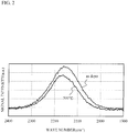
- FIG. 2 is a diagram that enlarges parts close to Si-H signals of a silicon nitride film having a refractive index of 2.35, and illustrates a signal immediately after the silicon nitride film is grown (as depo) and another signal after the silicon nitride film is annealed at 500 °C.
- the bonds of silicon and hydrogen decrease by annealing. This shows that the bonds of silicon and hydrogen are broken and hydrogen is removed from the silicon nitride film.
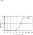
- FIG. 3 illustrates a result of investigation of the quantity of removed hydrogen when a silicon nitride film having a refractive index of 2.35 is annealed by using TDS (Thermal Desorption Spectroscopy).
- the horizontal axis denotes temperature
- the vertical axis denotes ion current of hydrogen, which is a quantity corresponding to the quantity of hydrogen removed from the silicon nitride film.
- removal of hydrogen initiates when the temperature of the silicon nitride film exceeds 350 °C (which is 50 °C higher than the temperature at which the silicon nitride film is grown).
- the temperature of the silicon nitride film is equal to or higher than 500 °C, hydrogen is removed drastically.
- the quantity of removed hydrogen is saturated when the temperature rises over 600 °C.
- the inventors supposed that the instable phenomenon such as power slump is caused by such a factor that electros in the GaN-based semiconductor layer are captured to non-bonded arms of Si resulting from removal of hydrogen.
- a factor of removal of hydrogen may be annealing after the source electrode and the drain electrode are formed.
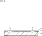
- FIG. 4 is a diagram for describing the principle of the present invention, and is a cross-sectional view that illustrates a fabrication step of FET.
- a source electrode 16 and a drain electrode 18 are formed on a GaN- or InP-based semiconductor layer 11.
- a silicon-rich silicon nitride film 12 and an insulation film 15 are formed on the semiconductor layer 11 between the source electrode 16 and the drain electrode 18. In this state, annealing is carried out.
- the silicon-rich silicon nitride film 12 is a film having a refractive index of 2.2 or higher, and is formed so as to be thin within a thickness enough to react impurity elements at an interface between the semiconductor layer 11 and the silicon nitride film 12 such as oxygen.
- the insulation film 15 is a silicon nitride film from which hydrogen is hard to be removed, and the above silicon nitride film has a low refractive index.
- the insulation film 15 is an insulation film in which charges such as electrons are hard to be captured. It is thus possible to restrain the charges in the semiconductor layer 11 such as electrons from being captured in the insulation film 15 and to suppress the instable phenomenon resulting from capturing the charges in the insulation film 15 such as power slump.
- Embodiment 1 is an example in which the insulation film is a silicon nitride film having a low refractive index.
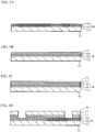
- FIG. 5A through FIG. 7B are diagrams that illustrate a method for fabricating a semiconductor device in accordance with embodiment 1.
- a GaN travel layer 52 on a substrate 10 made of SiC, Si or sapphire, formed are a GaN travel layer 52, an AlGaN electron supply layer 54, and a GaN cap layer 56 by MOCVD (Metal Organic CVD).
- MOCVD Metal Organic CVD
- a first silicon nitride film 12 that has a refractive index of 2.35 and a film thickness of 10 nm is formed on the GaN cap layer 56 at a growth temperature of about 300 °C by using PECVD.
- a second silicon nitride film 14 that has a refractive index of 2.0 and a film thickness of 10 nm is formed on the first silicon nitride film 12 at a growth temperature of about 300 °C.
- a photoresist 30 is formed on the second silicon nitride film 14, and the GaN cap layer 56 is exposed in areas in which the source electrode and the drain electrode are formed by an exposure method and an etching method.
- Ta and Al are evaporated in turn from the epitaxial layer 58 side, and the source electrode 16 and the drain electrode 18 are formed in the areas in which the GaN cap layer 56 is exposed.
- An evaporated material 17 of Ta and Al is also formed on the photoresist 30.
- the source electrode 16 and the drain electrode 18 are annealed at 565 °C in the state in which the first silicon nitride film 12 and the second silicon nitride film 14 are formed.
- the source electrode 16 and the drain electrode 18 are brought into ohmic-contact to the GaN cap layer 56.
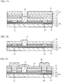
- a third silicon nitride film 20 that has a refractive index of 2.0 and a film thickness of 40 nm is formed on the source electrode 16, the drain electrode 18 and the second silicon nitride film 14 at a growth temperature of about 300 °C by PECVD.
- the third silicon nitride film 20 is a protection film for protecting the gaps between the source electrode 16 or the drain electrode 18 and the second silicon nitride film 14.
- a two-layer photoresist 36 composed of a lower layer 32 and an upper layer 34 is formed. From the epitaxial layer 58 side, Ni and Au are evaporated in turn. An evaporated material 23 is formed on the photoresist 36. Thus, the gate electrode 22 is formed on the GaN cap layer 56 between the source electrode 16 and the drain electrode 18.
- liftoff is performed.
- a silicon nitride film 40 having a film thickness of 400 nm is grown by PECVD. Then, a photoresist (not illustrated) is formed on the silicon nitride film 40, and the surfaces of the source electrode 16 and the drain electrode 18 are exposed.
- TiW is formed on the source electrode 16 and the drain electrode 18 by evaporation, and then, Au is formed thereon by plating. Finally, liftoff of the photoresist is performed. This results in interconnection layer 42 composed of TiW and Au. Now, the FET of embodiment 1 is completed.
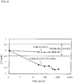
- FIG. 8 is a diagram that illustrates results of a test of energizing of FETs configured in accordance with a comparative example and embodiment 1.
- the comparative example is an FET in which only the first silicon nitride film 12 is grown.
- a method for fabricating the comparative example is as follows. In FIG. 5C , the first silicon nitride film 12 that has a refractive index of 2.35 and a film thickness of about 50 nm is grown, and the steps of FIGS. 6A through 7E are carried out without forming the second silicon nitride film 14 illustrated in FIG. 5D .
- the other fabrication steps are the same as those of FIGS. 5A through 7C .
- the gate lengths and the gate widths of the comparative example and embodiment 1 are 0.6 ⁇ m and 2.25 mm, respectively.
- the energizing condition has a channel temperature of 250 °C, a drain voltage of 50 V, and a drain current of 100 mA.
- the horizontal axis of FIG. 8 is the energizing time, and the vertical axis denotes variation ⁇ Psat in the saturated power before energizing is initiated. The saturated power is measured in such a manner that energizing is stopped to return the temperature to room temperature and the output power of RF is then measured.
- the saturated power is reduced due to high-temperature energizing, and the power slump is observed. In contrast, there is little variation in the saturated power even after high-temperature energizing.
- the power slump may be suppressed, as compared to the comparative example.
- FIG. 9 is a diagram that illustrates results of a high-temperature energizing test of sample FETs in which the refractive index of the second silicon nitride film 14 is within the range of 1.8 to 2.6.
- the method for the high-temperature energizing test is the same as illustrated in FIG. 8 .
- the sample FETs were prepared so that the refractive indexes of the second silicon nitride films 14 of the sample FETs are 1.8, 1.9, 2.0, 2.1, 2.15, 2.25, 2.35 and 2.6, and the other fabrications steps are the same as those illustrated in FIGs. 5A through 7B .
- the following may be considered as the reason why the power slump takes place when the second silicon nitride film 14 has a high refractive index.
- hydrogen in the first silicon nitride film 12 having a high refractive index and the second silicon nitride film 14 is removed by annealing (see FIG. 6B ) at 565 °C for obtaining ohmic contacts of the source electrode 16 and the drain electrode 18.
- annealing see FIG. 6B
- many arms of silicon that are not bonded are formed in the first silicon nitride film 12 and the second silicon nitride film 14.
- the charges in semiconductor of the FET are captured by the arms of silicon that are not bonded in the first silicon nitride film 12 and the second silicon nitride film 14. The above may cause the power slump.
- the following may be considered as the reason why the power slump is suppressed in the case where the second silicon nitride film 14 has a low refractive index.
- the refractive index of the second silicon nitride film 14 is low, hydrogen and nitrogen are bonded strongly, and hydrogen bonded to nitrogen is hard to be removed even at high temperature.
- hydrogen in the second silicon nitride film 14 is not removed even by annealing the source electrode 16 and the drain electrode 18. This makes it possible to prevent the charges from being captured in the second silicon nitride film 14 even by drain energizing at high temperature and to suppress the occurrence of power slump.
- the refractive index of the first silicon nitride film 12 should be 2.2 or higher in order to suppress the collapse phenomenon.
- the refractive index of the second silicon nitride film 14 is lower than that of the first silicon nitride film 12. Thus, it is possible to suppress the power slump as well as the collapse phenomenon.
- the refractive index of the first silicon nitride film 12 is 2.6 or higher, the silicon nitride film is amorphous silicon, and leakage current between the gate electrode 22 and the drain electrode 18 increases. It is thus preferable that the refractive index of the first silicon nitride film 12 is equal to or lower than 2.6.
- the refractive index of the first silicon nitride film 12 is preferably in the range of 2.2 to 2.5, and is more preferably in the range of 2.3 to 2.4.
- FIG. 10A is a diagram that illustrates a profile of an atomic ratio of Si, N, Ga and O with respect to the depth of a sample in which a silicon nitride film having a refractive index of 2.2 is formed on a GaN layer by PECVD prior to annealing.
- FIG. 10B is a diagram that illustrates a profile of an atomic ratio with respect to the depth of a sample similar to that in FIG. 10A after annealing at 565 °C.
- a position at which the depth is zero is the interface between GaN and SiN.
- a region in which the depth is positive is SiN, and another region in which the depth is negative is GaN.
- XPS X-ray Photoelectron Spectroscopy
- O (oxygen) in the GaN layer is taken to the silicon nitride film due to annealing.
- oxygen at the interface of the GaN layer to the silicon nitride film is decreased.
- oxygen is detected in the depth up to about 20 nm from the interface of the silicon nitride film. That is, a film thickness of about 20 nm of the silicon nitride film makes it possible to considerably take oxygen from the GaN layer to the silicon nitride film.
- FIGs. 11A and 11B illustrate profiles of atomic ratios with respect to the depth of samples in which a silicon nitride film having a refractive index of 2.6 is formed on a GaN layer by PEDVD prior to and after annealing at 565 °C, respectively.
- O oxygen
- FIGs. 11A and 11B O (oxygen) in the GaN layer is taken to the silicon nitride film due to annealing. After annealing, oxygen is detected in the depth up to about 10 nm from the interface of the silicon nitride film. That is, a film thickness of about 10 nm of the silicon nitride film makes it possible to considerably take oxygen from the GaN layer to the silicon nitride film.
- the film thickness of the first silicon nitride film 12 may be set equal to or more than 10 nm. Further, in order to restrain the charges in the semiconductor layer from being captured by the arms of silicon that are not bonded in the first silicon nitride film 12, it is preferable that the first silicon nitride is thin. From FIG. 11B , the effect of taking oxygen to the silicon nitride film is not enhanced even when the film thickness of the first silicon nitride film is 20 nm or more. That is, it is preferable that the film thickness of the first silicon nitride film is equal to or less than 20 nm. Thus, in the range of 2.2 to 2.6 of the refractive index of the first silicon nitride film 12, the film thickness of the first silicon nitride film 12 is preferably in the range of 10 nm to 20 nm.
- the tolerable range of variation of saturated power by high-temperature energizing is generally ⁇ 0.5 dB.
- the refractive index of the second silicon nitride film 14 is equal to or higher than 1.9 and is equal to or lower than 2.1.
- the film thickness of the second silicon nitride film 14 is preferably equal to or more than 10 nm in terms of preventing removal of hydrogen, and is preferably equal to or less than 100 nm in terms of producing the fine gate electrode.
- hydrogen in the silicon nitride film is removed by annealing at a temperature that is 50 °C or higher than the growth temperature of the silicon nitride film.
- the anneal temperature is 50 °C or higher than the growth temperature of the first silicon nitride film 12
- the power slump is likely to occur
- the second silicon nitride film 14 is preferably employed.
- the temperature of annealing for making ohmic contacts in FIG. 6B is 500 °C or higher, hydrogen in the silicon nitride film is likely to be removed.
- the anneal temperature is 550 °C or higher, hydrogen in the silicon nitride film is more likely to be removed.
- the use of the second silicon nitride film 14 is advantageous when the anneal temperature is 500 °C, preferably, when the anneal temperature is 550 °C.
- An exemplary condition for growing the first silicon nitride film 12 and the second silicon nitride film 14 may have a growth temperature of about 300 °C, an SiH 4 flow rate of 4 - 15 sccm, an NH 3 flow rate of 0 - 8 sccm, an N 2 flow rate of 20 - 700 sccm, an He flow rate of 0 - 800 sccm, and an RF power of 0.04 - 0.24 W/cm 2 .
- Embodiment 2 is an example in which the insulation film formed on the first silicon nitride film is other than the silicon nitride film.
- FIG. 12A through FIG. 12E are diagrams that illustrate a method for fabricating a semiconductor device in accordance with embodiment 2.
- the insulation film 15 is formed on the first silicon nitride film 12 after FIG. 5C of embodiment 1.
- the insulation film 15 is any of silicon oxide, aluminum oxide, tantalum oxide, strontium oxide, hafnium oxide, aluminum nitride, lanthanum oxide, yttrium oxide, and zirconium oxide.
- FIG. 12B as in the case of FIG. 6B of embodiment 1, the source electrode 16 and the drain electrode 18 are formed.
- a photoresist 38 having an opening in a gate electrode forming area is formed on the source electrode 16, the drain electrode 18 and the insulation film 15.
- the gate electrode 22 is evaporated.
- the evaporated material 23 is formed on the photoresist 38.
- liftoff is carried out.
- FIG. 12E as in the case of FIG. 7C of embodiment 1, the silicon nitride film 40 and the interconnection layer 42 are formed.
- the insulation film 15 is used instead of the second silicon nitride film 14 employed in embodiment 1.
- the insulation film 15 is hard to capture charges, as compared to the silicon nitride film. Thus, the power slump may be suppressed.
- the gate electrode 22 may be formed on the insulation film 15 so that a MIS (Metal Insulator Semiconductor) FET may be configured. That is, the step of forming the gate electrode 22 in FIG. 10 may be varied so as to form the gate electrode 22 on the insulation film 15. Particularly, when it is difficult to etch the insulation film 15, it is preferable that the gate electrode 22 is formed on the insulation film 15.
- the gate insulation film may include a film other than the insulation film 15.
- the FETs having the GaN-based semiconductor layers are described as an example.
- the semiconductor layer on which the first silicon nitride film 12 is formed may be on the AlGaN electron supply layer 54.
- the FET having the GaN-based semiconductor layer on the surface as described in Patent Document 1, it is preferable to reduce gallium oxide on the surface.
- the semiconductor layer on which the first silicon nitride film 12 is formed may be another GaN-based semiconductor layer.
- the GaN-based semiconductor may be AlN, InN, InGaN other than GaN and AlGaN.
- the FET having the InP-based semiconductor layer on the surface P in the InP-based semiconductor is likely to be removed, and the surface of the InP-based semiconductor is In-rich. In this case, In is bonded to oxygen in the atmosphere, and In oxide is formed. As in the case of embodiments 1 to 2, even in the case where a silicon-rich silicon nitride film is formed on the InP-based semiconductor, it is possible to remove impurities such as In oxide at the interface between the InP-based semiconductor and the first silicon nitride film 12. Thus, the FET having the InP-based semiconductor layer is capable of suppressing the collapse phenomenon and the power slump as in the case of the FET having the GaN-based semiconductor layer.
- the InP-based semiconductor may be InP, InGaP, InAlGaP, and so on.
Landscapes
- Junction Field-Effect Transistors (AREA)
- Formation Of Insulating Films (AREA)
- Thin Film Transistor (AREA)
- Insulated Gate Type Field-Effect Transistor (AREA)
Claims (7)
- Verfahren zur Herstellung eines Halbleiterbauelements, wobei das Verfahren Folgendes umfasst:Ausbilden eines ersten Siliziumnitridfilms (12) mit einem Brechungsindex von 2,2 oder höher auf einer Halbleiterschicht (11) aus einem Halbleiter auf GaN- oder InP-Basis;Ausbilden, auf dem ersten Siliziumnitridfilm (12),entweder eines zweiten Siliziumnitridfilms (14) mit einem Brechungsindex, der niedriger ist als der des ersten Siliziumnitridfilms (12),oder eines Isolierfilms (15), der aus einem von Siliziumoxid, Aluminiumoxid, Tantaloxid, Strontiumoxid, Hafniumoxid, Aluminiumnitrid, Lanthanoxid, Yttriumoxid und Zirkonoxid besteht;Ausbilden einer Source-Elektrode (16) und einer Drain-Elektrode (18) in Bereichen, in denen die Halbleiterschicht (11) frei liegt;Tempern der Source-Elektrode (16) und der Drain-Elektrode (18) in einem Zustand, in dem der erste Siliziumnitridfilm (12) und der zweite Siliziumnitridfilm (14) oder der erste Siliziumnitridfilm (12) und der Isolierfilm (15) gebildet werden; undAusbilden einer Gate-Elektrode (22) auf der Halbleiterschicht (11) zwischen der Source-Elektrode (16) und der Drain-Elektrode (18).
- Verfahren nach Anspruch 1, wobei der erste Siliziumnitridfilm (12) eine Filmdicke von 10-20 nm hat.
- Verfahren nach Anspruch 1 oder 2, wobei der erste Siliziumnitridfilm (12) einen Brechungsindex von 2,6 oder niedriger hat.
- Verfahren nach Anspruch 1, 2 oder 3, wobei der Schritt des Tempern bei einer Temperatur ausgeführt wird, die 50°C oder höher ist als eine Temperatur, bei der der erste Siliziumnitridfilm (12) gebildet wird.
- Verfahren nach einem der vorangehenden Ansprüche, wobei der zweite Siliziumnitridfilm (14) auf dem ersten Siliziumnitridfilm (12) gebildet wird und der zweite Siliziumnitridfilm (14) einen Brechungsindex hat, der mindestens 1,9 und maximal 2.1 beträgt.
- Verfahren nach einem der vorangehenden Ansprüche, wobei der zweite Siliziumnitridfilm (14) auf dem ersten Siliziumnitridfilm (12) gebildet wird und der zweite Siliziumnitridfilm (14) eine Filmdicke von 10-100 nm hat.
- Verfahren nach einem der Ansprüche 1-4, wobei der Isolierfilm (15) auf dem ersten Siliziumnitridfilm (12) gebildet wird und der Schritt des Ausbildens der Gate-Elektrode (22) einen Schritt des Ausbildens der Gate-Elektrode (22) auf dem Isolierfilm (15) enthält.
Applications Claiming Priority (2)
| Application Number | Priority Date | Filing Date | Title |
|---|---|---|---|
| JP2008041345A JP5345328B2 (ja) | 2008-02-22 | 2008-02-22 | 半導体装置の製造方法 |
| PCT/JP2009/052537 WO2009104554A1 (ja) | 2008-02-22 | 2009-02-16 | 半導体装置の製造方法 |
Publications (4)
| Publication Number | Publication Date |
|---|---|
| EP2246880A1 EP2246880A1 (de) | 2010-11-03 |
| EP2246880A4 EP2246880A4 (de) | 2013-09-25 |
| EP2246880B1 true EP2246880B1 (de) | 2016-12-21 |
| EP2246880B8 EP2246880B8 (de) | 2017-06-28 |
Family
ID=40985435
Family Applications (1)
| Application Number | Title | Priority Date | Filing Date |
|---|---|---|---|
| EP09712194.1A Active EP2246880B8 (de) | 2008-02-22 | 2009-02-16 | Verfahren zur herstellung eines halbleiterbauelements |
Country Status (4)
| Country | Link |
|---|---|
| US (1) | US8354312B2 (de) |
| EP (1) | EP2246880B8 (de) |
| JP (1) | JP5345328B2 (de) |
| WO (1) | WO2009104554A1 (de) |
Families Citing this family (23)
| Publication number | Priority date | Publication date | Assignee | Title |
|---|---|---|---|---|
| JP5685020B2 (ja) | 2010-07-23 | 2015-03-18 | 住友電気工業株式会社 | 半導体装置の製造方法 |
| JP5725749B2 (ja) * | 2010-07-28 | 2015-05-27 | 住友電工デバイス・イノベーション株式会社 | 半導体装置の製造方法 |
| JP2012033689A (ja) * | 2010-07-30 | 2012-02-16 | Sumitomo Electric Device Innovations Inc | 半導体装置の製造方法 |
| JP6035007B2 (ja) * | 2010-12-10 | 2016-11-30 | 富士通株式会社 | Mis型の窒化物半導体hemt及びその製造方法 |
| JP2012151261A (ja) * | 2011-01-19 | 2012-08-09 | Mitsubishi Heavy Ind Ltd | 半導体発光素子、半導体発光素子の保護膜及びその作製方法 |
| US9070758B2 (en) * | 2011-06-20 | 2015-06-30 | Imec | CMOS compatible method for manufacturing a HEMT device and the HEMT device thereof |
| JP5166576B2 (ja) * | 2011-07-07 | 2013-03-21 | シャープ株式会社 | GaN系半導体素子の製造方法 |
| JP6025242B2 (ja) | 2012-03-30 | 2016-11-16 | 住友電工デバイス・イノベーション株式会社 | 半導体装置の製造方法 |
| KR102099445B1 (ko) * | 2012-06-29 | 2020-04-09 | 가부시키가이샤 한도오따이 에네루기 켄큐쇼 | 반도체 장치 및 반도체 장치의 제작 방법 |
| JP2014072391A (ja) * | 2012-09-28 | 2014-04-21 | Fujitsu Ltd | 化合物半導体装置及びその製造方法 |
| JP6106908B2 (ja) * | 2012-12-21 | 2017-04-05 | 住友電工デバイス・イノベーション株式会社 | 半導体装置の製造方法 |
| JP6093190B2 (ja) * | 2013-01-18 | 2017-03-08 | 住友電気工業株式会社 | Mis構造トランジスタ、及びmis構造トランジスタを作製する方法 |
| JP6241915B2 (ja) * | 2013-07-31 | 2017-12-06 | 住友電工デバイス・イノベーション株式会社 | 半導体装置の製造方法 |
| KR102270823B1 (ko) * | 2013-10-22 | 2021-06-30 | 가부시키가이샤 한도오따이 에네루기 켄큐쇼 | 반도체 장치와 그 제작 방법 |
| JP2016054250A (ja) * | 2014-09-04 | 2016-04-14 | 豊田合成株式会社 | 半導体装置、製造方法、方法 |
| US9580304B2 (en) * | 2015-05-07 | 2017-02-28 | Texas Instruments Incorporated | Low-stress low-hydrogen LPCVD silicon nitride |
| JP6627441B2 (ja) * | 2015-11-11 | 2020-01-08 | 住友電気工業株式会社 | 半導体装置 |
| US9741557B1 (en) * | 2016-06-23 | 2017-08-22 | Texas Instruments Incorporated | Silicon nitride process for reduction of threshold shift |
| JP6649586B2 (ja) * | 2016-07-12 | 2020-02-19 | 富士通株式会社 | 化合物半導体装置及びその製造方法 |
| JP6650867B2 (ja) * | 2016-12-22 | 2020-02-19 | 三菱電機株式会社 | ヘテロ接合電界効果型トランジスタの製造方法 |
| JP7031282B2 (ja) * | 2017-12-20 | 2022-03-08 | 富士通株式会社 | 半導体装置及びその製造方法、高周波増幅器 |
| JP7327173B2 (ja) | 2020-01-10 | 2023-08-16 | 住友電気工業株式会社 | 半導体装置及び半導体装置の製造方法 |
| JP7740799B2 (ja) * | 2021-09-27 | 2025-09-17 | 住友電工デバイス・イノベーション株式会社 | 半導体装置及び半導体装置の製造方法 |
Family Cites Families (13)
| Publication number | Priority date | Publication date | Assignee | Title |
|---|---|---|---|---|
| US7012297B2 (en) * | 2001-08-30 | 2006-03-14 | Micron Technology, Inc. | Scalable flash/NV structures and devices with extended endurance |
| JP4385206B2 (ja) * | 2003-01-07 | 2009-12-16 | 日本電気株式会社 | 電界効果トランジスタ |
| JP4179539B2 (ja) * | 2003-01-15 | 2008-11-12 | 富士通株式会社 | 化合物半導体装置及びその製造方法 |
| JP2004273658A (ja) * | 2003-03-07 | 2004-09-30 | Nippon Telegr & Teleph Corp <Ntt> | ナイトライド系半導体素子の作製法 |
| JP2004288952A (ja) * | 2003-03-24 | 2004-10-14 | Fujitsu Ltd | 電界効果トランジスタ及びその製造方法 |
| JP2006279032A (ja) * | 2005-03-02 | 2006-10-12 | Matsushita Electric Ind Co Ltd | 半導体装置及びその製造方法 |
| JP4912604B2 (ja) | 2005-03-30 | 2012-04-11 | 住友電工デバイス・イノベーション株式会社 | 窒化物半導体hemtおよびその製造方法。 |
| JP4897948B2 (ja) * | 2005-09-02 | 2012-03-14 | 古河電気工業株式会社 | 半導体素子 |
| US7419892B2 (en) * | 2005-12-13 | 2008-09-02 | Cree, Inc. | Semiconductor devices including implanted regions and protective layers and methods of forming the same |
| US7709269B2 (en) * | 2006-01-17 | 2010-05-04 | Cree, Inc. | Methods of fabricating transistors including dielectrically-supported gate electrodes |
| JP5186776B2 (ja) * | 2007-02-22 | 2013-04-24 | 富士通株式会社 | 半導体装置及びその製造方法 |
| US7750370B2 (en) * | 2007-12-20 | 2010-07-06 | Northrop Grumman Space & Mission Systems Corp. | High electron mobility transistor having self-aligned miniature field mitigating plate on a protective dielectric layer |
| JP4719210B2 (ja) * | 2007-12-28 | 2011-07-06 | 富士通株式会社 | 半導体装置及びその製造方法 |
-
2008
- 2008-02-22 JP JP2008041345A patent/JP5345328B2/ja active Active
-
2009
- 2009-02-16 WO PCT/JP2009/052537 patent/WO2009104554A1/ja not_active Ceased
- 2009-02-16 EP EP09712194.1A patent/EP2246880B8/de active Active
-
2010
- 2010-08-20 US US12/860,454 patent/US8354312B2/en active Active
Non-Patent Citations (1)
| Title |
|---|
| None * |
Also Published As
| Publication number | Publication date |
|---|---|
| WO2009104554A1 (ja) | 2009-08-27 |
| JP5345328B2 (ja) | 2013-11-20 |
| EP2246880A4 (de) | 2013-09-25 |
| JP2009200306A (ja) | 2009-09-03 |
| EP2246880A1 (de) | 2010-11-03 |
| US20100317164A1 (en) | 2010-12-16 |
| EP2246880B8 (de) | 2017-06-28 |
| US8354312B2 (en) | 2013-01-15 |
Similar Documents
| Publication | Publication Date | Title |
|---|---|---|
| EP2246880B1 (de) | Verfahren zur herstellung eines halbleiterbauelements | |
| CN107946358B (zh) | 一种与Si-CMOS工艺兼容的AlGaN/GaN异质结HEMT器件及其制作方法 | |
| JP5203220B2 (ja) | 支持されたゲート電極を備えるトランジスタの作製方法およびそれに関連するデバイス | |
| US7906799B2 (en) | Nitride-based transistors with a protective layer and a low-damage recess | |
| US9024324B2 (en) | GaN dual field plate device with single field plate metal | |
| US9633920B2 (en) | Low damage passivation layer for III-V based devices | |
| EP2575178B1 (de) | Verbundhalbleiterbauelement und Herstellungsverfahren dafür | |
| US8653558B2 (en) | Semiconductor device and method of making | |
| CN103177960B (zh) | 对硅衬底上的iii族氮化物的衬底击穿电压的改进 | |
| JP2009283915A (ja) | 浅いイオン注入された領域を含む半導体デバイスとその形成方法 | |
| TW201405823A (zh) | 使用再成長結構之三族氮化物電晶體 | |
| CN207925477U (zh) | 一种与Si-CMOS工艺兼容的AlGaN/GaN异质结HEMT器件 | |
| WO2023019436A1 (en) | Semiconductor device and method for manufacturing the same | |
| WO2022205469A1 (en) | Iii nitride semiconductor wafers | |
| EP2117039B1 (de) | Halbleitervorrichtungen mit flachimplantierten Bereichen und Verfahren zur Bildung davon | |
| CN224054687U (zh) | 高电子迁移率晶体管设备和电子设备 | |
| WO2024092543A1 (en) | Nitride-based semiconductor device and method for manufacturing the same | |
| WO2024040465A1 (en) | Nitride-based semiconductor device and method for manufacturing the same | |
| US20260040601A1 (en) | Group iii-n device including a hydrogen-blocking layer | |
| Koehler et al. | Engineering pecvd sin passivation layers to enable algan/gan hemts with low leakage, low current collapse and high breakdown voltage International Conference on Compound Semiconductor Manufacturing Technology | |
| Pang | Development of high-performance gan-based power transistors | |
| US20070148879A1 (en) | III-V compound semiconductor heterostructure MOSFET with a high workfunction metal gate electrode and process of making the same |
Legal Events
| Date | Code | Title | Description |
|---|---|---|---|
| PUAI | Public reference made under article 153(3) epc to a published international application that has entered the european phase |
Free format text: ORIGINAL CODE: 0009012 |
|
| 17P | Request for examination filed |
Effective date: 20100915 |
|
| AK | Designated contracting states |
Kind code of ref document: A1 Designated state(s): AT BE BG CH CY CZ DE DK EE ES FI FR GB GR HR HU IE IS IT LI LT LU LV MC MK MT NL NO PL PT RO SE SI SK TR |
|
| AX | Request for extension of the european patent |
Extension state: AL BA RS |
|
| RAP1 | Party data changed (applicant data changed or rights of an application transferred) |
Owner name: SUMITOMO ELECTRIC DEVICE INNOVATIONS, INC. |
|
| DAX | Request for extension of the european patent (deleted) | ||
| A4 | Supplementary search report drawn up and despatched |
Effective date: 20130826 |
|
| RIC1 | Information provided on ipc code assigned before grant |
Ipc: H01L 29/778 20060101ALI20130820BHEP Ipc: H01L 21/318 20060101ALI20130820BHEP Ipc: H01L 29/812 20060101ALI20130820BHEP Ipc: H01L 21/338 20060101AFI20130820BHEP Ipc: H01L 29/786 20060101ALI20130820BHEP |
|
| GRAP | Despatch of communication of intention to grant a patent |
Free format text: ORIGINAL CODE: EPIDOSNIGR1 |
|
| INTG | Intention to grant announced |
Effective date: 20160602 |
|
| GRAS | Grant fee paid |
Free format text: ORIGINAL CODE: EPIDOSNIGR3 |
|
| GRAJ | Information related to disapproval of communication of intention to grant by the applicant or resumption of examination proceedings by the epo deleted |
Free format text: ORIGINAL CODE: EPIDOSDIGR1 |
|
| GRAL | Information related to payment of fee for publishing/printing deleted |
Free format text: ORIGINAL CODE: EPIDOSDIGR3 |
|
| GRAR | Information related to intention to grant a patent recorded |
Free format text: ORIGINAL CODE: EPIDOSNIGR71 |
|
| INTC | Intention to grant announced (deleted) | ||
| RIN1 | Information on inventor provided before grant (corrected) |
Inventor name: KOMATANI, TSUTOMU |
|
| GRAA | (expected) grant |
Free format text: ORIGINAL CODE: 0009210 |
|
| AK | Designated contracting states |
Kind code of ref document: B1 Designated state(s): AT BE BG CH CY CZ DE DK EE ES FI FR GB GR HR HU IE IS IT LI LT LU LV MC MK MT NL NO PL PT RO SE SI SK TR |
|
| INTG | Intention to grant announced |
Effective date: 20161116 |
|
| REG | Reference to a national code |
Ref country code: GB Ref legal event code: FG4D |
|
| REG | Reference to a national code |
Ref country code: CH Ref legal event code: EP |
|
| REG | Reference to a national code |
Ref country code: IE Ref legal event code: FG4D |
|
| REG | Reference to a national code |
Ref country code: AT Ref legal event code: REF Ref document number: 856154 Country of ref document: AT Kind code of ref document: T Effective date: 20170115 |
|
| REG | Reference to a national code |
Ref country code: DE Ref legal event code: R096 Ref document number: 602009043198 Country of ref document: DE |
|
| REG | Reference to a national code |
Ref country code: FR Ref legal event code: PLFP Year of fee payment: 9 |
|
| PG25 | Lapsed in a contracting state [announced via postgrant information from national office to epo] |
Ref country code: LV Free format text: LAPSE BECAUSE OF FAILURE TO SUBMIT A TRANSLATION OF THE DESCRIPTION OR TO PAY THE FEE WITHIN THE PRESCRIBED TIME-LIMIT Effective date: 20161221 |
|
| REG | Reference to a national code |
Ref country code: DE Ref legal event code: R083 Ref document number: 602009043198 Country of ref document: DE |
|
| RIN2 | Information on inventor provided after grant (corrected) |
Inventor name: KOMATANI, TSUTOMU |
|
| REG | Reference to a national code |
Ref country code: LT Ref legal event code: MG4D |
|
| REG | Reference to a national code |
Ref country code: NL Ref legal event code: MP Effective date: 20161221 |
|
| PG25 | Lapsed in a contracting state [announced via postgrant information from national office to epo] |
Ref country code: NO Free format text: LAPSE BECAUSE OF FAILURE TO SUBMIT A TRANSLATION OF THE DESCRIPTION OR TO PAY THE FEE WITHIN THE PRESCRIBED TIME-LIMIT Effective date: 20170321 Ref country code: LT Free format text: LAPSE BECAUSE OF FAILURE TO SUBMIT A TRANSLATION OF THE DESCRIPTION OR TO PAY THE FEE WITHIN THE PRESCRIBED TIME-LIMIT Effective date: 20161221 Ref country code: GR Free format text: LAPSE BECAUSE OF FAILURE TO SUBMIT A TRANSLATION OF THE DESCRIPTION OR TO PAY THE FEE WITHIN THE PRESCRIBED TIME-LIMIT Effective date: 20170322 Ref country code: SE Free format text: LAPSE BECAUSE OF FAILURE TO SUBMIT A TRANSLATION OF THE DESCRIPTION OR TO PAY THE FEE WITHIN THE PRESCRIBED TIME-LIMIT Effective date: 20161221 |
|
| REG | Reference to a national code |
Ref country code: AT Ref legal event code: MK05 Ref document number: 856154 Country of ref document: AT Kind code of ref document: T Effective date: 20161221 |
|
| PG25 | Lapsed in a contracting state [announced via postgrant information from national office to epo] |
Ref country code: HR Free format text: LAPSE BECAUSE OF FAILURE TO SUBMIT A TRANSLATION OF THE DESCRIPTION OR TO PAY THE FEE WITHIN THE PRESCRIBED TIME-LIMIT Effective date: 20161221 Ref country code: BE Free format text: LAPSE BECAUSE OF NON-PAYMENT OF DUE FEES Effective date: 20170228 Ref country code: FI Free format text: LAPSE BECAUSE OF FAILURE TO SUBMIT A TRANSLATION OF THE DESCRIPTION OR TO PAY THE FEE WITHIN THE PRESCRIBED TIME-LIMIT Effective date: 20161221 |
|
| PG25 | Lapsed in a contracting state [announced via postgrant information from national office to epo] |
Ref country code: NL Free format text: LAPSE BECAUSE OF FAILURE TO SUBMIT A TRANSLATION OF THE DESCRIPTION OR TO PAY THE FEE WITHIN THE PRESCRIBED TIME-LIMIT Effective date: 20161221 |
|
| PG25 | Lapsed in a contracting state [announced via postgrant information from national office to epo] |
Ref country code: EE Free format text: LAPSE BECAUSE OF FAILURE TO SUBMIT A TRANSLATION OF THE DESCRIPTION OR TO PAY THE FEE WITHIN THE PRESCRIBED TIME-LIMIT Effective date: 20161221 Ref country code: RO Free format text: LAPSE BECAUSE OF FAILURE TO SUBMIT A TRANSLATION OF THE DESCRIPTION OR TO PAY THE FEE WITHIN THE PRESCRIBED TIME-LIMIT Effective date: 20161221 Ref country code: CZ Free format text: LAPSE BECAUSE OF FAILURE TO SUBMIT A TRANSLATION OF THE DESCRIPTION OR TO PAY THE FEE WITHIN THE PRESCRIBED TIME-LIMIT Effective date: 20161221 Ref country code: SK Free format text: LAPSE BECAUSE OF FAILURE TO SUBMIT A TRANSLATION OF THE DESCRIPTION OR TO PAY THE FEE WITHIN THE PRESCRIBED TIME-LIMIT Effective date: 20161221 Ref country code: IS Free format text: LAPSE BECAUSE OF FAILURE TO SUBMIT A TRANSLATION OF THE DESCRIPTION OR TO PAY THE FEE WITHIN THE PRESCRIBED TIME-LIMIT Effective date: 20170421 |
|
| PG25 | Lapsed in a contracting state [announced via postgrant information from national office to epo] |
Ref country code: ES Free format text: LAPSE BECAUSE OF FAILURE TO SUBMIT A TRANSLATION OF THE DESCRIPTION OR TO PAY THE FEE WITHIN THE PRESCRIBED TIME-LIMIT Effective date: 20161221 Ref country code: BE Free format text: LAPSE BECAUSE OF FAILURE TO SUBMIT A TRANSLATION OF THE DESCRIPTION OR TO PAY THE FEE WITHIN THE PRESCRIBED TIME-LIMIT Effective date: 20161221 Ref country code: BG Free format text: LAPSE BECAUSE OF FAILURE TO SUBMIT A TRANSLATION OF THE DESCRIPTION OR TO PAY THE FEE WITHIN THE PRESCRIBED TIME-LIMIT Effective date: 20170321 Ref country code: PL Free format text: LAPSE BECAUSE OF FAILURE TO SUBMIT A TRANSLATION OF THE DESCRIPTION OR TO PAY THE FEE WITHIN THE PRESCRIBED TIME-LIMIT Effective date: 20161221 Ref country code: AT Free format text: LAPSE BECAUSE OF FAILURE TO SUBMIT A TRANSLATION OF THE DESCRIPTION OR TO PAY THE FEE WITHIN THE PRESCRIBED TIME-LIMIT Effective date: 20161221 Ref country code: IT Free format text: LAPSE BECAUSE OF FAILURE TO SUBMIT A TRANSLATION OF THE DESCRIPTION OR TO PAY THE FEE WITHIN THE PRESCRIBED TIME-LIMIT Effective date: 20161221 Ref country code: PT Free format text: LAPSE BECAUSE OF FAILURE TO SUBMIT A TRANSLATION OF THE DESCRIPTION OR TO PAY THE FEE WITHIN THE PRESCRIBED TIME-LIMIT Effective date: 20170421 |
|
| REG | Reference to a national code |
Ref country code: DE Ref legal event code: R097 Ref document number: 602009043198 Country of ref document: DE |
|
| PG25 | Lapsed in a contracting state [announced via postgrant information from national office to epo] |
Ref country code: MC Free format text: LAPSE BECAUSE OF FAILURE TO SUBMIT A TRANSLATION OF THE DESCRIPTION OR TO PAY THE FEE WITHIN THE PRESCRIBED TIME-LIMIT Effective date: 20161221 |
|
| REG | Reference to a national code |
Ref country code: CH Ref legal event code: PL |
|
| PLBE | No opposition filed within time limit |
Free format text: ORIGINAL CODE: 0009261 |
|
| STAA | Information on the status of an ep patent application or granted ep patent |
Free format text: STATUS: NO OPPOSITION FILED WITHIN TIME LIMIT |
|
| PG25 | Lapsed in a contracting state [announced via postgrant information from national office to epo] |
Ref country code: LI Free format text: LAPSE BECAUSE OF NON-PAYMENT OF DUE FEES Effective date: 20170228 Ref country code: CH Free format text: LAPSE BECAUSE OF NON-PAYMENT OF DUE FEES Effective date: 20170228 |
|
| 26N | No opposition filed |
Effective date: 20170922 |
|
| REG | Reference to a national code |
Ref country code: IE Ref legal event code: MM4A |
|
| PG25 | Lapsed in a contracting state [announced via postgrant information from national office to epo] |
Ref country code: DK Free format text: LAPSE BECAUSE OF FAILURE TO SUBMIT A TRANSLATION OF THE DESCRIPTION OR TO PAY THE FEE WITHIN THE PRESCRIBED TIME-LIMIT Effective date: 20161221 |
|
| PG25 | Lapsed in a contracting state [announced via postgrant information from national office to epo] |
Ref country code: LU Free format text: LAPSE BECAUSE OF NON-PAYMENT OF DUE FEES Effective date: 20170216 |
|
| REG | Reference to a national code |
Ref country code: FR Ref legal event code: PLFP Year of fee payment: 10 |
|
| PG25 | Lapsed in a contracting state [announced via postgrant information from national office to epo] |
Ref country code: SI Free format text: LAPSE BECAUSE OF FAILURE TO SUBMIT A TRANSLATION OF THE DESCRIPTION OR TO PAY THE FEE WITHIN THE PRESCRIBED TIME-LIMIT Effective date: 20161221 Ref country code: IE Free format text: LAPSE BECAUSE OF NON-PAYMENT OF DUE FEES Effective date: 20170216 |
|
| PG25 | Lapsed in a contracting state [announced via postgrant information from national office to epo] |
Ref country code: MT Free format text: LAPSE BECAUSE OF NON-PAYMENT OF DUE FEES Effective date: 20170216 |
|
| PG25 | Lapsed in a contracting state [announced via postgrant information from national office to epo] |
Ref country code: HU Free format text: LAPSE BECAUSE OF FAILURE TO SUBMIT A TRANSLATION OF THE DESCRIPTION OR TO PAY THE FEE WITHIN THE PRESCRIBED TIME-LIMIT; INVALID AB INITIO Effective date: 20090216 |
|
| PG25 | Lapsed in a contracting state [announced via postgrant information from national office to epo] |
Ref country code: CY Free format text: LAPSE BECAUSE OF NON-PAYMENT OF DUE FEES Effective date: 20161221 |
|
| PG25 | Lapsed in a contracting state [announced via postgrant information from national office to epo] |
Ref country code: MK Free format text: LAPSE BECAUSE OF FAILURE TO SUBMIT A TRANSLATION OF THE DESCRIPTION OR TO PAY THE FEE WITHIN THE PRESCRIBED TIME-LIMIT Effective date: 20161221 |
|
| PG25 | Lapsed in a contracting state [announced via postgrant information from national office to epo] |
Ref country code: TR Free format text: LAPSE BECAUSE OF FAILURE TO SUBMIT A TRANSLATION OF THE DESCRIPTION OR TO PAY THE FEE WITHIN THE PRESCRIBED TIME-LIMIT Effective date: 20161221 |
|
| REG | Reference to a national code |
Ref country code: DE Ref legal event code: R082 Ref document number: 602009043198 Country of ref document: DE Representative=s name: HL KEMPNER PATENTANWAELTE, SOLICITORS (ENGLAND, DE Ref country code: DE Ref legal event code: R082 Ref document number: 602009043198 Country of ref document: DE Representative=s name: HL KEMPNER PATENTANWALT, RECHTSANWALT, SOLICIT, DE Ref country code: DE Ref legal event code: R082 Ref document number: 602009043198 Country of ref document: DE Representative=s name: HL KEMPNER PARTG MBB, DE |
|
| P01 | Opt-out of the competence of the unified patent court (upc) registered |
Effective date: 20230515 |
|
| REG | Reference to a national code |
Ref country code: DE Ref legal event code: R079 Ref document number: 602009043198 Country of ref document: DE Free format text: PREVIOUS MAIN CLASS: H01L0021338000 Ipc: H10D0030870000 |
|
| PGFP | Annual fee paid to national office [announced via postgrant information from national office to epo] |
Ref country code: FR Payment date: 20251231 Year of fee payment: 18 |
|
| PGFP | Annual fee paid to national office [announced via postgrant information from national office to epo] |
Ref country code: GB Payment date: 20260106 Year of fee payment: 18 |
|
| PGFP | Annual fee paid to national office [announced via postgrant information from national office to epo] |
Ref country code: DE Payment date: 20251230 Year of fee payment: 18 |