EP2246882A1 - Procédé de transfert d'une couche à partir d'un substrat donneur sur un substrat lié - Google Patents
Procédé de transfert d'une couche à partir d'un substrat donneur sur un substrat lié Download PDFInfo
- Publication number
- EP2246882A1 EP2246882A1 EP09290314A EP09290314A EP2246882A1 EP 2246882 A1 EP2246882 A1 EP 2246882A1 EP 09290314 A EP09290314 A EP 09290314A EP 09290314 A EP09290314 A EP 09290314A EP 2246882 A1 EP2246882 A1 EP 2246882A1
- Authority
- EP
- European Patent Office
- Prior art keywords
- substrate
- donor
- donor substrate
- layer
- handle
- Prior art date
- Legal status (The legal status is an assumption and is not a legal conclusion. Google has not performed a legal analysis and makes no representation as to the accuracy of the status listed.)
- Granted
Links
Images



Classifications
-
- H—ELECTRICITY
- H10—SEMICONDUCTOR DEVICES; ELECTRIC SOLID-STATE DEVICES NOT OTHERWISE PROVIDED FOR
- H10P—GENERIC PROCESSES OR APPARATUS FOR THE MANUFACTURE OR TREATMENT OF DEVICES COVERED BY CLASS H10
- H10P52/00—Grinding, lapping or polishing of wafers, substrates or parts of devices
- H10P52/40—Chemomechanical polishing [CMP]
- H10P52/402—Chemomechanical polishing [CMP] of semiconductor materials
-
- H—ELECTRICITY
- H10—SEMICONDUCTOR DEVICES; ELECTRIC SOLID-STATE DEVICES NOT OTHERWISE PROVIDED FOR
- H10P—GENERIC PROCESSES OR APPARATUS FOR THE MANUFACTURE OR TREATMENT OF DEVICES COVERED BY CLASS H10
- H10P90/00—Preparation of wafers not covered by a single main group of this subclass, e.g. wafer reinforcement
- H10P90/12—Preparing bulk and homogeneous wafers
- H10P90/16—Preparing bulk and homogeneous wafers by reclaiming or re-processing
-
- H—ELECTRICITY
- H10—SEMICONDUCTOR DEVICES; ELECTRIC SOLID-STATE DEVICES NOT OTHERWISE PROVIDED FOR
- H10P—GENERIC PROCESSES OR APPARATUS FOR THE MANUFACTURE OR TREATMENT OF DEVICES COVERED BY CLASS H10
- H10P90/00—Preparation of wafers not covered by a single main group of this subclass, e.g. wafer reinforcement
- H10P90/19—Preparing inhomogeneous wafers
- H10P90/1904—Preparing vertically inhomogeneous wafers
- H10P90/1906—Preparing SOI wafers
- H10P90/1914—Preparing SOI wafers using bonding
- H10P90/1916—Preparing SOI wafers using bonding with separation or delamination along an ion implanted layer, e.g. Smart-cut
-
- H—ELECTRICITY
- H10—SEMICONDUCTOR DEVICES; ELECTRIC SOLID-STATE DEVICES NOT OTHERWISE PROVIDED FOR
- H10W—GENERIC PACKAGES, INTERCONNECTIONS, CONNECTORS OR OTHER CONSTRUCTIONAL DETAILS OF DEVICES COVERED BY CLASS H10
- H10W10/00—Isolation regions in semiconductor bodies between components of integrated devices
- H10W10/10—Isolation regions comprising dielectric materials
- H10W10/181—Semiconductor-on-insulator [SOI] isolation regions, e.g. buried oxide regions of SOI wafers
Definitions
- the invention relates to a method for transferring a layer from a donor substrate onto a handle substrate and for reclaiming the surface of the donor substrate for reuse.
- the so-called Smart Cut TM process illustrated in Figure 1 provides high quality silicon on insulator (SOI) substrates.
- SOI silicon on insulator
- two substrates called a handle substrate 101 and a donor substrate 103, usually Silicon wafers, undergo a certain number of process steps to transfer a layer with a given thickness of the donor substrate 103 onto the handle substrate 101.
- the donor substrate 103 is typically oxidized 105 to later on form the buried oxide layer (BOX) of the SOI structure, and an ion implantation step, during which ions like hydrogen or rare gas ions (He, Ar, ..) are implanted into the donor substrate 103, is applied to form a predetermined splitting area 107 defining the to-be-transferred layer.
- an ion implantation step during which ions like hydrogen or rare gas ions (He, Ar, ..) are implanted into the donor substrate 103, is applied to form a predetermined splitting area 107 defining the to-be-transferred layer.
- the source substrate 103 is attached to the handle substrate 101, in particular via bonding taking advantage of Van der Waal's forces, to obtain a source-handle compound 109.
- a detachment of a semiconductor layer 111 together with the buried oxide layer 113 occurs at the predetermined splitting area 107 so that the two layers are transferred onto the handle substrate 101 to obtain the desired silicon on insulator structure 115 ( Figure 1c ).
- the thickness of the layer 111 is determined by the energy of the implanted ions.
- the remaining part 117 of the donor substrate 101 can be recycled and again used in the Smart Cut TM type process as a new donor or handle substrate.
- the Smart Cut TM type SOI fabrication process has a significant economic advantage due to this recycling process. Indeed, the process provides an optimized use of the raw material for instance silicon wafers.
- the negative 117 ( Figure 1c ) has a characteristic topography representing protruding residues 119a and 119b in an edge region, as illustrated in Figure 1 , which corresponds to a region where no layer transfer occurred due to the chamfered shape of the edge of the initial wafers 103 and/or 101.
- the surface of the negative 117 between the protruding residues 119a and 119b has a first inner region 121 at which detachment occurred to provide the transferred layer 111 on the handle substrate 109 and which has a rather rough surface typically close to 60 - 70 ⁇ RMS as measured by atomic force microscopy (AFM), which is to be compared to 1 - 3 ⁇ for standard Silicon wafer.
- AFM atomic force microscopy
- the edge of the remainder 117 with the protruding residues 119a and 119b actually has a chamfered shape and furthermore comprises a step-like structure 123 seen from the internal region 121 comprising the remaining part of the buried oxide layer 125 and the non-transferred silicon 127 over the remaining part of the ion implanted predetermined splitting area 129.
- the edge 131 and the backside 133 of the negative 117 are, by the way, also covered by the oxide.
- the step 123 of the negative 117 typically has a thickness of about 100-10000 ⁇ of silicon, mostly between 1000 to 3000 ⁇ , and 100 to 10000 ⁇ of silicon oxide and has a width w in the lateral direction of the order of 0.5 - 3 mm.
- the surface roughness of the inner region 121 needs to be reduced and the protruding residual topography 119a & 119b needs to be removed.
- the removal needs to be complete as any remaining protruding material can create particle contamination when during a thermal treatment an exfoliation in the chamfered region occurs due the presence of the remaining ion implanted region 129. Methods to do so are, for example, known from EP 1 156 531 A1 and US 7,402,520 B2 .
- the reclaiming process of negative 117 starts with a de-oxidation step to remove the oxide layer 125 on top of the protruding residual topography on the edge of the remainder 117 as well as on the side 131 and on its backside 133.
- the de-oxidation can, for example, be carried out using a HF bath, wherein the acid consumes the oxide layer 125, 131 and 133.
- a first polishing step of the edge region of substrate 1 is carried out to at least partially remove the protruding silicon part 127 on the edge.
- a double-sided polishing (DSP) step is carried out to improve the surface roughness in the interior region 121 but also to further remove the step 123 in the direction of the protruding residual topography 119a and 119b, but also to remove residues remaining form the ion implantation.
- DSP double-sided polishing
- CMP chemical mechanical polishing step
- the DSP process step has the major disadvantage that, during polishing, up to 10 ⁇ m (5 ⁇ m on each side of the substrate) of material are removed to get rid of the protruding residual topography 119a and 119b.
- the method comprises the steps of a) providing a donor substrate, in particular a semiconductor substrate, and a handle substrate each with chamfered edge regions, b) forming a predetermined splitting area at a depth h inside the donor substrate, c) attaching, in particular by bonding, the donor and the handle substrate to obtain a donor-handle compound, wherein no attaching occurs between the two substrates in the chamfered edge regions of the donor and handle substrates, then d) etching the chamfered region such that at least a layer of about the thickness h is removed from the donor substrate in the region where no attaching occurred, then e) detaching a remainder of the donor substrate from the donor handle substrate, wherein detachment occurs at the predetermined splitting area and f) reusing the remainder of the donor substrate, in particular after the surface treatment step.
- a layer with a thickness of more than h is removed.
- the remainder of the donor substrate will no longer present a protruding portion 119a, 119b as illustrated in Figure 1 , as the chamfered area where no attachment occurs between the two attached substrates is removed prior to the detachment.
- the edge removal step and the double-sided polishing step which were mandatory in the prior art to get rid of the protruding portion.
- the reclaiming of the remainder of the donor substrate can be carried out in a much simpler way not needing expensive additional tools to carry out the edge polishing and the double-sided polishing process steps.
- the initial geometry of the donor substrates can be kept even if one donor substrate is used several times in a process as described above.
- the quality of the obtained substrates is also improved as the risk of creation of particles during a raise in temperature leading to a partial removal of the chamfered region, can be reduced.
- the method can use a donor substrate comprising a dielectric layer and, in this case, can furthermore comprise a step g) carried out between steps c) and d) which consists in removing the dielectric from the donor substrate at least in the chamfered region but not in the attached region.
- a dielectric used to form a semiconductor on insulator substrate with the mentioned process it is still possible to achieve the advantages of the method as, not only the chamfered region of the donor substrate itself but also of its dielectric layer, is removed prior to detaching.
- step g) is simply moved from after detachment to prior to detachment.
- the handle substrate can comprise a dielectric layer.
- the dielectric layer is provided by the handle substrate to form a semiconductor on insulator substrate.
- This variant has the advantage that one only has to remove the material of the substrate in step d) to achieve the advantages of the invention, as no additional dielectric layer is provided on the donor substrate. Thus, in this variant, less process steps are necessary compared to the variant which provides the dielectric via the donor substrate.
- the dielectric layer can be an oxide, in particular a silicon oxide.
- This oxide layer can be provided either by a thermal process or by deposition.
- steps e) and/or g) can be a wet or dry etching step. This is a more economic material removal step than the edge polishing and double-sided polished step as used in the prior art.
- steps e) and g) can be performed using a non-selective and/or isotropic etching solution.
- a non-selective and/or isotropic etching solution both the dielectric layer and the underlying part of the donor substrate, for instance a semiconductor material, can be removed in one step.
- an isotropic etching solution the process is furthermore simplified as varying etching rates, depending on the crystallographic directions which are different in the chamfered region compared to the rest of the substrate, do not have to be taken into account. This simplifies the control of the process.
- the dielectric material removal step independent of whether the dielectric layer is removed from the donor and/or the handle substrate (in case a dielectric is also present on the handle substrate), does not have an impact on the quality of the buried dielectric layer as this one is sandwiched between donor and handle substrate.
- a layer with a thickness of about 100 ⁇ - 10,000 ⁇ , in particular 1000 - 3000 ⁇ can be removed in the non-attached region of the donor substrate.
- the material removal in the process according the invention can be less so that one donor substrate can be reused more often, for instance, more than 10 times, compared to the prior art process. This is also made possible by the fact that the reclaimed donor substrate remains within the semi-standard concerning the substrate dimensions.
- steps d) and/or g) can be carried out at a temperature of less than 500°C, preferably at less than 350°C.
- steps d) and/or g) can be carried out at low temperature so that no detachment can occur in the non-attached regions which could lead to unwanted particle contamination of the final product.
- the surface treatment step can, at most, comprise a polishing step, in particular a CMP polishing and a cleaning step before and/or after the polishing step.
- a greatly simplified reclaiming process can be carried out.
- the polishing step is used to get the desired surface quality of the reclaimed remainder of the donor substrate, typically a mirror polished quality, and the cleaning steps, as known in the art, make the reclaimed donor substrate ready for reuse.
- the invention instead of a three-level reclaiming process: i) edge polishing, ii) double-sided polishing, iii) mirror polishing plus the various cleaning steps, the invention provides the possibility to carry out the reclaiming process with only one simple mirror polishing step.
- the term "about the thickness h" used in claim 1 relates to thickness that are such that the remainder can be planarised using only a CMP process. This means that a layer is removed in step d) of claim 1 that has a thickness of at least h minus about 50nm. This would lead to a protruding region in the remainder of the donor substrate with a height of about 50nm which can be dealt with by a simple CMP polishing step.
- a layer of less than 3 ⁇ m, preferably less than 1 ⁇ m, can be removed from the surface where detachment occurred.
- this limited material removal brings the advantage that one donor substrate can be reused more often, in particular, more than 10 times, in the layer transfer process.
- th;e handle substrate 101 can be any suitable handle substrate, in particular a silicon wafer, but also a glass or quartz type substrate.
- the donor substrate 103 can be a semiconductor substrate, in particular one out of a silicon, a silicon carbide, a silicon germanium, a gallium nitride or a germanium substrate and the isolating dielectric layer 105 can be one out of silicon dioxide, silicon nitride, silicon oxynitride or Al 2 O 3 , etc.
- a handle substrate 101 being a silicon wafer
- a donor substrate 103 being a silicon wafer
- the dielectric layer 105 being a silicon dioxide.
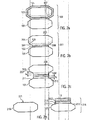
- Figure 2b illustrates the source-handle compound 201 obtained after an etching step during which the dielectric layer 105 has been from the back side 203, the side 205 but also the chamfered regions 207 and 209 of the donor substrate.
- a dielectric layer 105' remains sandwiched between the donor substrate 103 and the handle substrate 101 and forms the future buried oxide layer.
- the material removal is achieved with an etching step.
- the etching can be a dry or a wet etching suitable to remove the dielectric oxide layer which typically has a thickness of up to 1000 nm, but typically has a thickness of 10 - 200 nm.
- an additional etching step is carried out to remove the silicon present in the chamfered legion 207' and 209'.
- the etching step can again be a wet or dry etching and is preferably an isotropic etching for instance using a wet etch with HF/HNO 3 or a dry etch using a plasma.
- the dielectric etching and the semiconductor etching are carried out using the same process.
- the etching is carried out such that material is removed from the chamfered region 207' and 209' at least of the donor substrate 103 and such that the removed layer has a thickness h 1 corresponding to the depth h of the predetermined splitting area 107.
- the material removal not only occurs in the chamfered region but also on the side and on the back side of the donor substrate 103 and also in the chamfered region 211 and 213 of the handle substrate 101.
- the next step consists in a detachment step, the result of which is illustrated in Figure 2d and which is carried out in the same way as described in the introduction, thus either using mechanical and/or thermal energy.
- a semiconductor on insulator here silicon on insulator substrate 215, as illustrated on the right hand side of Figure 2d .
- This structure 215 comprises the handle substrate 101, the transferred oxide layer 105' and the transferred silicon layer 111 from the donor substrate 103. Due to the etching process, the substrate 215 furthermore comprises a step-like shoulder 217 in the chamfered edge regions 211 and 213 of the handle substrate 101 which makes the geometry of semiconductor on insulator substrate 215 slightly different compared to the one illustrated in Figure 1c .
- the effect of the inventive method is even more visible on the remainder 219 of the donor substrate 103 illustrated on the left hand side of Figure 2d .
- the remainder of the donor substrate 219, according to the invention no longer has a protruding portion in its edge region which is in complete contrast to the structure 117 according to the prior art illustrated in the left hand side of Figure 1c in the prior art.
- the surface part 221 where detachment occurred has a rather rough surface, with roughness values close to 60 - 70 ⁇ like in the prior art.
- the surface roughness can be improved by a simple CMP polishing process during which less than 3 ⁇ m, preferably less than 1 ⁇ m, or even only about 50nm, of material is removed from the surface to obtain the desired surface quality for reuse of the reclaimed remainder 219.
- the chemical/mechanical polishing step can be accompanied by standard cleaning processes as in the prior art.
- the method according to the first embodiment has the advantage that, after detachment, no protruding portions are present in the edge regions, which is in complete contrast with the prior art, see reference numerals 119a, 119b in Figure 1 .
- the reclaiming process to recondition the remainder of the donor substrate 219 such that it can be reduced is greatly simplified. No edge polishing and no double-sided polishing are necessary anymore and a simple CMP process is sufficient to obtain the desired surface quality properties, eventually accompanied by one or two cleaning steps.
- the recycling process is not only cheaper to carry, as less equipment is necessary for the process, but also one donor substrate can be reused more often.
- the inventive process can be carried out with a greatly reduced material removal of the order of less than 3 ⁇ m, typically 0.5 - 1 ⁇ m. It is even possible to carry out the reclaiming process by only removing about 50nm from the surface 221. Thus, one donor substrate 103 can be recycled more often than in the prior art, namely about at least 10 times. Due to the fact that no DSP is necessary, also the geometry of the initial substrate can be kept. Besides, another important advantage is, that the creation of particles during step e), i.e.
- thermal treatment leading to the detachment or any subsequent thermal treatment step can be prevented or at least reduced as, in the chamfered region, the remaining ion implanted part is removed so that it cannot explode away during a subsequent thermal treatment and thus the creation of undesired particles can be reduced or even prevented.
- Figures 3a - 3e illustrate a second embodiment of the inventive method for transferring a layer of a donor substrate 103 onto a handle substrate 101.
- Figure 3a again illustrates the source-handle compound 109, the description there of is not repeated again but incorporated herewith by reference to the description of Figure 2a .
- Figure 3b illustrating the resulting structure 201 after the dielectric material removal step.
- the difference between the first embodiment and the second embodiment is that, during the etching of the chamfered region 207" and 209" of the donor substrate 103, the material removal goes beyond the depth of the predetermined splitting area 107, 129, as illustrated in Figure 3c , by reference numeral h2. Again, the predetermined splitting area 107 is still present within the donor substrate 103. As a consequence of the longer etching process, also the material removal in the chamfered region 211' and 213' of the handle substrate 101 is of the order of h2.
- the additional material removal has the advantage that it is ensured that all implanted areas 129 present in the chamfered region 207 and 209 are removed.
- the semiconductor on insulator substrate 301 is obtained which essentially corresponds to the one 215 illustrated on the right hand side of Figure 2d .
- the step-like region 303 at the transition between the chamfered region 211' and 213' and the buried oxide layer 105' is higher (h2) than in the semiconductor on insulator structure 215 of Figure 2d .
- the remainder of the donor substrate 305 in this embodiment also has a step-like smoulder 307 with a step height h2.
- the surface 309 at which detachment occurred still carries defects due to the ion implantation and thus needs to be polished.
- the polishing step is carried out such that the step-like structure 307 is removed so that a ready to reuse donor substrate 311, as illustrated in Figure 3e , is obtained.
- This substrate 311 is again flat, except for the chamfered region, which is like in the original substrate 103,' except for a reduced thickness.
- the process could be carried out without an intervening dielectric layer, which is called a direct silicon bonding process.
- the first and second embodiments could be carried out without the step of removing the dielectric 105, as illustrated in Figures 2b and 3b .
- Figures 4a - 4d illustrate a third embodiment of the invention.
- This embodiment is slightly different compared to the first and second embodiments as, here, the dielectric layer is provided on the handle substrate side and the donor substrate is a bare semiconductor wafer, for instance a silicon wafer.
- the materials that can be used in this embodiment correspond to the ones of the first and second embodiment.
- FIG. 4a illustrates the donor substrate 401 with a predetermined splitting area 403 and the right side the handle substrate 405, which in this case also comprises a dielectric layer, for instance silicon oxide, 407.
- a dielectric layer for instance silicon oxide
- Figure 4b illustrates the source handle compound 409 achieved by bonding the donor and the handle substrate 401 and 405. Like in the first and second embodiment on the surface side where bonding occurred a non attached region 411 and 413 can be observed which is due to the chamfered edge region of both substrates.
- a etching step is carried out to remove a layer of thickness h 1 corresponding to the depth h of the predetermined splitting are 403 is removed in the non attached edge regions 411' and 413'.
- the ion implanted region 129 in the edge region of the donor substrate 401 is removed by this step.
- the donor substrate 401 is not covered by the dielectric layer, which is in contrast to the first and second embodiment, no oxide removal step is necessary in this embodiment.
- a SOI substrate 415 is obtained comprising a transferred layer 417 and a buried oxide layer 419 still part of the original dielectric layer 407 covering the handle substrate 405.
- a deoxidation step could be carried out to remove the layer 407 except for the buried part 415 to obtain a SOI substrate as illustrated in Figures 2d or 3d .
- the remainder 421 of the original donor substrate 401 has the same structure than the one illustrated in Figure 2d .
- a simple CMP polishing process is sufficient to remove the defects on the surface 423 where detachment occurred.
- the material removal step illustrated in Figure 4c could also be carried out such that a thickness h 2 is removed is larger than the depth h of the predetermined splitting area 403, just like in the second embodiment.
- the first till third embodiments can also be carried out without the presence of a buried oxide layer 105'.
- a buried oxide layer 105' In the so called direct silicon bonding technology two Si wafers typically one with a 100 and the other one with a 110 surface are bonded together. In this case the process described are carried out in the same way without however the step of removing the oxide by etching. It should furthermore be mentioned that by CMP a remaining protruding portion of about 50nm, which could be,present in the edge region in case the material removal did not go up until h or beyond, can still be removed.
- Example one according to the invention a Silicon on insulator substrate with a buried thermal oxide of thickness 145 nm and a transferred layer of thickness 250nm is achieved using an etching process of the source handle substrate as illustrated in Figure 2b .
- the remainder of the donor substrate is recycled using a CMP process removing a layer with thickness of 0.5 ⁇ m.
- a two step selective etching is carried out: first the HF removes the oxide but does not etch Si, and the second bath using HF/HNO3 eventually buffered using CH 3 COOH acid etches the silicon.
- the recycling of the remainder is carried out by an EP and CMP step,
- the HF/H 2 O 2 bath is not selective and both layers the oxide and the silicon can be etched in one step.
- Edge polishing is performed to get rid of any potential residue of the implanted layer on the edge since material removal did not go up until h or beyond (h 1 ⁇ h -50nm), but the remaining 50 nm can also be removed with a CMP step and no EP polishing.
- a first plasma based on CF 4 or CHF 3 etches the oxide and then a second plasma on the basis of SF 6 etches the silicon.
- one of the two substrates, preferably the donor substrate has one of its main surfaces, called the back surface, on a substrate holder which prevents etching of the back side.
- the reclaiming of the remainder of the donor substrate comprises an additional deoxidation step to remove the oxide from the back side plus the CMP step polishing the front surface and removing about 1 ⁇ m of Silicon.
Landscapes
- Element Separation (AREA)
- Mechanical Treatment Of Semiconductor (AREA)
- Container, Conveyance, Adherence, Positioning, Of Wafer (AREA)
Priority Applications (8)
| Application Number | Priority Date | Filing Date | Title |
|---|---|---|---|
| EP09290314.5A EP2246882B1 (fr) | 2009-04-29 | 2009-04-29 | Procédé de transfert d'une couche à partir d'un substrat donneur sur un substrat de manipulation |
| JP2010040332A JP2010263187A (ja) | 2009-04-29 | 2010-02-25 | ドナー基板からハンドル基板へ層を転写するための方法 |
| US12/712,938 US8476148B2 (en) | 2009-04-29 | 2010-02-25 | Method for transferring a layer from a donor substrate onto a handle substrate |
| SG201001743-2A SG166047A1 (en) | 2009-04-29 | 2010-03-12 | Method for transferring a layer from a donor substrate onto a handle substrate |
| KR1020100022964A KR101650166B1 (ko) | 2009-04-29 | 2010-03-15 | 도너 기판으로부터 핸들 기판 상으로의 층 전달 방법 |
| TW099107511A TWI487014B (zh) | 2009-04-29 | 2010-03-15 | 自施體基板轉移一層至處理基板之方法 |
| CN201010199577.1A CN101877308B (zh) | 2009-04-29 | 2010-03-23 | 从施主衬底到处理衬底的层转移方法 |
| US13/933,779 US8728913B2 (en) | 2009-04-29 | 2013-07-02 | Method for transferring a layer from a donor substrate onto a handle substrate |
Applications Claiming Priority (1)
| Application Number | Priority Date | Filing Date | Title |
|---|---|---|---|
| EP09290314.5A EP2246882B1 (fr) | 2009-04-29 | 2009-04-29 | Procédé de transfert d'une couche à partir d'un substrat donneur sur un substrat de manipulation |
Publications (2)
| Publication Number | Publication Date |
|---|---|
| EP2246882A1 true EP2246882A1 (fr) | 2010-11-03 |
| EP2246882B1 EP2246882B1 (fr) | 2015-03-04 |
Family
ID=41116012
Family Applications (1)
| Application Number | Title | Priority Date | Filing Date |
|---|---|---|---|
| EP09290314.5A Active EP2246882B1 (fr) | 2009-04-29 | 2009-04-29 | Procédé de transfert d'une couche à partir d'un substrat donneur sur un substrat de manipulation |
Country Status (7)
| Country | Link |
|---|---|
| US (2) | US8476148B2 (fr) |
| EP (1) | EP2246882B1 (fr) |
| JP (1) | JP2010263187A (fr) |
| KR (1) | KR101650166B1 (fr) |
| CN (1) | CN101877308B (fr) |
| SG (1) | SG166047A1 (fr) |
| TW (1) | TWI487014B (fr) |
Cited By (2)
| Publication number | Priority date | Publication date | Assignee | Title |
|---|---|---|---|---|
| EP2770524A4 (fr) * | 2011-10-17 | 2015-07-22 | Shinetsu Handotai Kk | Procédé permettant de récupérer une tranche décollée |
| FR3076393A1 (fr) * | 2017-12-28 | 2019-07-05 | Commissariat A L'energie Atomique Et Aux Energies Alternatives | Procede de transfert d'une couche utile |
Families Citing this family (7)
| Publication number | Priority date | Publication date | Assignee | Title |
|---|---|---|---|---|
| EP2246882B1 (fr) | 2009-04-29 | 2015-03-04 | Soitec | Procédé de transfert d'une couche à partir d'un substrat donneur sur un substrat de manipulation |
| FR3007576B1 (fr) * | 2013-06-19 | 2015-07-10 | Soitec Silicon On Insulator | Procede de transfert d'une couche de circuits. |
| FR3036223B1 (fr) * | 2015-05-11 | 2018-05-25 | Commissariat A L'energie Atomique Et Aux Energies Alternatives | Procede de collage direct de substrats avec amincissement des bords d'au moins un des deux substrats |
| DE102015210384A1 (de) | 2015-06-05 | 2016-12-08 | Soitec | Verfahren zur mechanischen Trennung für eine Doppelschichtübertragung |
| US20180033609A1 (en) * | 2016-07-28 | 2018-02-01 | QMAT, Inc. | Removal of non-cleaved/non-transferred material from donor substrate |
| TWI741911B (zh) * | 2020-12-16 | 2021-10-01 | 環球晶圓股份有限公司 | 磊晶層去除方法 |
| CN117393422B (zh) * | 2023-12-11 | 2024-03-01 | 青禾晶元(天津)半导体材料有限公司 | 一种制造碳化硅复合衬底的方法 |
Citations (6)
| Publication number | Priority date | Publication date | Assignee | Title |
|---|---|---|---|---|
| EP1026728A2 (fr) * | 1999-02-02 | 2000-08-09 | Canon Kabushiki Kaisha | Substrat et méthode de fabrication associée |
| EP1156531A1 (fr) | 1999-11-29 | 2001-11-21 | Shin-Etsu Handotai Company Limited | Procede de recyclage d'une plaquette separee et plaquette separee recyclee |
| FR2852445A1 (fr) * | 2003-03-14 | 2004-09-17 | Soitec Silicon On Insulator | Procede de realisation de substrats ou composants sur substrats avec transfert de couche utile, pour la microelectronique, l'optoelectronique ou l'optique |
| FR2860842A1 (fr) * | 2003-10-14 | 2005-04-15 | Tracit Technologies | Procede de preparation et d'assemblage de substrats |
| WO2007017763A2 (fr) * | 2005-07-08 | 2007-02-15 | S.O.I. Tec Silicon On Insulator Technologies | Procede servant a produire une couche |
| US7402520B2 (en) | 2004-11-26 | 2008-07-22 | Applied Materials, Inc. | Edge removal of silicon-on-insulator transfer wafer |
Family Cites Families (10)
| Publication number | Priority date | Publication date | Assignee | Title |
|---|---|---|---|---|
| JPH11288858A (ja) * | 1998-01-30 | 1999-10-19 | Canon Inc | Soi基板の再生方法及び再生基板 |
| JP3932369B2 (ja) * | 1998-04-09 | 2007-06-20 | 信越半導体株式会社 | 剥離ウエーハを再利用する方法および再利用に供されるシリコンウエーハ |
| KR100359483B1 (ko) * | 2000-10-24 | 2002-10-31 | 고려용접봉 주식회사 | 가스 쉴드 아아크 용접용 플럭스 코어드 와이어 |
| FR2892228B1 (fr) * | 2005-10-18 | 2008-01-25 | Soitec Silicon On Insulator | Procede de recyclage d'une plaquette donneuse epitaxiee |
| JP4415588B2 (ja) * | 2003-08-28 | 2010-02-17 | 株式会社Sumco | 剥離ウェーハの再生処理方法 |
| WO2006037783A1 (fr) * | 2004-10-04 | 2006-04-13 | S.O.I.Tec Silicon On Insulator Technologies | Procédé de transfert d'une couche mince comprenant une perturbation controlée d'une structure cristalline |
| CN2923902Y (zh) * | 2006-07-27 | 2007-07-18 | 白宝鲲 | 点支式幕墙的吊装系统 |
| FR2907966B1 (fr) * | 2006-10-27 | 2009-01-30 | Soitec Silicon On Insulator | Procede de fabrication d'un substrat. |
| FR2917232B1 (fr) * | 2007-06-06 | 2009-10-09 | Soitec Silicon On Insulator | Procede de fabrication d'une structure pour epitaxie sans zone d'exclusion. |
| EP2246882B1 (fr) | 2009-04-29 | 2015-03-04 | Soitec | Procédé de transfert d'une couche à partir d'un substrat donneur sur un substrat de manipulation |
-
2009
- 2009-04-29 EP EP09290314.5A patent/EP2246882B1/fr active Active
-
2010
- 2010-02-25 JP JP2010040332A patent/JP2010263187A/ja active Pending
- 2010-02-25 US US12/712,938 patent/US8476148B2/en active Active
- 2010-03-12 SG SG201001743-2A patent/SG166047A1/en unknown
- 2010-03-15 KR KR1020100022964A patent/KR101650166B1/ko active Active
- 2010-03-15 TW TW099107511A patent/TWI487014B/zh active
- 2010-03-23 CN CN201010199577.1A patent/CN101877308B/zh active Active
-
2013
- 2013-07-02 US US13/933,779 patent/US8728913B2/en active Active
Patent Citations (6)
| Publication number | Priority date | Publication date | Assignee | Title |
|---|---|---|---|---|
| EP1026728A2 (fr) * | 1999-02-02 | 2000-08-09 | Canon Kabushiki Kaisha | Substrat et méthode de fabrication associée |
| EP1156531A1 (fr) | 1999-11-29 | 2001-11-21 | Shin-Etsu Handotai Company Limited | Procede de recyclage d'une plaquette separee et plaquette separee recyclee |
| FR2852445A1 (fr) * | 2003-03-14 | 2004-09-17 | Soitec Silicon On Insulator | Procede de realisation de substrats ou composants sur substrats avec transfert de couche utile, pour la microelectronique, l'optoelectronique ou l'optique |
| FR2860842A1 (fr) * | 2003-10-14 | 2005-04-15 | Tracit Technologies | Procede de preparation et d'assemblage de substrats |
| US7402520B2 (en) | 2004-11-26 | 2008-07-22 | Applied Materials, Inc. | Edge removal of silicon-on-insulator transfer wafer |
| WO2007017763A2 (fr) * | 2005-07-08 | 2007-02-15 | S.O.I. Tec Silicon On Insulator Technologies | Procede servant a produire une couche |
Cited By (3)
| Publication number | Priority date | Publication date | Assignee | Title |
|---|---|---|---|---|
| EP2770524A4 (fr) * | 2011-10-17 | 2015-07-22 | Shinetsu Handotai Kk | Procédé permettant de récupérer une tranche décollée |
| US9496130B2 (en) | 2011-10-17 | 2016-11-15 | Shin-Etsu Handotai Co., Ltd. | Reclaiming processing method for delaminated wafer |
| FR3076393A1 (fr) * | 2017-12-28 | 2019-07-05 | Commissariat A L'energie Atomique Et Aux Energies Alternatives | Procede de transfert d'une couche utile |
Also Published As
| Publication number | Publication date |
|---|---|
| US20130295696A1 (en) | 2013-11-07 |
| SG166047A1 (en) | 2010-11-29 |
| TWI487014B (zh) | 2015-06-01 |
| CN101877308B (zh) | 2016-03-09 |
| US20100279487A1 (en) | 2010-11-04 |
| TW201113939A (en) | 2011-04-16 |
| KR20100118932A (ko) | 2010-11-08 |
| EP2246882B1 (fr) | 2015-03-04 |
| CN101877308A (zh) | 2010-11-03 |
| KR101650166B1 (ko) | 2016-08-23 |
| US8476148B2 (en) | 2013-07-02 |
| US8728913B2 (en) | 2014-05-20 |
| JP2010263187A (ja) | 2010-11-18 |
Similar Documents
| Publication | Publication Date | Title |
|---|---|---|
| US8728913B2 (en) | Method for transferring a layer from a donor substrate onto a handle substrate | |
| US8617962B2 (en) | Method for finishing a substrate of the semiconductor-on-insulator type | |
| US8481409B2 (en) | Manufacturing process for a stacked structure comprising a thin layer bonding to a target substrate | |
| EP1189266B1 (fr) | Procede d'obtention de tranches de silicium ou de soi et tranches ainsi obtenues | |
| US6613676B1 (en) | Process of reclamation of SOI substrate and reproduced substrate | |
| KR101526245B1 (ko) | 임시 접합을 채용하는 반도체 구조를 제조하기 위한 방법 | |
| EP1894234A2 (fr) | Procede pour rigidite de substrat et dispositif resultant pour traitements a transfert de couche | |
| KR101536334B1 (ko) | 기판의 표면을 재생하는 방법 | |
| EP2246878B1 (fr) | Procédé de préparation de substrat SOI dont la face arrière est traitée par jet de sable | |
| US20220319910A1 (en) | Process for hydrophilically bonding substrates | |
| KR101752901B1 (ko) | 반도체 기판의 재생 방법, 재생 반도체 기판의 제작 방법, 및 soi 기판의 제작 방법 | |
| US20240145294A1 (en) | Method for manufacturing a silicon-carbide-based semiconductor structure and intermediate composite structure | |
| EP2048706B1 (fr) | Procédé de transfert avec traitement d'une surface à lier | |
| US20240170284A1 (en) | Method for producing a silicon carbide-based semiconductor structure and intermediate composite structure | |
| WO2008004591A1 (fr) | Procédé de production d'une tranche liée | |
| JPH11288858A (ja) | Soi基板の再生方法及び再生基板 | |
| EP1548822A1 (fr) | Procede de fabrication de plaquette silicium sur isolant | |
| US11424156B2 (en) | Removable structure and removal method using the structure | |
| TWI920243B (zh) | 用於製作碳化矽基半導體結構及中間複合結構之方法 |
Legal Events
| Date | Code | Title | Description |
|---|---|---|---|
| PUAI | Public reference made under article 153(3) epc to a published international application that has entered the european phase |
Free format text: ORIGINAL CODE: 0009012 |
|
| AK | Designated contracting states |
Kind code of ref document: A1 Designated state(s): AT BE BG CH CY CZ DE DK EE ES FI FR GB GR HR HU IE IS IT LI LT LU LV MC MK MT NL NO PL PT RO SE SI SK TR |
|
| AX | Request for extension of the european patent |
Extension state: AL BA RS |
|
| 17P | Request for examination filed |
Effective date: 20101216 |
|
| 17Q | First examination report despatched |
Effective date: 20110204 |
|
| R17C | First examination report despatched (corrected) |
Effective date: 20110517 |
|
| RAP1 | Party data changed (applicant data changed or rights of an application transferred) |
Owner name: SOITEC |
|
| REG | Reference to a national code |
Ref country code: DE Ref legal event code: R079 Ref document number: 602009029751 Country of ref document: DE Free format text: PREVIOUS MAIN CLASS: H01L0021762000 Ipc: H01L0021020000 |
|
| GRAP | Despatch of communication of intention to grant a patent |
Free format text: ORIGINAL CODE: EPIDOSNIGR1 |
|
| RIC1 | Information provided on ipc code assigned before grant |
Ipc: H01L 21/02 20060101AFI20140825BHEP Ipc: H01L 21/306 20060101ALI20140825BHEP |
|
| INTG | Intention to grant announced |
Effective date: 20140918 |
|
| GRAS | Grant fee paid |
Free format text: ORIGINAL CODE: EPIDOSNIGR3 |
|
| GRAA | (expected) grant |
Free format text: ORIGINAL CODE: 0009210 |
|
| AK | Designated contracting states |
Kind code of ref document: B1 Designated state(s): AT BE BG CH CY CZ DE DK EE ES FI FR GB GR HR HU IE IS IT LI LT LU LV MC MK MT NL NO PL PT RO SE SI SK TR |
|
| REG | Reference to a national code |
Ref country code: GB Ref legal event code: FG4D |
|
| REG | Reference to a national code |
Ref country code: CH Ref legal event code: EP |
|
| REG | Reference to a national code |
Ref country code: IE Ref legal event code: FG4D |
|
| REG | Reference to a national code |
Ref country code: NL Ref legal event code: T3 |
|
| REG | Reference to a national code |
Ref country code: AT Ref legal event code: REF Ref document number: 714510 Country of ref document: AT Kind code of ref document: T Effective date: 20150415 |
|
| REG | Reference to a national code |
Ref country code: DE Ref legal event code: R096 Ref document number: 602009029751 Country of ref document: DE Effective date: 20150416 |
|
| REG | Reference to a national code |
Ref country code: AT Ref legal event code: MK05 Ref document number: 714510 Country of ref document: AT Kind code of ref document: T Effective date: 20150304 |
|
| PG25 | Lapsed in a contracting state [announced via postgrant information from national office to epo] |
Ref country code: ES Free format text: LAPSE BECAUSE OF FAILURE TO SUBMIT A TRANSLATION OF THE DESCRIPTION OR TO PAY THE FEE WITHIN THE PRESCRIBED TIME-LIMIT Effective date: 20150304 Ref country code: NO Free format text: LAPSE BECAUSE OF FAILURE TO SUBMIT A TRANSLATION OF THE DESCRIPTION OR TO PAY THE FEE WITHIN THE PRESCRIBED TIME-LIMIT Effective date: 20150604 Ref country code: FI Free format text: LAPSE BECAUSE OF FAILURE TO SUBMIT A TRANSLATION OF THE DESCRIPTION OR TO PAY THE FEE WITHIN THE PRESCRIBED TIME-LIMIT Effective date: 20150304 Ref country code: LT Free format text: LAPSE BECAUSE OF FAILURE TO SUBMIT A TRANSLATION OF THE DESCRIPTION OR TO PAY THE FEE WITHIN THE PRESCRIBED TIME-LIMIT Effective date: 20150304 Ref country code: HR Free format text: LAPSE BECAUSE OF FAILURE TO SUBMIT A TRANSLATION OF THE DESCRIPTION OR TO PAY THE FEE WITHIN THE PRESCRIBED TIME-LIMIT Effective date: 20150304 Ref country code: SE Free format text: LAPSE BECAUSE OF FAILURE TO SUBMIT A TRANSLATION OF THE DESCRIPTION OR TO PAY THE FEE WITHIN THE PRESCRIBED TIME-LIMIT Effective date: 20150304 |
|
| REG | Reference to a national code |
Ref country code: LT Ref legal event code: MG4D |
|
| PG25 | Lapsed in a contracting state [announced via postgrant information from national office to epo] |
Ref country code: LV Free format text: LAPSE BECAUSE OF FAILURE TO SUBMIT A TRANSLATION OF THE DESCRIPTION OR TO PAY THE FEE WITHIN THE PRESCRIBED TIME-LIMIT Effective date: 20150304 Ref country code: AT Free format text: LAPSE BECAUSE OF FAILURE TO SUBMIT A TRANSLATION OF THE DESCRIPTION OR TO PAY THE FEE WITHIN THE PRESCRIBED TIME-LIMIT Effective date: 20150304 Ref country code: GR Free format text: LAPSE BECAUSE OF FAILURE TO SUBMIT A TRANSLATION OF THE DESCRIPTION OR TO PAY THE FEE WITHIN THE PRESCRIBED TIME-LIMIT Effective date: 20150605 |
|
| PG25 | Lapsed in a contracting state [announced via postgrant information from national office to epo] |
Ref country code: CZ Free format text: LAPSE BECAUSE OF FAILURE TO SUBMIT A TRANSLATION OF THE DESCRIPTION OR TO PAY THE FEE WITHIN THE PRESCRIBED TIME-LIMIT Effective date: 20150304 Ref country code: PT Free format text: LAPSE BECAUSE OF FAILURE TO SUBMIT A TRANSLATION OF THE DESCRIPTION OR TO PAY THE FEE WITHIN THE PRESCRIBED TIME-LIMIT Effective date: 20150706 Ref country code: SK Free format text: LAPSE BECAUSE OF FAILURE TO SUBMIT A TRANSLATION OF THE DESCRIPTION OR TO PAY THE FEE WITHIN THE PRESCRIBED TIME-LIMIT Effective date: 20150304 Ref country code: RO Free format text: LAPSE BECAUSE OF FAILURE TO SUBMIT A TRANSLATION OF THE DESCRIPTION OR TO PAY THE FEE WITHIN THE PRESCRIBED TIME-LIMIT Effective date: 20150304 Ref country code: EE Free format text: LAPSE BECAUSE OF FAILURE TO SUBMIT A TRANSLATION OF THE DESCRIPTION OR TO PAY THE FEE WITHIN THE PRESCRIBED TIME-LIMIT Effective date: 20150304 |
|
| PG25 | Lapsed in a contracting state [announced via postgrant information from national office to epo] |
Ref country code: IS Free format text: LAPSE BECAUSE OF FAILURE TO SUBMIT A TRANSLATION OF THE DESCRIPTION OR TO PAY THE FEE WITHIN THE PRESCRIBED TIME-LIMIT Effective date: 20150704 Ref country code: PL Free format text: LAPSE BECAUSE OF FAILURE TO SUBMIT A TRANSLATION OF THE DESCRIPTION OR TO PAY THE FEE WITHIN THE PRESCRIBED TIME-LIMIT Effective date: 20150304 Ref country code: MC Free format text: LAPSE BECAUSE OF FAILURE TO SUBMIT A TRANSLATION OF THE DESCRIPTION OR TO PAY THE FEE WITHIN THE PRESCRIBED TIME-LIMIT Effective date: 20150304 |
|
| REG | Reference to a national code |
Ref country code: CH Ref legal event code: PL |
|
| REG | Reference to a national code |
Ref country code: DE Ref legal event code: R097 Ref document number: 602009029751 Country of ref document: DE |
|
| PLBE | No opposition filed within time limit |
Free format text: ORIGINAL CODE: 0009261 |
|
| STAA | Information on the status of an ep patent application or granted ep patent |
Free format text: STATUS: NO OPPOSITION FILED WITHIN TIME LIMIT |
|
| REG | Reference to a national code |
Ref country code: IE Ref legal event code: MM4A |
|
| PG25 | Lapsed in a contracting state [announced via postgrant information from national office to epo] |
Ref country code: DK Free format text: LAPSE BECAUSE OF FAILURE TO SUBMIT A TRANSLATION OF THE DESCRIPTION OR TO PAY THE FEE WITHIN THE PRESCRIBED TIME-LIMIT Effective date: 20150304 Ref country code: LI Free format text: LAPSE BECAUSE OF NON-PAYMENT OF DUE FEES Effective date: 20150430 Ref country code: CH Free format text: LAPSE BECAUSE OF NON-PAYMENT OF DUE FEES Effective date: 20150430 Ref country code: IT Free format text: LAPSE BECAUSE OF NON-PAYMENT OF DUE FEES Effective date: 20150429 |
|
| REG | Reference to a national code |
Ref country code: NL Ref legal event code: MM Effective date: 20150501 |
|
| 26N | No opposition filed |
Effective date: 20151207 |
|
| PG25 | Lapsed in a contracting state [announced via postgrant information from national office to epo] |
Ref country code: SI Free format text: LAPSE BECAUSE OF FAILURE TO SUBMIT A TRANSLATION OF THE DESCRIPTION OR TO PAY THE FEE WITHIN THE PRESCRIBED TIME-LIMIT Effective date: 20150304 |
|
| REG | Reference to a national code |
Ref country code: FR Ref legal event code: PLFP Year of fee payment: 8 |
|
| PG25 | Lapsed in a contracting state [announced via postgrant information from national office to epo] |
Ref country code: IE Free format text: LAPSE BECAUSE OF NON-PAYMENT OF DUE FEES Effective date: 20150429 Ref country code: NL Free format text: LAPSE BECAUSE OF NON-PAYMENT OF DUE FEES Effective date: 20150501 |
|
| PG25 | Lapsed in a contracting state [announced via postgrant information from national office to epo] |
Ref country code: BE Free format text: LAPSE BECAUSE OF FAILURE TO SUBMIT A TRANSLATION OF THE DESCRIPTION OR TO PAY THE FEE WITHIN THE PRESCRIBED TIME-LIMIT Effective date: 20150304 |
|
| PG25 | Lapsed in a contracting state [announced via postgrant information from national office to epo] |
Ref country code: MT Free format text: LAPSE BECAUSE OF FAILURE TO SUBMIT A TRANSLATION OF THE DESCRIPTION OR TO PAY THE FEE WITHIN THE PRESCRIBED TIME-LIMIT Effective date: 20150304 |
|
| REG | Reference to a national code |
Ref country code: FR Ref legal event code: PLFP Year of fee payment: 9 |
|
| PG25 | Lapsed in a contracting state [announced via postgrant information from national office to epo] |
Ref country code: BG Free format text: LAPSE BECAUSE OF FAILURE TO SUBMIT A TRANSLATION OF THE DESCRIPTION OR TO PAY THE FEE WITHIN THE PRESCRIBED TIME-LIMIT Effective date: 20150304 Ref country code: HU Free format text: LAPSE BECAUSE OF FAILURE TO SUBMIT A TRANSLATION OF THE DESCRIPTION OR TO PAY THE FEE WITHIN THE PRESCRIBED TIME-LIMIT; INVALID AB INITIO Effective date: 20090429 |
|
| PG25 | Lapsed in a contracting state [announced via postgrant information from national office to epo] |
Ref country code: CY Free format text: LAPSE BECAUSE OF FAILURE TO SUBMIT A TRANSLATION OF THE DESCRIPTION OR TO PAY THE FEE WITHIN THE PRESCRIBED TIME-LIMIT Effective date: 20150304 |
|
| PG25 | Lapsed in a contracting state [announced via postgrant information from national office to epo] |
Ref country code: TR Free format text: LAPSE BECAUSE OF FAILURE TO SUBMIT A TRANSLATION OF THE DESCRIPTION OR TO PAY THE FEE WITHIN THE PRESCRIBED TIME-LIMIT Effective date: 20150304 |
|
| PG25 | Lapsed in a contracting state [announced via postgrant information from national office to epo] |
Ref country code: LU Free format text: LAPSE BECAUSE OF NON-PAYMENT OF DUE FEES Effective date: 20150429 |
|
| REG | Reference to a national code |
Ref country code: FR Ref legal event code: PLFP Year of fee payment: 10 |
|
| PG25 | Lapsed in a contracting state [announced via postgrant information from national office to epo] |
Ref country code: MK Free format text: LAPSE BECAUSE OF FAILURE TO SUBMIT A TRANSLATION OF THE DESCRIPTION OR TO PAY THE FEE WITHIN THE PRESCRIBED TIME-LIMIT Effective date: 20150304 |
|
| PGFP | Annual fee paid to national office [announced via postgrant information from national office to epo] |
Ref country code: DE Payment date: 20250305 Year of fee payment: 17 |
|
| REG | Reference to a national code |
Ref country code: DE Ref legal event code: R079 Ref document number: 602009029751 Country of ref document: DE Free format text: PREVIOUS MAIN CLASS: H01L0021020000 Ipc: H10P0095000000 |
|
| PGFP | Annual fee paid to national office [announced via postgrant information from national office to epo] |
Ref country code: GB Payment date: 20260313 Year of fee payment: 18 |
|
| PGFP | Annual fee paid to national office [announced via postgrant information from national office to epo] |
Ref country code: FR Payment date: 20260323 Year of fee payment: 18 |