EP2246979A1 - Elastische wellenvorrichtung und herstellungsverfahren dafür - Google Patents
Elastische wellenvorrichtung und herstellungsverfahren dafür Download PDFInfo
- Publication number
- EP2246979A1 EP2246979A1 EP09711950A EP09711950A EP2246979A1 EP 2246979 A1 EP2246979 A1 EP 2246979A1 EP 09711950 A EP09711950 A EP 09711950A EP 09711950 A EP09711950 A EP 09711950A EP 2246979 A1 EP2246979 A1 EP 2246979A1
- Authority
- EP
- European Patent Office
- Prior art keywords
- substrate
- layer
- vibrating portion
- wave device
- main surface
- Prior art date
- Legal status (The legal status is an assumption and is not a legal conclusion. Google has not performed a legal analysis and makes no representation as to the accuracy of the status listed.)
- Withdrawn
Links
Images


Classifications
-
- H—ELECTRICITY
- H03—ELECTRONIC CIRCUITRY
- H03H—IMPEDANCE NETWORKS, e.g. RESONANT CIRCUITS; RESONATORS
- H03H3/00—Apparatus or processes specially adapted for the manufacture of impedance networks, resonating circuits, resonators
-
- H—ELECTRICITY
- H03—ELECTRONIC CIRCUITRY
- H03H—IMPEDANCE NETWORKS, e.g. RESONANT CIRCUITS; RESONATORS
- H03H9/00—Networks comprising electromechanical or electro-acoustic elements; Electromechanical resonators
- H03H9/02—Details
- H03H9/05—Holders or supports
- H03H9/0504—Holders or supports for bulk acoustic wave devices
- H03H9/0514—Holders or supports for bulk acoustic wave devices consisting of mounting pads or bumps
- H03H9/0523—Holders or supports for bulk acoustic wave devices consisting of mounting pads or bumps for flip-chip mounting
-
- H—ELECTRICITY
- H03—ELECTRONIC CIRCUITRY
- H03H—IMPEDANCE NETWORKS, e.g. RESONANT CIRCUITS; RESONATORS
- H03H9/00—Networks comprising electromechanical or electro-acoustic elements; Electromechanical resonators
- H03H9/02—Details
- H03H9/05—Holders or supports
- H03H9/058—Holders or supports for surface acoustic wave devices
- H03H9/059—Holders or supports for surface acoustic wave devices consisting of mounting pads or bumps
-
- H—ELECTRICITY
- H03—ELECTRONIC CIRCUITRY
- H03H—IMPEDANCE NETWORKS, e.g. RESONANT CIRCUITS; RESONATORS
- H03H9/00—Networks comprising electromechanical or electro-acoustic elements; Electromechanical resonators
- H03H9/02—Details
- H03H9/05—Holders or supports
- H03H9/10—Mounting in enclosures
- H03H9/1007—Mounting in enclosures for bulk acoustic wave [BAW] devices
- H03H9/1042—Mounting in enclosures for bulk acoustic wave [BAW] devices the enclosure being defined by a housing formed by a cavity in a resin
-
- H—ELECTRICITY
- H03—ELECTRONIC CIRCUITRY
- H03H—IMPEDANCE NETWORKS, e.g. RESONANT CIRCUITS; RESONATORS
- H03H9/00—Networks comprising electromechanical or electro-acoustic elements; Electromechanical resonators
- H03H9/02—Details
- H03H9/05—Holders or supports
- H03H9/10—Mounting in enclosures
- H03H9/1007—Mounting in enclosures for bulk acoustic wave [BAW] devices
- H03H9/105—Mounting in enclosures for bulk acoustic wave [BAW] devices the enclosure being defined by a cover cap mounted on an element forming part of the BAW device
-
- H—ELECTRICITY
- H03—ELECTRONIC CIRCUITRY
- H03H—IMPEDANCE NETWORKS, e.g. RESONANT CIRCUITS; RESONATORS
- H03H9/00—Networks comprising electromechanical or electro-acoustic elements; Electromechanical resonators
- H03H9/02—Details
- H03H9/05—Holders or supports
- H03H9/10—Mounting in enclosures
- H03H9/1064—Mounting in enclosures for surface acoustic wave [SAW] devices
- H03H9/1085—Mounting in enclosures for surface acoustic wave [SAW] devices the enclosure being defined by a non-uniform sealing mass covering the non-active sides of the SAW device
-
- H—ELECTRICITY
- H03—ELECTRONIC CIRCUITRY
- H03H—IMPEDANCE NETWORKS, e.g. RESONANT CIRCUITS; RESONATORS
- H03H9/00—Networks comprising electromechanical or electro-acoustic elements; Electromechanical resonators
- H03H9/02—Details
- H03H9/05—Holders or supports
- H03H9/10—Mounting in enclosures
- H03H9/1064—Mounting in enclosures for surface acoustic wave [SAW] devices
- H03H9/1092—Mounting in enclosures for surface acoustic wave [SAW] devices the enclosure being defined by a cover cap mounted on an element forming part of the surface acoustic wave [SAW] device on the side of the IDT's
-
- H—ELECTRICITY
- H10—SEMICONDUCTOR DEVICES; ELECTRIC SOLID-STATE DEVICES NOT OTHERWISE PROVIDED FOR
- H10W—GENERIC PACKAGES, INTERCONNECTIONS, CONNECTORS OR OTHER CONSTRUCTIONAL DETAILS OF DEVICES COVERED BY CLASS H10
- H10W70/00—Package substrates; Interposers; Redistribution layers [RDL]
- H10W70/60—Insulating or insulated package substrates; Interposers; Redistribution layers
- H10W70/62—Insulating or insulated package substrates; Interposers; Redistribution layers characterised by their interconnections
- H10W70/65—Shapes or dispositions of interconnections
- H10W70/654—Top-view layouts
- H10W70/655—Fan-out layouts
-
- H—ELECTRICITY
- H10—SEMICONDUCTOR DEVICES; ELECTRIC SOLID-STATE DEVICES NOT OTHERWISE PROVIDED FOR
- H10W—GENERIC PACKAGES, INTERCONNECTIONS, CONNECTORS OR OTHER CONSTRUCTIONAL DETAILS OF DEVICES COVERED BY CLASS H10
- H10W72/00—Interconnections or connectors in packages
- H10W72/90—Bond pads, in general
- H10W72/921—Structures or relative sizes of bond pads
- H10W72/922—Bond pads being integral with underlying chip-level interconnections
- H10W72/9223—Bond pads being integral with underlying chip-level interconnections with redistribution layers [RDL]
-
- H—ELECTRICITY
- H10—SEMICONDUCTOR DEVICES; ELECTRIC SOLID-STATE DEVICES NOT OTHERWISE PROVIDED FOR
- H10W—GENERIC PACKAGES, INTERCONNECTIONS, CONNECTORS OR OTHER CONSTRUCTIONAL DETAILS OF DEVICES COVERED BY CLASS H10
- H10W72/00—Interconnections or connectors in packages
- H10W72/90—Bond pads, in general
- H10W72/921—Structures or relative sizes of bond pads
- H10W72/923—Bond pads having multiple stacked layers
-
- H—ELECTRICITY
- H10—SEMICONDUCTOR DEVICES; ELECTRIC SOLID-STATE DEVICES NOT OTHERWISE PROVIDED FOR
- H10W—GENERIC PACKAGES, INTERCONNECTIONS, CONNECTORS OR OTHER CONSTRUCTIONAL DETAILS OF DEVICES COVERED BY CLASS H10
- H10W72/00—Interconnections or connectors in packages
- H10W72/90—Bond pads, in general
- H10W72/941—Dispositions of bond pads
- H10W72/942—Dispositions of bond pads relative to underlying supporting features, e.g. bond pads, RDLs or vias
-
- H—ELECTRICITY
- H10—SEMICONDUCTOR DEVICES; ELECTRIC SOLID-STATE DEVICES NOT OTHERWISE PROVIDED FOR
- H10W—GENERIC PACKAGES, INTERCONNECTIONS, CONNECTORS OR OTHER CONSTRUCTIONAL DETAILS OF DEVICES COVERED BY CLASS H10
- H10W72/00—Interconnections or connectors in packages
- H10W72/90—Bond pads, in general
- H10W72/951—Materials of bond pads
- H10W72/952—Materials of bond pads comprising metals or metalloids, e.g. PbSn, Ag or Cu
-
- H—ELECTRICITY
- H10—SEMICONDUCTOR DEVICES; ELECTRIC SOLID-STATE DEVICES NOT OTHERWISE PROVIDED FOR
- H10W—GENERIC PACKAGES, INTERCONNECTIONS, CONNECTORS OR OTHER CONSTRUCTIONAL DETAILS OF DEVICES COVERED BY CLASS H10
- H10W74/00—Encapsulations, e.g. protective coatings
-
- H—ELECTRICITY
- H10—SEMICONDUCTOR DEVICES; ELECTRIC SOLID-STATE DEVICES NOT OTHERWISE PROVIDED FOR
- H10W—GENERIC PACKAGES, INTERCONNECTIONS, CONNECTORS OR OTHER CONSTRUCTIONAL DETAILS OF DEVICES COVERED BY CLASS H10
- H10W90/00—Package configurations
- H10W90/701—Package configurations characterised by the relative positions of pads or connectors relative to package parts
- H10W90/721—Package configurations characterised by the relative positions of pads or connectors relative to package parts of bump connectors
- H10W90/724—Package configurations characterised by the relative positions of pads or connectors relative to package parts of bump connectors between a chip and a stacked insulating package substrate, interposer or RDL
-
- Y—GENERAL TAGGING OF NEW TECHNOLOGICAL DEVELOPMENTS; GENERAL TAGGING OF CROSS-SECTIONAL TECHNOLOGIES SPANNING OVER SEVERAL SECTIONS OF THE IPC; TECHNICAL SUBJECTS COVERED BY FORMER USPC CROSS-REFERENCE ART COLLECTIONS [XRACs] AND DIGESTS
- Y10—TECHNICAL SUBJECTS COVERED BY FORMER USPC
- Y10T—TECHNICAL SUBJECTS COVERED BY FORMER US CLASSIFICATION
- Y10T29/00—Metal working
- Y10T29/49—Method of mechanical manufacture
- Y10T29/49002—Electrical device making
- Y10T29/49005—Acoustic transducer
-
- Y—GENERAL TAGGING OF NEW TECHNOLOGICAL DEVELOPMENTS; GENERAL TAGGING OF CROSS-SECTIONAL TECHNOLOGIES SPANNING OVER SEVERAL SECTIONS OF THE IPC; TECHNICAL SUBJECTS COVERED BY FORMER USPC CROSS-REFERENCE ART COLLECTIONS [XRACs] AND DIGESTS
- Y10—TECHNICAL SUBJECTS COVERED BY FORMER USPC
- Y10T—TECHNICAL SUBJECTS COVERED BY FORMER US CLASSIFICATION
- Y10T29/00—Metal working
- Y10T29/49—Method of mechanical manufacture
- Y10T29/49002—Electrical device making
- Y10T29/49117—Conductor or circuit manufacturing
- Y10T29/49124—On flat or curved insulated base, e.g., printed circuit, etc.
Definitions
- the present invention relates to elastic wave devices and methods for manufacturing the same, and in particular, relates to elastic wave devices including vibrating portions such as resonators and filters formed on substrates and methods for manufacturing the same.
- elastic wave devices including substrates, vibrating portions formed on the substrates, and cover layers covering the vibrating portions have been proposed.
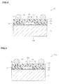
- FIGS. 9(A) to 9(C) illustrate an example configuration of an elastic wave device.
- FIG. 9(A) is a cross-sectional view
- FIG. 9(B) is a cross-section taken along line X-X in FIG. 9(A) viewed from above
- FIG. 9(C) is a cross-section taken along line X-X in FIG. 9(A) viewed from below.
- FIGS. 9(A) is a cross-sectional view
- FIG. 9(B) is a cross-section taken along line X-X in FIG. 9(A) viewed from above
- FIG. 9(C) is a cross-section taken along line X-X in FIG. 9(A) viewed from below.
- FIGS. 9(A) is a cross-sectional view
- FIG. 9(B) is a cross-section taken along line X-X in FIG. 9(A) viewed from above
- FIG. 9(C) is a cross-section taken along line X-
- a surface acoustic wave device 110 includes a piezoelectric substrate 111, a conductive pattern including IDT electrodes 112, pads 113, and wiring lines 118 formed on a first main surface 111a of the piezoelectric substrate, a frame-shaped supporting layer 116 composed of resin formed so as to enclose a vibrating portion including the IDT electrodes 112, and a cover layer 115 formed of an insulating sheet formed on the supporting layer 116.
- External electrodes 117 are formed on the cover layer 115, and the external electrodes 117 and the pads 113 are electrically connected to each other by via conductors 114 extending through the cover layer 115 and the supporting layer 116 (for example, see Patent Document 1).
- Patent Document 1 Japanese Unexamined Patent Application Publication No. 2002-261582
- the present invention provides an elastic wave device having a structure with which flux does not flow into a hollow space of the device during mounting of the device using solder bumps.
- the present invention provides an elastic wave device having the following structure.
- An elastic wave device includes (a) a substrate; (b) a vibrating portion formed on a first main surface of the substrate; (c) a pad formed on the first main surface of the substrate and electrically connected to an electrode of the vibrating portion; (d) a supporting layer having a thickness larger than that of the vibrating portion and formed on the first main surface of the substrate so as to enclose the vibrating portion; (e) a sheet-like cover layer composed of resin including synthetic rubber, formed on the supporting layer so as to cover the vibrating portion and to form a hollow 6+3..3+3+space around the periphery of the vibrating portion; (f) a protective layer composed of resin having resistance to flux, formed on a side of the cover layer remote from the supporting layer; (g) a via conductor extending through the protective layer, the cover layer, and the supporting layer and being connected to the pad; and (h) an external electrode formed of a solder bump, formed at an end of the via conductor adjacent to the protective layer.
- the flux is applied to the solder bump so as to improve solder wettability.
- the flux often flows into the hollow space.
- the inventors found that the flux passed through the cover layer since the cover layer was composed of resin including synthetic rubber. Synthetic rubber needs to be added to resin so that the cover layer has toughness and does not easily crack even when the cover layer has a sheet-like shape.
- the protective layer composed of resin having resistance to flux is formed on the sheet-like cover layer composed of resin including synthetic rubber as in the above-described structure, the flux does not pass through the protective layer. Accordingly, the flux can be prevented from flowing into the hollow space.
- the device can have various aspects as described below.
- the substrate may be a piezoelectric substrate.
- the vibrating portion may include an IDT electrode.
- the elastic wave device may be a surface acoustic wave device.
- the substrate may be an insulating substrate.
- the vibrating portion may include a piezoelectric thin film having electrodes formed on both sides thereof.
- the elastic wave device may be a bulk acoustic wave device such as a bulk acoustic wave resonator (BAW resonator).
- BAW resonator bulk acoustic wave resonator
- the protective layer is composed of the same material as the supporting layer.
- the protective layer is composed of the same material as the supporting layer, the variety of materials can be reduced, and manufacturing processes can be simplified.
- the protective layer is composed of photosensitive polyimide resin.
- the elastic wave device can be mounted with higher accuracy compared with when the external shape of the elastic wave device is recognized.
- the cover layer is composed of non-photosensitive epoxy resin.
- the device further includes a nitride film or an oxide film at least partially interposed between the substrate and the supporting layer.
- the nitride film or the oxide film has a surface rougher than that of the piezoelectric substrate. Therefore, adhesiveness can be improved by an anchoring effect. With this, problems that cause poor characteristics during processes after the formation of the hollow space, for example, entering of plating solution into the hollow space can be prevented.
- the present invention provides a method for manufacturing an elastic wave device as described below.
- a method for manufacturing an elastic wave device includes (1) a first step of forming a vibrating portion and a pad electrically connected to an electrode of the vibrating portion on a first main surface of a substrate; (2) a second step of forming a supporting layer having a thickness larger than that of the vibrating portion on the first main surface of the substrate so as to enclose the vibrating portion; (3) a third step of forming a sheet-like cover layer composed of resin including synthetic rubber on the supporting layer so as to cover the vibrating portion and to form a hollow space around the periphery of the vibrating portion; (4) a fourth step of forming a protective layer composed of resin having resistance to flux on a side of the cover layer remote from the supporting layer; (5) a fifth step of forming a via conductor extending through the protective layer, the cover layer, and the supporting layer and connected to the pad; and (6) a sixth step of forming an external electrode formed of a solder bump at an end of the via conductor remote from the protective layer.
- flux is applied to the solder bump so as to improve solder wettability.
- the flux often flows into the hollow space when only the cover layer is disposed on the hollow space since the flux passes through the cover layer composed of resin including synthetic rubber.
- the protective layer composed of resin having resistance to flux is formed on the cover layer as in the present invention, the flux does not pass through the protective layer composed of resin having resistance to flux, and can be prevented from flowing into the hollow space.
- the method includes (7) a seventh step of forming a groove in the substrate from the first main surface of the substrate to a predetermined depth; and (8) an eighth step of grinding a second main surface of the substrate opposite to the first main surface so as to reduce the thickness of the substrate and to divide the substrate into chips.
- a plurality of elastic wave devices having thinned substrate can be manufactured in a mother board at the same time while cracking caused by warpage of the substrate is prevented.
- chips are cut out by dicing after the second main surface of the substrate remote from the hollow space is ground until the substrate is reduced to a desired thickness.
- stress remaining in, for example, the supporting layer and the cover layer that form the hollow space disadvantageously causes high warpage and cracking of the substrate when the thickness thereof is reduced.
- the substrate having the hollow space the substrate does not significantly warp at the moment when the thickness thereof is reduced when a groove is cut from the first main surface of the substrate to a predetermined position in advance and the thickness of the substrate is reduced by grinding the second main surface. Therefore, cracking caused by the warpage of the substrate can be prevented.
- the supporting layer, the cover layer, and the protective layer can be cut when the groove is formed in the substrate.
- the substrate can be divided into chips by reducing the thickness of the substrate until the second main surface reaches the groove or by folding the substrate along the groove after the thickness of the substrate is reduced until the second main surface reaches to just short of the groove.
- the present invention provides a method for manufacturing an elastic wave device as described below.
- a method for manufacturing an elastic wave device includes (1) a first step of forming a vibrating portion and a pad electrically connected to an electrode of the vibrating portion on a first main surface of a substrate; (2) a second step of forming a supporting layer having a thickness larger than that of the vibrating portion on the first main surface of the substrate so as to enclose the vibrating portion; (3) a third step of forming a sheet-like multiple layer formed of a sheet-like cover layer composed of resin including synthetic rubber and a protective layer composed of resin having resistance to flux stacked in advance on the supporting layer such that the protective layer is located on a surface of the cover layer remote from the supporting layer so as to cover the vibrating portion and to form a hollow space around the periphery of the vibrating portion; (4) a fourth step of forming a via conductor extending through the protective layer and the cover layer of the multiple layer and the supporting layer and connected to the pad; and (5) a fifth step of forming an external electrode formed of a solder bump at an end of the via conductor
- flux is applied to the solder bump so as to improve solder wettability.
- the flux often flows into the hollow space when only the cover layer is disposed on the hollow space since the flux passes through the cover layer composed of resin including synthetic rubber.
- the protective layer composed of resin having resistance to flux is formed on the cover layer as in the present invention, the flux does not pass through the protective layer composed of resin having resistance to flux, and can be prevented from flowing into the hollow space.
- the method includes (6) a sixth step of forming a groove in the substrate from the first main surface of the substrate to a predetermined depth; and (7) a seventh step of grinding a second main surface of the substrate opposite to the first main surface so as to reduce the thickness of the substrate and to divide the substrate into chips.
- a plurality of elastic wave devices having thinned substrate can be manufactured in a mother board at the same time while cracking caused by warpage of the substrate is prevented.
- chips are cut out by dicing after the second main surface of the substrate remote from the hollow space is ground until the substrate is reduced to a desired thickness.
- stress remaining in, for example, the supporting layer and the cover layer that form the hollow space disadvantageously causes high warpage and cracking of the substrate when the thickness thereof is reduced.
- the substrate having the hollow space the substrate does not significantly warp at the moment when the thickness thereof is reduced when a groove is cut from the first main surface of the substrate to a predetermined position in advance and the thickness of the substrate is reduced by grinding the second main surface. Therefore, cracking caused by the warpage of the substrate can be prevented.
- the supporting layer, the cover layer, and the protective layer can be cut when the groove is formed in the substrate.
- the substrate can be divided into chips by reducing the thickness of the substrate until the second main surface reaches the groove or by folding the substrate along the groove after the thickness of the substrate is reduced until the second main surface reaches to just short of the groove.
- a protective layer can prevent flux from flowing into a hollow space of an elastic wave device during mounting of the device using solder bumps.
- FIGS. 1 to 8 Examples serving as embodiments of the present invention will now be described with reference to FIGS. 1 to 8 .
- Example 1 An electronic component 30 of Example 1 will now be described with reference to FIGS. 1 to 4 and FIG. 8.
- an electronic component 30 of Example 1 includes two surface acoustic wave devices 10 mounted on an upper surface 40a serving as a first main surface of a common substrate 40. That is, lands 42 formed in the upper surface 40a of the common substrate 40 and the surface acoustic wave devices 10 are electrically connected to each other with solder bumps 18 interposed therebetween.
- a resin 32 is disposed over the surface acoustic wave devices 10 so as to cover the surface acoustic wave devices 10.
- External electrodes 44 used for mounting the electronic component 30 on, for example, other circuit boards are exposed at a lower surface 40b serving as a second main surface of the common substrate 40. Via conductors 46 and internal wiring patterns 48 that electrically connect the lands 42 and the external electrodes 44 are formed inside the common substrate 40.
- the electronic component 30 can be a duplexer, and can include the surface acoustic wave devices 10 as surface-acoustic-wave filter elements for transmission and reception mounted side by side on the common substrate 40.
- the surface acoustic wave devices 10 each include a piezoelectric substrate 11 and an element portion, for example, a SAW (surface acoustic wave) filter formed on the piezoelectric substrate. That is, an IDT (interdigital transducer) electrode 12 serving as a comb-shaped electrode of a vibrating portion 14, pads 13, and a conductive pattern including wiring lines (not shown) that connect the IDT electrode 12 and the pads 13 to each other are formed on an upper surface 11a serving as a first main surface of the piezoelectric substrate 11.
- a frame-shaped supporting layer 20 is formed so as to enclose the vibrating portion 14 including the IDT electrode 12. The thickness of the supporting layer 20 is larger than that of the conductive pattern such as the IDT electrode 12 of the vibrating portion 14.
- the supporting layer 20 is formed also on the pads 13.
- a cover layer 22 is disposed on the supporting layer 20, and the periphery of the vibrating portion 14 formed on the piezoelectric substrate 11 is covered with the supporting layer 20 and the cover layer 22 serving as insulating members, thereby forming a hollow space 19.
- Surface acoustic waves freely propagate along the upper surface 11a of the piezoelectric substrate 11 in a portion adjacent to the hollow space 19.
- a protective layer 24 is formed on the cover layer 22.
- Via holes (through-holes) 15 extending to the pads 13 formed on the upper surface 11a of the piezoelectric substrate 11 are formed in the protective layer 24, the cover layer 22, and the supporting layer 20.
- Under-bump metals 16 serving as via conductors are disposed in the via holes 15, and solder bumps 18 are formed on the under-bump metals 16 so as to be exposed to the outside.
- FIGS. 2(a) to 3(f) manufacturing processes of the surface acoustic wave device 10 will be described with reference to cross-sectional views in FIGS. 2(a) to 3(f) .
- a plurality of surface acoustic wave devices 10 are manufactured in a mother board (wafer) at the same time.
- the IDT electrode 12, the pads 13, and the conductive pattern including wiring lines (not shown) that connect the IDT electrode 12 and the pad 13 to each other are formed on the first main surface 11a of the piezoelectric substrate 11, and the supporting layer 20 is formed around the periphery of the vibrating portion 14 including the IDT electrode 12.
- photosensitive polyimide resin for example, is applied onto the entire first main surface 11a of the piezoelectric substrate 11, and the resin is opened (removed) at the periphery of the vibrating portion 14 including the IDT electrode 12 using a photolithographic technique.
- the sheet-like cover layer 22 is formed on the supporting layer 22 by, for example, lamination.
- the cover layer 22 is composed of, for example, non-photosensitive epoxy resin which allows a low temperature curing process.
- the protective layer 24 is formed on the cover layer 22.
- the protective layer 24 is composed of, for example, photosensitive polyimide resin, which is the same material as the supporting layer 20.
- the cover layer 22 and the protective layer 24 can be formed at the same time by placing a sheet-like multiple layer including a sheet to be the cover layer 22 and a sheet to be the protective layer 24 stacked in advance on the supporting layer 20 instead of stacking the protective layer 24 after stacking the cover layer 22 on the supporting layer 20.
- the via holes 15 are formed by laser processing so as to extend through the protective layer 24, the cover layer 22, and the supporting layer 20 and such that the pads 13 at the bottoms of the via holes are exposed therethrough.
- the under-bump metals 16 serving as via conductors are formed in the via holes 15 by electrolytic plating (using, Cu, Ni, or the like), and Au for antioxidation having a thickness of about 0.05 to 0.1 ⁇ m is formed on surfaces 16a of the under-bump metals 16.
- solder paste such as Sn-Ag-Cu is printed immediately above the under-bump metals 16 with the metal masks interposed therebetween, and is heated at, for example, about 260 °C, at which the solder paste melts so that the solder becomes fixed to the under-bump metals 16. Flux is removed using a flux cleaner. With this, the spherical solder bumps 18 are formed.
- grooves are cut from the protective layer 24 to a predetermined depth in the piezoelectric substrate 11 by, for example, dicing, and the bottom surface (second main surface) 11b of the piezoelectric substrate 11 is ground so that the thickness of the substrate is reduced and thereby that the board is divided into chips.
- the supporting layer 20, the cover layer 22, and the protective layer 24 can be cut when the grooves are cut.
- the board can be divided into chips by reducing the thickness of the piezoelectric substrate 11 until the bottom surface reaches the grooves or by folding the piezoelectric substrate 11 along the grooves after the thickness of the piezoelectric substrate 11 is reduced until the bottom surface reaches to just short of the grooves.
- the bottom surface 11b of the substrate remote from the hollow space 19 is ground until the substrate is reduced to a desired thickness before chips are cut out by dicing.
- stress remaining in the resins such as the supporting layer 20 and the cover layer 22 that form the hollow space 19 disadvantageously causes high warpage and cracking of the piezoelectric substrate 11 serving as a mother board when the thickness thereof is reduced.
- the piezoelectric substrate 11 having the hollow space 19 the piezoelectric substrate 11 does not significantly warp at the moment when the thickness thereof is reduced when grooves are cut from the first main surface 11a of the piezoelectric substrate 11 to a predetermined position in advance and the thickness of the substrate is reduced by grinding the bottom surface 11b. Therefore, cracking caused by the warpage of the piezoelectric substrate 11 can be prevented.
- the surface acoustic wave devices 10 are mounted on a printed circuit board to be the common substrate 40.
- flux is applied to the solder bumps 18 so as to improve the solder wettability.
- the surface acoustic wave devices 10 are embedded in the resin 32 by, for example, lamination or resin molding while being pressurized at 2 to 5 Pa, and then the board is divided into chips. This completes the fabrication of the electronic component 30 shown in FIG. 1 .
- the thickness of the supporting layer 20 is 15 ⁇ m
- the thickness of the cover layer 22 is 30 ⁇ m
- the thickness of the protective layer 24 is 3 ⁇ m.
- the cover layer 22 can be a sheet of resin including synthetic rubber, for example, a sheet of non-photosensitive epoxy resin.
- the cover layer 22 has toughness even when it has a sheet-like shape due to the addition of the synthetic rubber, and does not crack easily.
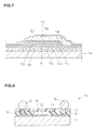
- solder bumps 18 are formed immediately above the cover layer 22 as in a surface acoustic wave device 10x shown in a cross-sectional view in FIG. 8 , flux often flows into the hollow space 19 through the cover layer 22 composed of resin including synthetic rubber such as acrylic rubber.
- the protective layer 24 composed of resin having resistance to flux is formed on the cover layer 22 as shown in FIG. 4 , and the solder bumps 18 are formed thereon. With this, flux does not pass through the protective layer 24 composed of resin having resistance to flux, and can be prevented from flowing into the hollow space 19.
- the material of the protective layer 24 can differ from that of the supporting layer 20, the material of the protective layer 24 is preferably the same as that of the supporting layer 20 when the supporting layer 20 is composed of resin having resistance to flux since the variety of materials is not increased and thereby manufacturing processes can be simplified.
- the surface acoustic wave devices 10 can be improved by mounting the devices by recognizing the solder bumps 18 rather than mounting the devices by recognizing the external shapes of the devices, the shape being affected by dicing accuracy.
- the protective layer 24 is composed of the same photosensitive polyimide resin as the supporting layer 20, a difference in brightness profile between the solder bumps 18 and the protective layer 24 becomes large, and it becomes easy for the solder bump 18 to be recognized. Accordingly, the surface acoustic wave devices 10 can be mounted with higher accuracy compared with when the external shapes of the surface acoustic wave devices 10 are recognized.
- the hollow space 19 is hermetically sealed by the resin 32.
- the protective layer 24 is not intended to hermetically seal the hollow space 19.
- Openings for the via holes can be formed in the supporting layer 20 such that the pads 13 are at least partially exposed when the supporting layer is formed.
- part of the material (for example, filler) of the cover layer adheres to the bottoms of the via holes, i.e., the pads, and adversely affects adhesiveness between the pads and the platings subsequently disposed in the via holes.
- the openings for the via holes are not formed in the supporting layer during the formation of the supporting layer and the via holes are formed in the supporting layer, the cover layer, and the protective layer by laser processing at the same time after the formation of the cover layer and the protective layer, the above-described problem does not occur, and adhesiveness between the pads and the platings disposed in the via holes can be improved.
- the size of the hollow space 19 required to realize a SAW filter used in an 800 MHz band, which requires the largest size in frequency bands in which general SAW filters are used, is 400 ⁇ m ⁇ 1000 ⁇ m.
- the parameters of the supporting layer 20 and the cover layer 22 can be selected so as to satisfy the following conditions.
- the thickness of the protective layer 24 and the elastic modulus of the material of the protective layer 24 can be ignored as conditions to be adjusted so that the hollow space 19 does not collapse since the thickness of the protective layer 24 can be smaller than that of the cover layer 22.
- Example 2 A surface acoustic wave device 10a of Example 2 will now be described with reference to FIG. 5.
- the surface acoustic wave device 10a of Example 2 has the same structure as the surface acoustic wave device 10 of Example 1 except for the followings.
- an intermediate layer 26 is formed between the supporting layer 20 and the piezoelectric substrate 11.
- the intermediate layer 26 is formed in an area except for the portions of a vibrating portion 14a including the IDT electrode 12 and the pads 13 so as to enclose the vibrating portion 14a and to be interposed between the piezoelectric substrate 11 and the supporting layer 20.
- the intermediate layer 26 can improve adhesiveness.
- a SiO 2 film serving as the intermediate layer 26 is formed by, for example, forming the conductive pattern on the LiTaO 3 piezoelectric substrate 11 as in Example 1, forming the SiO 2 film on the substrate by sputtering, and then removing part of the SiO 2 film formed in portions from which the SiO 2 film is required to be removed, for example, the areas in which the vibrating portion 14a and the pads 13 are formed, by dry etching.
- a SiN film can be formed instead of the SiO 2 film.
- the supporting layer 20 and the like are formed as in Example 1.
- Adhesion strength can be improved by an anchoring effect since the SiO 2 film or the SiN film serving as the intermediate layer 26 has a surface rougher than that of the piezoelectric substrate 11.
- These films can be formed by sputtering or CVD (chemical vapor deposition).
- the hollow space 19 can be kept fluid-tight by forming the intermediate layer 26 between the piezoelectric substrate 11 and the supporting layer 20. With this, problems that cause poor characteristics during processes after the formation of the hollow space, for example, entering of plating solution into the hollow space 19 during plating of the via holes, can be prevented.
- the SiO 2 film can be removed such that the areas to be removed are larger than those of the pads 13.
- parts of the supporting layer 20 are also formed on the piezoelectric substrate 11 around the periphery of the pads 13.
- the intermediate layer 26 only needs to be interposed between the other parts of the supporting layer 20 and the piezoelectric substrate 11 and to enclose the vibrating portion 14a at a position closer to the IDT electrode 12 than the pads 13.
- Example 3 An electronic component 30x of Example 3 will now be described with reference to FIGS. 6 and 7.
- Example 3 As shown in a cross-sectional view in FIG. 6 , the electronic component 30x of Example 3 has substantially the same structure as the electronic component 30 of the Example 1. Only differences from Example 1 will be focused on in the following descriptions, and the same reference signs are used for components common to those in Example 1.
- the electronic component 30x of Example 3 includes the surface acoustic wave device 10 and a bulk acoustic wave device 10x mounted on the upper surface 40a serving as the first main surface of the common substrate 40. That is, the lands 42 formed in the upper surface 40a of the common substrate 40 are electrically connected to the surface acoustic wave device 10 and the bulk acoustic wave device 10x with the solder bumps 18 interposed therebetween.
- the resin 32 is disposed over the surface acoustic wave device 10 and the bulk acoustic wave device 10x so as to cover the surface acoustic wave device 10 and the bulk acoustic wave device 10x.
- the external electrodes 44 used for mounting the electronic component 30x on, for example, other circuit boards are exposed at the lower surface 40b serving as the second main surface of the common substrate 40.
- the via conductors 46 and the internal wiring patterns 48 that electrically connect the lands 42 and the external electrodes 44 are formed inside the common substrate 40.
- the electronic component 30x can be a duplexer, and can include the surface acoustic wave device 10 as a surface-acoustic-wave filter element and the bulk acoustic wave device 10x as a bulk-acoustic-wave filter element, one of which is for transmission and the other is for reception.
- the bulk acoustic wave device 10x has substantially the same structure as the surface acoustic wave device 10 of Example 1 except that a vibrating portion 14x is formed on an insulating substrate 11x composed of, for example, Si.
- the bulk acoustic wave device 10x has a package structure similar to that of the surface acoustic wave device 10.
- the bulk acoustic wave device 10x includes the frame-shaped supporting layer 20 formed on a first main surface 11s of the substrate 11x around the periphery of the vibrating portion 14x formed on the surface.
- the thickness of the supporting layer 20 is larger than that of the vibrating portion 14x.
- the supporting layer 20 is formed also on the pads 13.
- the cover layer 22 is disposed on the supporting layer 20, and the periphery of the vibrating portion 14x is covered with the supporting layer 20 and the cover layer 22 serving as insulating members, thereby forming the hollow space 19.
- the protective layer 24 is formed on the cover layer 22.
- the via holes (through-holes) 15 extending to the pads 13 are formed in the protective layer 24, the cover layer 22, and the supporting layer 20.
- the under-bump metals 16 serving as via conductors are disposed in the via holes 15, and the solder bumps 18 are formed on the under-bump metals 16 so as to be exposed to the outside.
- the above-described package structure is not limited to the bulk acoustic wave device of the SMR type of Example 3, and can also be applied to a bulk acoustic wave device in which a vibrating portion is disposed above a hollow formed in a substrate or in which a vibrating portion is supported while being suspended above a substrate by, for example, removing a dummy layer.
- the bulk acoustic wave device 10x includes the vibrating portion 14x including an upper electrode 12a, a lower electrode 12b, and a piezoelectric thin film 12s interposed therebetween unlike the surface acoustic wave device 10 of Example 1.
- the vibrating portion 14x is acoustically separated from the insulating substrate 11x by a reflector 17 interposed therebetween.
- the reflector 17 includes low acoustic impedance layers 17s with a relatively low acoustic impedance and high acoustic impedance layers 17t with a relatively high acoustic impedance alternately stacked on the insulating substrate 11x.
- the upper electrode 12a and the lower electrode 12b are electrically connected to the pads 13 (not shown in FIG. 7 ).
- the pads 13 can be directly formed on the main surface 11s of the insulating substrate 11x, or can be formed on the main surface 11s of the insulating substrate 11x with another layer (for example, a low acoustic impedance layer 17s) interposed therebetween.
- the SAW filter not only the SAW filter but also an element portion such as a SAW resonator can be formed on the piezoelectric substrate.
- an element portion such as a SAW resonator can be formed on the insulating substrate.
Landscapes
- Physics & Mathematics (AREA)
- Acoustics & Sound (AREA)
- Engineering & Computer Science (AREA)
- Manufacturing & Machinery (AREA)
- Surface Acoustic Wave Elements And Circuit Networks Thereof (AREA)
- Structures Or Materials For Encapsulating Or Coating Semiconductor Devices Or Solid State Devices (AREA)
Applications Claiming Priority (2)
| Application Number | Priority Date | Filing Date | Title |
|---|---|---|---|
| JP2008036396 | 2008-02-18 | ||
| PCT/JP2009/050666 WO2009104438A1 (ja) | 2008-02-18 | 2009-01-19 | 弾性波装置及びその製造方法 |
Publications (2)
| Publication Number | Publication Date |
|---|---|
| EP2246979A1 true EP2246979A1 (de) | 2010-11-03 |
| EP2246979A4 EP2246979A4 (de) | 2014-03-05 |
Family
ID=40985325
Family Applications (1)
| Application Number | Title | Priority Date | Filing Date |
|---|---|---|---|
| EP09711950.7A Withdrawn EP2246979A4 (de) | 2008-02-18 | 2009-01-19 | Elastische wellenvorrichtung und herstellungsverfahren dafür |
Country Status (5)
| Country | Link |
|---|---|
| US (2) | US8461940B2 (de) |
| EP (1) | EP2246979A4 (de) |
| JP (1) | JP5077714B2 (de) |
| CN (1) | CN101946409B (de) |
| WO (1) | WO2009104438A1 (de) |
Families Citing this family (42)
| Publication number | Priority date | Publication date | Assignee | Title |
|---|---|---|---|---|
| US9425764B2 (en) | 2012-10-25 | 2016-08-23 | Avago Technologies General Ip (Singapore) Pte. Ltd. | Accoustic resonator having composite electrodes with integrated lateral features |
| US9083302B2 (en) | 2011-02-28 | 2015-07-14 | Avago Technologies General Ip (Singapore) Pte. Ltd. | Stacked bulk acoustic resonator comprising a bridge and an acoustic reflector along a perimeter of the resonator |
| US9148117B2 (en) | 2011-02-28 | 2015-09-29 | Avago Technologies General Ip (Singapore) Pte. Ltd. | Coupled resonator filter comprising a bridge and frame elements |
| US9136818B2 (en) | 2011-02-28 | 2015-09-15 | Avago Technologies General Ip (Singapore) Pte. Ltd. | Stacked acoustic resonator comprising a bridge |
| JP2012182604A (ja) * | 2011-03-01 | 2012-09-20 | Panasonic Corp | 弾性波フィルタ部品 |
| US9490771B2 (en) | 2012-10-29 | 2016-11-08 | Avago Technologies General Ip (Singapore) Pte. Ltd. | Acoustic resonator comprising collar and frame |
| US9444426B2 (en) | 2012-10-25 | 2016-09-13 | Avago Technologies General Ip (Singapore) Pte. Ltd. | Accoustic resonator having integrated lateral feature and temperature compensation feature |
| US9490418B2 (en) | 2011-03-29 | 2016-11-08 | Avago Technologies General Ip (Singapore) Pte. Ltd. | Acoustic resonator comprising collar and acoustic reflector with temperature compensating layer |
| US9401692B2 (en) | 2012-10-29 | 2016-07-26 | Avago Technologies General Ip (Singapore) Pte. Ltd. | Acoustic resonator having collar structure |
| US9590165B2 (en) | 2011-03-29 | 2017-03-07 | Avago Technologies General Ip (Singapore) Pte. Ltd. | Acoustic resonator comprising aluminum scandium nitride and temperature compensation feature |
| US9484882B2 (en) | 2013-02-14 | 2016-11-01 | Avago Technologies General Ip (Singapore) Pte. Ltd. | Acoustic resonator having temperature compensation |
| JP5561254B2 (ja) * | 2011-07-29 | 2014-07-30 | 株式会社村田製作所 | 回路モジュール及び複合回路モジュール |
| JP2013055244A (ja) * | 2011-09-05 | 2013-03-21 | Murata Mfg Co Ltd | 電子部品及びその製造方法 |
| WO2013121866A1 (ja) | 2012-02-14 | 2013-08-22 | 株式会社村田製作所 | 電子部品素子およびそれを備えた複合モジュール |
| JP5807715B2 (ja) | 2012-03-23 | 2015-11-10 | 株式会社村田製作所 | 弾性波フィルタ素子及びその製造方法 |
| KR101645172B1 (ko) | 2012-09-25 | 2016-08-03 | 가부시키가이샤 무라타 세이사쿠쇼 | 탄성파 장치 및 그 제조 방법 |
| US9209380B2 (en) * | 2013-03-08 | 2015-12-08 | Triquint Semiconductor, Inc. | Acoustic wave device |
| WO2015098694A1 (ja) * | 2013-12-26 | 2015-07-02 | 株式会社村田製作所 | 弾性波装置及びその製造方法 |
| JP5907195B2 (ja) * | 2014-02-27 | 2016-04-26 | 株式会社村田製作所 | 電子部品及び電子部品の製造方法 |
| US9857685B2 (en) | 2014-06-13 | 2018-01-02 | Nippon Kayaku Kabushiki Kaisha | Photosensitive resin composition, resist laminate, cured product of photosensitive resin composition, and cured product of resist laminate (11) |
| KR101987712B1 (ko) | 2014-12-04 | 2019-06-11 | 가부시키가이샤 무라타 세이사쿠쇼 | 탄성파 장치의 제조 방법 및 탄성파 장치 |
| KR101959455B1 (ko) * | 2015-03-16 | 2019-03-18 | 가부시키가이샤 무라타 세이사쿠쇼 | 탄성 표면파 장치 |
| KR101931508B1 (ko) * | 2015-03-27 | 2018-12-21 | 가부시키가이샤 무라타 세이사쿠쇼 | 탄성파 장치, 통신 모듈 기기 및 탄성파 장치의 제조 방법 |
| WO2016189952A1 (ja) * | 2015-05-22 | 2016-12-01 | 株式会社村田製作所 | 電子部品 |
| CN107615657B (zh) | 2015-06-25 | 2020-12-01 | 株式会社村田制作所 | 弹性波装置 |
| WO2017098809A1 (ja) | 2015-12-11 | 2017-06-15 | 株式会社村田製作所 | 弾性波装置 |
| KR102653201B1 (ko) * | 2016-03-30 | 2024-04-01 | 삼성전기주식회사 | 음향파 디바이스 및 그 제조방법 |
| WO2017179574A1 (ja) | 2016-04-11 | 2017-10-19 | 株式会社村田製作所 | 弾性波素子および弾性波装置 |
| JP6715672B2 (ja) * | 2016-04-25 | 2020-07-01 | 株式会社村田製作所 | 回路モジュール |
| CN105866815B (zh) * | 2016-05-06 | 2018-12-28 | 中国工程物理研究院电子工程研究所 | 一种柔性结构的fbar伽马辐照传感器 |
| WO2018079007A1 (ja) * | 2016-10-28 | 2018-05-03 | 株式会社村田製作所 | 弾性波装置、高周波フロントエンド回路及び通信装置 |
| WO2018110464A1 (ja) * | 2016-12-15 | 2018-06-21 | 株式会社村田製作所 | 弾性波装置 |
| KR102414843B1 (ko) * | 2017-05-22 | 2022-06-30 | 삼성전기주식회사 | 음향파 디바이스 및 그 제조방법 |
| JP2019047363A (ja) * | 2017-09-04 | 2019-03-22 | 株式会社村田製作所 | 弾性波装置、高周波フロントエンド回路及び通信装置 |
| KR102550176B1 (ko) * | 2017-11-09 | 2023-07-03 | 삼성전기주식회사 | 음향파 디바이스 및 그 제조방법 |
| WO2019124126A1 (ja) * | 2017-12-22 | 2019-06-27 | 株式会社村田製作所 | 弾性波装置、高周波フロントエンド回路及び通信装置並びに弾性波装置の製造方法 |
| US11502067B2 (en) * | 2018-07-26 | 2022-11-15 | Advanced Semiconductor Engineering, Inc. | Package structure and method for manufacturing the same |
| CN112117979B (zh) * | 2019-08-16 | 2022-05-17 | 中芯集成电路(宁波)有限公司 | 谐振器及其制造方法、滤波器、电子设备 |
| WO2021241435A1 (ja) * | 2020-05-28 | 2021-12-02 | 株式会社村田製作所 | 弾性波装置 |
| US12334903B2 (en) * | 2020-08-31 | 2025-06-17 | Qualcomm Incorporated | Substrate comprising acoustic resonators configured as at least one acoustic filter |
| CN118337173B (zh) * | 2024-04-30 | 2025-12-02 | 泉州市三安集成电路有限公司 | 一种弹性波装置、芯片封装方法及射频模块 |
| CN118890024B (zh) * | 2024-07-19 | 2025-12-09 | 泉州市三安集成电路有限公司 | 弹性波器件及其制备方法 |
Family Cites Families (27)
| Publication number | Priority date | Publication date | Assignee | Title |
|---|---|---|---|---|
| JPS60189307A (ja) | 1984-03-09 | 1985-09-26 | Toshiba Corp | 圧電薄膜共振器およびその製造方法 |
| DE69718693T2 (de) * | 1996-03-08 | 2003-11-27 | Matsushita Electric Industrial Co., Ltd. | Elektronisches Bauteil und Herstellungsverfahren |
| GB0014630D0 (en) | 2000-06-16 | 2000-08-09 | Koninkl Philips Electronics Nv | Bulk accoustic wave filter |
| US6710682B2 (en) * | 2000-10-04 | 2004-03-23 | Matsushita Electric Industrial Co., Ltd. | Surface acoustic wave device, method for producing the same, and circuit module using the same |
| JP2002261582A (ja) | 2000-10-04 | 2002-09-13 | Matsushita Electric Ind Co Ltd | 弾性表面波デバイスおよびその製造方法ならびにそれを用いた回路モジュール |
| US6842812B1 (en) | 2000-11-02 | 2005-01-11 | Intel Corporation | Event handling |
| CN100350607C (zh) | 2001-12-07 | 2007-11-21 | 富士通株式会社 | 半导体器件及其制造方法 |
| CN1668980B (zh) * | 2002-07-11 | 2010-05-12 | 旭化成电子材料株式会社 | 高耐热性负型光敏树脂组合物 |
| JP2004129222A (ja) * | 2002-07-31 | 2004-04-22 | Murata Mfg Co Ltd | 圧電部品およびその製造方法 |
| JP4385607B2 (ja) * | 2003-01-29 | 2009-12-16 | セイコーエプソン株式会社 | 表面弾性波素子、周波数フィルタ、発振器、電子回路並びに電子機器 |
| EP1557880A1 (de) | 2004-01-21 | 2005-07-27 | Nitto Denko Corporation | Harzzusammensetzung um Halbleiter zu verkapseln |
| JP2005206664A (ja) | 2004-01-21 | 2005-08-04 | Nitto Denko Corp | 半導体封止用樹脂組成物 |
| JP2005303980A (ja) | 2004-03-15 | 2005-10-27 | Matsushita Electric Ind Co Ltd | 弾性表面波デバイスおよびその形成方法 |
| JP4492623B2 (ja) * | 2004-03-15 | 2010-06-30 | パナソニック株式会社 | 弾性表面波デバイスの製造方法 |
| JP4375399B2 (ja) * | 2004-07-20 | 2009-12-02 | 株式会社村田製作所 | 圧電フィルタ |
| JP5027509B2 (ja) * | 2004-08-18 | 2012-09-19 | 株式会社カネカ | 半導体封止剤用エポキシ樹脂組成物およびエポキシ樹脂成形材料 |
| JP4650018B2 (ja) * | 2005-02-17 | 2011-03-16 | 住友ベークライト株式会社 | ポリアミド樹脂及びポジ型感光性樹脂組成物並びにそれらを用いた半導体装置及び表示素子 |
| JP2006324894A (ja) * | 2005-05-18 | 2006-11-30 | Hitachi Media Electoronics Co Ltd | 表面弾性波デバイスおよびその製造方法 |
| JP4706907B2 (ja) * | 2005-06-15 | 2011-06-22 | 株式会社村田製作所 | 圧電デバイスとその製造方法 |
| JP2007019943A (ja) * | 2005-07-08 | 2007-01-25 | Alps Electric Co Ltd | 表面弾性波ディバイス |
| JP4908801B2 (ja) | 2005-08-16 | 2012-04-04 | 株式会社神戸製鋼所 | 電子部品用銅系基材及び電子部品 |
| JP4524474B2 (ja) * | 2005-11-17 | 2010-08-18 | 富士通メディアデバイス株式会社 | 弾性波デバイスおよびその製造方法 |
| JP4670872B2 (ja) * | 2006-01-18 | 2011-04-13 | 株式会社村田製作所 | 弾性表面波装置 |
| US9021669B2 (en) * | 2006-08-07 | 2015-05-05 | Kyocera Corporation | Method for manufacturing surface acoustic wave apparatus |
| JP5113394B2 (ja) * | 2007-01-23 | 2013-01-09 | 太陽誘電株式会社 | 弾性波デバイス |
| JP2009010559A (ja) * | 2007-06-27 | 2009-01-15 | Nippon Dempa Kogyo Co Ltd | 圧電部品及びその製造方法 |
| JP4503064B2 (ja) * | 2007-11-20 | 2010-07-14 | 日東電工株式会社 | 光導波路デバイスの製法およびそれによって得られる光導波路デバイス、並びにそれに用いられる光導波路接続構造 |
-
2009
- 2009-01-19 WO PCT/JP2009/050666 patent/WO2009104438A1/ja not_active Ceased
- 2009-01-19 CN CN200980104823.6A patent/CN101946409B/zh active Active
- 2009-01-19 JP JP2009554254A patent/JP5077714B2/ja active Active
- 2009-01-19 EP EP09711950.7A patent/EP2246979A4/de not_active Withdrawn
-
2010
- 2010-08-05 US US12/850,725 patent/US8461940B2/en active Active
-
2012
- 2012-08-10 US US13/571,386 patent/US20130205586A1/en not_active Abandoned
Also Published As
| Publication number | Publication date |
|---|---|
| CN101946409A (zh) | 2011-01-12 |
| WO2009104438A1 (ja) | 2009-08-27 |
| US20130205586A1 (en) | 2013-08-15 |
| US20100289600A1 (en) | 2010-11-18 |
| EP2246979A4 (de) | 2014-03-05 |
| US8461940B2 (en) | 2013-06-11 |
| JP5077714B2 (ja) | 2012-11-21 |
| JPWO2009104438A1 (ja) | 2011-06-23 |
| CN101946409B (zh) | 2014-08-20 |
Similar Documents
| Publication | Publication Date | Title |
|---|---|---|
| EP2246979A1 (de) | Elastische wellenvorrichtung und herstellungsverfahren dafür | |
| CN108292914B (zh) | 弹性波装置 | |
| US8552622B2 (en) | Acoustic wave device | |
| US7378922B2 (en) | Piezoelectric filter | |
| JP4460612B2 (ja) | 弾性表面波デバイス及びその製造方法 | |
| CN101232276B (zh) | 声波器件 | |
| US10840879B2 (en) | Surface acoustic wave device | |
| WO2016068096A1 (ja) | 受動素子付フィルタ部品および高周波モジュール | |
| KR102653201B1 (ko) | 음향파 디바이스 및 그 제조방법 | |
| US12176886B2 (en) | High-frequency apparatus | |
| CN107210727B (zh) | 电子部件 | |
| CN100546180C (zh) | 表面声波装置及其制造方法 | |
| JP2010278971A (ja) | 弾性波装置 | |
| CN111066241B (zh) | 滤波器装置 | |
| JP6433930B2 (ja) | 弾性波デバイス | |
| CN101192817A (zh) | 声波器件 | |
| KR100653089B1 (ko) | 탄성 표면파 디바이스 웨이퍼 레벨 패키지 및 그 패키징방법 | |
| US11626851B2 (en) | Acoustic wave device, high-frequency front end circuit, communication device, and method for manufacturing acoustic wave device | |
| US9941461B2 (en) | Electronic component element and composite module including the same | |
| KR102556333B1 (ko) | 표면 탄성파 웨이퍼 레벨 패키지 및 이를 위한 pcb 제작 방법 | |
| JP2004153412A (ja) | 弾性表面波装置及びその製造方法 | |
| US9621127B2 (en) | Elastic wave device with a bump defining a shield and manufacturing method thereof | |
| JP2009213174A (ja) | 弾性表面波装置、および実装構造体 | |
| JP4722204B2 (ja) | 弾性表面波装置及び弾性表面波装置の製造方法 | |
| JP4234088B2 (ja) | 電子部品及びその製造方法 |
Legal Events
| Date | Code | Title | Description |
|---|---|---|---|
| PUAI | Public reference made under article 153(3) epc to a published international application that has entered the european phase |
Free format text: ORIGINAL CODE: 0009012 |
|
| 17P | Request for examination filed |
Effective date: 20100806 |
|
| AK | Designated contracting states |
Kind code of ref document: A1 Designated state(s): AT BE BG CH CY CZ DE DK EE ES FI FR GB GR HR HU IE IS IT LI LT LU LV MC MK MT NL NO PL PT RO SE SI SK TR |
|
| AX | Request for extension of the european patent |
Extension state: AL BA RS |
|
| DAX | Request for extension of the european patent (deleted) | ||
| A4 | Supplementary search report drawn up and despatched |
Effective date: 20140131 |
|
| RIC1 | Information provided on ipc code assigned before grant |
Ipc: H03H 9/05 20060101ALI20140127BHEP Ipc: H03H 9/10 20060101AFI20140127BHEP |
|
| 17Q | First examination report despatched |
Effective date: 20170503 |
|
| GRAP | Despatch of communication of intention to grant a patent |
Free format text: ORIGINAL CODE: EPIDOSNIGR1 |
|
| INTG | Intention to grant announced |
Effective date: 20180820 |
|
| RAP1 | Party data changed (applicant data changed or rights of an application transferred) |
Owner name: MURATA MANUFACTURING CO., LTD. |
|
| RIN1 | Information on inventor provided before grant (corrected) |
Inventor name: TAKADA, NORIHIKO Inventor name: KADOI, ATSUSHI Inventor name: KUDO, HAYAMI |
|
| STAA | Information on the status of an ep patent application or granted ep patent |
Free format text: STATUS: THE APPLICATION IS DEEMED TO BE WITHDRAWN |
|
| 18D | Application deemed to be withdrawn |
Effective date: 20190103 |