EP2247959B1 - Integrierte frequenzkalibrationsarchitektur - Google Patents
Integrierte frequenzkalibrationsarchitektur Download PDFInfo
- Publication number
- EP2247959B1 EP2247959B1 EP09707492.6A EP09707492A EP2247959B1 EP 2247959 B1 EP2247959 B1 EP 2247959B1 EP 09707492 A EP09707492 A EP 09707492A EP 2247959 B1 EP2247959 B1 EP 2247959B1
- Authority
- EP
- European Patent Office
- Prior art keywords
- vco
- frequency
- voltage
- module
- dac
- Prior art date
- Legal status (The legal status is an assumption and is not a legal conclusion. Google has not performed a legal analysis and makes no representation as to the accuracy of the status listed.)
- Active
Links
Images


Classifications
-
- G—PHYSICS
- G01—MEASURING; TESTING
- G01S—RADIO DIRECTION-FINDING; RADIO NAVIGATION; DETERMINING DISTANCE OR VELOCITY BY USE OF RADIO WAVES; LOCATING OR PRESENCE-DETECTING BY USE OF THE REFLECTION OR RERADIATION OF RADIO WAVES; ANALOGOUS ARRANGEMENTS USING OTHER WAVES
- G01S7/00—Details of systems according to groups G01S13/00, G01S15/00, G01S17/00
- G01S7/02—Details of systems according to groups G01S13/00, G01S15/00, G01S17/00 of systems according to group G01S13/00
- G01S7/03—Details of HF subsystems specially adapted therefor, e.g. common to transmitter and receiver
- G01S7/032—Constructional details for solid-state radar subsystems
-
- G—PHYSICS
- G01—MEASURING; TESTING
- G01S—RADIO DIRECTION-FINDING; RADIO NAVIGATION; DETERMINING DISTANCE OR VELOCITY BY USE OF RADIO WAVES; LOCATING OR PRESENCE-DETECTING BY USE OF THE REFLECTION OR RERADIATION OF RADIO WAVES; ANALOGOUS ARRANGEMENTS USING OTHER WAVES
- G01S7/00—Details of systems according to groups G01S13/00, G01S15/00, G01S17/00
- G01S7/02—Details of systems according to groups G01S13/00, G01S15/00, G01S17/00 of systems according to group G01S13/00
- G01S7/35—Details of non-pulse systems
-
- G—PHYSICS
- G01—MEASURING; TESTING
- G01S—RADIO DIRECTION-FINDING; RADIO NAVIGATION; DETERMINING DISTANCE OR VELOCITY BY USE OF RADIO WAVES; LOCATING OR PRESENCE-DETECTING BY USE OF THE REFLECTION OR RERADIATION OF RADIO WAVES; ANALOGOUS ARRANGEMENTS USING OTHER WAVES
- G01S7/00—Details of systems according to groups G01S13/00, G01S15/00, G01S17/00
- G01S7/02—Details of systems according to groups G01S13/00, G01S15/00, G01S17/00 of systems according to group G01S13/00
- G01S7/40—Means for monitoring or calibrating
- G01S7/4004—Means for monitoring or calibrating of parts of a radar system
- G01S7/4008—Means for monitoring or calibrating of parts of a radar system of transmitters
-
- G—PHYSICS
- G01—MEASURING; TESTING
- G01S—RADIO DIRECTION-FINDING; RADIO NAVIGATION; DETERMINING DISTANCE OR VELOCITY BY USE OF RADIO WAVES; LOCATING OR PRESENCE-DETECTING BY USE OF THE REFLECTION OR RERADIATION OF RADIO WAVES; ANALOGOUS ARRANGEMENTS USING OTHER WAVES
- G01S13/00—Systems using the reflection or reradiation of radio waves, e.g. radar systems; Analogous systems using reflection or reradiation of waves whose nature or wavelength is irrelevant or unspecified
- G01S13/88—Radar or analogous systems specially adapted for specific applications
- G01S13/93—Radar or analogous systems specially adapted for specific applications for anti-collision purposes
- G01S13/931—Radar or analogous systems specially adapted for specific applications for anti-collision purposes of land vehicles
-
- H—ELECTRICITY
- H03—ELECTRONIC CIRCUITRY
- H03L—AUTOMATIC CONTROL, STARTING, SYNCHRONISATION OR STABILISATION OF GENERATORS OF ELECTRONIC OSCILLATIONS OR PULSES
- H03L2207/00—Indexing scheme relating to automatic control of frequency or phase and to synchronisation
- H03L2207/06—Phase locked loops with a controlled oscillator having at least two frequency control terminals
-
- H—ELECTRICITY
- H03—ELECTRONIC CIRCUITRY
- H03L—AUTOMATIC CONTROL, STARTING, SYNCHRONISATION OR STABILISATION OF GENERATORS OF ELECTRONIC OSCILLATIONS OR PULSES
- H03L7/00—Automatic control of frequency or phase; Synchronisation
- H03L7/06—Automatic control of frequency or phase; Synchronisation using a reference signal applied to a frequency- or phase-locked loop
- H03L7/08—Details of the phase-locked loop
- H03L7/099—Details of the phase-locked loop concerning mainly the controlled oscillator of the loop
Definitions
- Automotive radar products are typically made by assembling a number of discrete components on one or more printed circuit boards. This results in automotive radar products that are typically undesirably bulky. Additionally, current narrowband frequency modulated continuous wave (FMCW) automotive radar products transmit a signal with a frequency ramp in discrete frequency steps. The discrete frequency steps are created using a digital-to-analog converter (DAC) integrated circuit to tune a free-running voltage controlled oscillator (VCO).
- the DAC is generally located on a Digital Signal Processor (DSP) module and the tuning voltage is communicated from the DSP module to a separate printed circuit board containing the VCO. Unfortunately, traversing a board-to-board connection makes the tuning voltage more susceptible to noise.
- DSP Digital Signal Processor
- the VCO typically requires frequency calibration over a range of temperatures because the oscillator frequency varies with the temperature.
- a free running VCO is calibrated by comparing its frequency to the frequency of a second VCO, which is referred to herein as a calibration VCO.
- the calibration VCO is phase locked to a crystal oscillator to generate a reference frequency.
- a mixer translates the reference frequency to direct current (DC), causing an impulse in the baseband filter.
- the impulse can be observed using an analog-to-digital converter to determine the free-running oscillator's tuning voltage that corresponds to the reference frequency.
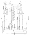
- a prior art FMCW radar system 100 comprises a transmit portion 110 and a receive portion(s) 120 of a radio frequency (RF) module 199. Furthermore, transmit portion 110 and receive portion(s) 120 are in communication with a digital signal processor (DSP) module 130.
- DSP digital signal processor
- the transmit and receive portions typically comprise discrete components. However, assembling the discrete components of RF module 199 results in an overall size increase in comparison to highly integrated circuit architecture.
- the typical design of radar system 100 includes a free running VCO 101 and a phase locked loop (PLL) architecture 150.
- a typical PLL architecture 150 comprises a calibrating VCO 152, a reference crystal oscillator (XSTL) 151, a PLL 153, and a loop filter 154.
- Calibrating VCO 152 operates at a known frequency due to being in a phase lock loop with XSTL 151.
- PLL architecture 150 is generally isolated from free running VCO 101 on RF module 199 because the output of calibrating VCO 152 is multiplied and operates at the same, or approximately the same, frequency as free running VCO 101. As is well known, having signals with similar frequencies in close proximity may result in signal interference and noise.
- one manner of tuning free running VCO 101 involves VCO tuning circuit on DSP module 130 comprising a pulse width modulator (PWM) 131 and a DAC 133.
- PWM pulse width modulator
- the VCO tuning circuit is adjusted based on a comparison of the output of VCO 101 and the multiplied output of calibration VCO 152.
- US5262957 discloses an inexpensive portable RF (radio frequency) microcontroller-based digital spectrum analyzer is automatically calibrated for passband amplitude tilt/variations. Resulting software-obtained calibration parameters are used during operation to reduce or eliminate passband amplitude errors.
- the spectrum analyzer also includes a PLL frequency synthesizer arrangement, but the PLL controls a VCO only during calibration to derive calibration values for controlling a digital-to-analog converter. During normal operation, the VCO is driven in an open loop configuration under software control using such calibration values-achieving nearly the accuracy of closed loop operation while avoiding the penalty of long PLL lock time.
- US6549078 discloses a method for generating a plurality of frequencies having predetermined frequency deviations from a phase lock loop device including a VCO having a main voltage input, a modulation voltage input and a frequency output, a first and second feedback loop digital divider, each having an input and an output, a phase frequency detector having a first and second input and an output, a reference frequency generator such as a crystal oscillator having an output, a first and second reference frequency digital divider, each having an input and an output, a loop filter having an input and an output, a switch having an input and a first and a second switched output, a hold circuit having an input and an output, a memory circuit for storing the a lock voltage and the corresponding loop output frequency.
- a VCO having a main voltage input, a modulation voltage input and a frequency output
- a first and second feedback loop digital divider each having an input and an output
- a phase frequency detector having a first and second input and an output
- a reference frequency generator such
- a free running VCO has two modes: a normal operating mode and a calibration mode.
- the frequency of the free running VCO is set to a desired calibration frequency using a phase lock loop and a tuning voltage is measured.
- the DAC voltage is compared to tuning voltage of the phase locked VCO.
- the DAC voltage is adjusted to determine a correct DAC setting to use that corresponds to the calibration frequency when the free running VCO returns to the normal operating mode.
- the offset voltage error of a difference amplifier can be measured and compensated for as part of the frequency calibration.
- a reference crystal oscillator used in the phase lock loop is located on a DSP module instead of on the RF module.
- the free running VCO is the only high frequency VCO on a radio frequency module.
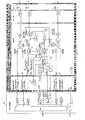
- a frequency calibration architecture 200 comprises an RF module 299 and a DSP module 230.
- RF module 299 is a printed circuit board (PCB).
- RF module 299 comprises a monolithic microwave integrated circuit (MMIC).
- MMIC monolithic microwave integrated circuit
- the RF module further comprises a free running VCO 201, a switch 205, a phase lock loop (PLL) 250, a difference amplifier 260, a transmit channel 210, and a receive channel(s) 220.
- the DSP module 230 may comprise a reference oscillator 206, and VCO tuning circuit of a PWM 231 and a DAC 233.
- the VCO tuning circuit may also comprise a low pass filter (LPF) 232
- reference oscillator 206 is a crystal oscillator. Furthermore, reference oscillator 206 may be located off-chip or on-chip. The crystal oscillator 206 is able to produce a precise frequency. In another exemplary embodiment, the crystal oscillator also provides the clock function of a DSP Module. In various embodiments, multiple crystal oscillators are present in the radar system.
- free running VCO 201 is a high frequency oscillator.
- the frequency of the oscillation is controlled by a tuning input voltage from a VCO tuning circuit.
- VCO 201 operates within the frequency range of about 22 GHz to about 29 GHz.
- VCO 201 operates within the frequency range of about 10 GHz to 45 GHz.
- VCO 201 may be a Hittite HMC533LP4.
- VCO 201 is the only high frequency VCO on RF module 299.
- frequency calibration architecture 200 may comprise any suitable VCO now known or hereinafter devised.
- the VCO tuning circuit is located on RF module 299, allowing for a digital connection between RF module 299 and the DSP module.
- the benefit of such a connection is that a digital board-to-board transmission is less susceptible to noise.
- the VCO tuning circuit is configured to provide both coarse tuning and fine tuning of VCO 201.
- the VCO needs to be tuned because the oscillation characteristics may drift, and/or vary with semiconductor process and temperature.
- Coarse tuning is facilitated by PWM 231 receiving a digital input signal from the DSP.
- the output of PWM 231 connects to VCO 201 after being added to the output of DAC 233.
- the output of PWM 231 passes through LPF 232 before reaching VCO 201.
- PWM 231 is replaced by a group of parallel capacitors 270 with switches to adjust resonant frequency and configured to perform coarse tuning on-chip.
- any suitable device(s) that perform coarse tuning on-chip may be used.
- fine tuning of VCO 201 is achieved by DAC 233, which also connects to the DSP to receive a digital input signal.
- the output of DAC 233 is in communication with a varactor diode in VCO 201.
- DAC 233 is designed on the same monolithic die as VCO 201.
- PLL 250 comprises a phase/frequency detector 253, a reference divider 255, a control counter 256, and a dual-modulus prescaler 257.
- dual-modulus prescaler 257 divides by factors of 32 and 33
- control counter 256 is a 5 & 11-bit counter.
- any suitable value(s) of dual-modulus prescaler 257 and control counter 256 may be used.
- PLL 250 further comprises a charge pump (not shown) which is associated with phase/frequency detector 253.
- switch 205 is configured to switch VCO 201 between the normal operating mode and the calibration mode. Furthermore, in one embodiment, the switch is controlled by a PLL ENABLE control line of the DSP. In an exemplary embodiment, and with reference to Figures 3 and 4 , control signals are communicated from DSP 230 through a serial peripheral interface (SPI) to RF module 299. In an exemplary embodiment, the control signals include the PLL ENABLE signal, a control signal for control counter 256, and a control signal for reference divider 255.
- SPI serial peripheral interface
- the VCO is connected to DAC 233, which may be on DSP module 230 or RF module 299.
- the VCO tuning circuit In the normal operation mode, the VCO tuning circuit generates a tuning voltage, which controls VCO 201.
- the tuning voltage is set by DSP 230, and corresponds to a desired VCO output frequency.
- a database or table is used to store output frequencies and corresponding tuning voltages.
- VCO 201 in the calibration mode, is connected to PLL 250 and disconnected from DAC 233, so that VCO 201 may be calibrated.
- frequency calibrating a free running VCO includes implementing a phase lock loop on the VCO at a programmed frequency.
- Dual-modulus prescaler 257 divides the VCO output frequency and transmits the reduced frequency output to phase/frequency detector 253.
- phase/frequency detector 253 receives a reference signal from reference oscillator 206.
- the reference signal passes through reference divider 255 prior to reaching phase/frequency detector 253.
- the reference divider 255 divides the reference frequency and allows for the reference frequency to be transmitted at a higher frequency from DSP module 230 to RF module 299. In an exemplary embodiment, transmitting across the board-to-board connection at a higher frequency results in less interference with other signals on DSP module 230.
- the phase/frequency detector 255 compares the reference signal to the reduced VCO output signal, and generates a voltage signal representing the phase difference of the two signal inputs.
- the PLL 250 automatically adjusts the input voltage of the VCO using the phase difference voltage signal.
- one of the steps to frequency calibrate is to compare a DAC voltage to the VCO tuning voltage after being phase locked at the programmed frequency.
- VCO 201 is connected to PLL 250
- the input voltage to VCO 201 is compared to the output voltage of DAC 233.
- the DAC communicates a signal through a low-pass filter 234 to a difference amplifier 260.
- the difference amplifier 260 compares the VCO input voltage and the voltage of the DAC, resulting in a Tuning Error that is transmitted to a DSP.
- the DAC voltage for a particular programmed frequency is determined when the DAC voltage is equal, or approximately equal to the VCO voltage.
- Adjusting the DAC voltage to equal or closely equal the VCO voltage provides the data point for a DAC voltage corresponding to the particular frequency during normal operation.
- the data point and programmed frequency are stored along with the corresponding DAC voltage to create a reference database.
- the error in measuring the Tuning Error voltage is taken into account during the calibration process.
- the DAC output voltage is adjusted to cause a Tuning Error output voltage of the DAC to be equal or approximately equal to the offset voltage measured in the normal mode.
- This adjustment of the DAC voltage allows the DAC to compensate for any offset voltage.
- the DAC compensates using difference amplifier 260 located on the integrated circuit of RF module 299 and an ADC located on DSP 230. Since in normal operation, the VCO tuning voltage is the same as the output voltage of the DAC, the offset voltage is measured by comparing the two.
- a frequency calibration table is populated using data points where the DAC voltage has been adjusted to compensate for the offset voltage of the VCO.
Landscapes
- Engineering & Computer Science (AREA)
- Radar, Positioning & Navigation (AREA)
- Remote Sensing (AREA)
- Computer Networks & Wireless Communication (AREA)
- Physics & Mathematics (AREA)
- General Physics & Mathematics (AREA)
- Stabilization Of Oscillater, Synchronisation, Frequency Synthesizers (AREA)
- Radar Systems Or Details Thereof (AREA)
- Transceivers (AREA)
- Inductance-Capacitance Distribution Constants And Capacitance-Resistance Oscillators (AREA)
- Semiconductor Integrated Circuits (AREA)
Claims (14)
- Integrierte Frequenzkalibrationsarchitektur, umfassend:ein Hochfrequenz-(HF)-Modul (299) in Kommunikation mit einem Digitalsignalprozessor-(DSP)-Modul (230), wobei sich das HF-Modul auf einer integrierten Schaltung befindet;einen spannungsgesteuerten Oszillator (VCO) (201) auf dem HF-Modul, wobei der VCO so konfiguriert ist, dass er einen Normalbetriebsmodus und einen Frequenzkalibrationsmodus aufweist;eine Phasenregelschleife (PLL) (250) auf dem HF-Modul, wobei die PLL eine VCO-Eingangsspannung für den VCO auf Grundlage einer skalierten Referenzfrequenz während des Frequenzkalibrationsmodus liefert;einen VCO-Abstimmungsschaltkreis, der einen Digital-analog-Umsetzer (DAC) (233) umfasst, wobei sich die DAC-Ausgangsspannung auf die VCO-Eingangsspannung während des Frequenzkalibrationsmodus reguliert, und wobei der DAC eine Verbindung mit dem VCO während des Normalbetriebsmodus hat;einen Schalter (205), der konfiguriert ist, um den VCO zwischen dem Normalbetriebsmodus und dem Frequenzkalibrationsmodus umzuschalten, undeinen Differenzverstärker (260) zum Vergleichen, während des Normalbetriebsmodus, der VCO-Eingangsspannung mit der regulierten DAC-Ausgangsspannung, um eine Offsetfehlerspannung zu erzeugern; undwobei die Architektur konfiguriert ist, um die regulierte DAC-Ausgangsspannung um die Offsetfehlerspannung zu korrigieren, um einen Offsetfehler des DACs zu kompensieren.
- Integrierte Frequenzkalibrationsarchitektur nach Anspruch 1, wobei der Schalter (205) durch ein Enable-Signal aus dem DSP-Modul (230) angesteuert wird.
- Integrierte Frequenzkalibrationsarchitektur nach Anspruch 1, wobei sich der VCO-Abstimmungsschaltkreis auf dem DSP-Modul befindet.
- Integrierte Frequenzkalibrationsarchitektur nach Anspruch 1, wobei sich der VCO-Abstimmungsschaltkreis auf dem HF-Modul befindet.
- Integrierte Frequenzkalibrationsarchitektur nach Anspruch 1, wobei die integrierte Schaltung eine monolisthisch integrierte Schaltung für den Mikrowellenbereich (MMIC) ist, wobei die MMIC eine integrierte Radar-Sende-/Empfangs-Schaltung ist.
- Integrierte Frequenzkalibrationsarchitektur nach Anspruch 1, die weiterhin eine Datenbank umfasst, die zur Speicherung einer Oszillationsfrequenz des VCOs und einer entsprechenden Abstimmungsspannung des DACs konfiguriert ist, wobei der VCO ein Hochfrequenz-VCO mit 10 GHz oder mehr ist, und wobei der VCO der einzige Hochfrequenz-VCO auf dem HF-Modul ist.
- Integrierte Frequenzkalibrationsarchitektur nach Anspruch 1, wobei die PLL umfasst:einen Dual-Modulus-Vorteiler und einen Kontrollzähler, die konfiguriert sind, um eine VCO-Ausgangsfrequenz zu reduzieren, um eine reduzierte VCO-Ausgangsfrequenz zu erzeugen; undeinen Referenzteiler, der konfiguriert ist, um eine Referenzfrequenz aus einem Referenzoszillator zu empfangen und um die skalierte Referenzfrequenz zu erzeugen; undeinen Phasen-/Frequenzdetektor, der konfiguriert ist, um die skalierte Referenzfrequenz und die reduzierte VCO-Ausgangsfrequenz des VCOs zu vergleichen;wobei der Phasen-/Frequenzdetektor eine Differenzspannung ausgibt, die ausgelegt ist, um die VCO-Ausgangsfrequenz während des Frequenzkalibrationsmodus zu regulieren.
- Integrierte Frequenzkalibrationsarchitektur nach Anspruch 7, wobei der Referenzoszillator ein Kristalloszillator ist.
- Integrierte Frequenzkalibrationsarchitektur nach Anspruch 8, wobei sich der Kristalloszillator auf dem HF-Modul befindet.
- Integrierte Frequenzkalibrationsarchitektur nach Anspruch 8, wobei sich der Kristalloszillator nicht auf dem HF-Modul befindet, und wobei der Kristalloszillator ein Taktgeber für einen digitalen Signalprozessor ist.
- Verfahren zur Frequenzkalibration eines spannungsgesteuerten Oszillators (VCO) (201) auf einer integrierten Schaltung (299), wobei das Verfahren umfasst:phasenstarres Regeln, auf der integrierten Schaltung, des VCOs auf Grundlage einer Referenzfrequenz und einer VCO-Ausgangsfrequenz, und Erzeugen einer VCO-Eingangsspannung; undRegulieren einer Ausgangsspannung eines Digital-analog-Umsetzers (DAC) (233) während eines Frequenzkalibrationsmodus, damit sie mit der VCO-Eingangsspannung übereinstimmt und um eine regulierte DAC-Ausgangsspannung zu erzeugen;wobei die regulierte DAC-Ausgangsspannung die VCO-Eingangsspannung während eines Normalbetriebsmodus liefert;Vergleichen, während des Normalbetriebsmodus, der VCO-Eingangsspannung mit der regulierten DAC-Ausgangsspannung unter Verwendung eines Differenzverstärkers (260), wobei der Differenzverstärker eine Offsetfehlerspannung erzeugt; undKorrigieren der regulierten DAC-Ausgangsspannung um die Offsetfehlerspannung, wobei das Korrigieren ausgelegt ist, um einen Offsetfehler des DACs zu kompensieren.
- Verfahren nach Anspruch 11, das weiterhin das Korrigieren einer gespeicherten DAC-Ausgangsspannung um die Offsetfehlerspannung umfasst, und das Wiederholen des Verfahrens mit einer anderen Programmierfrequenz.
- Verfahren nach Anspruch 11, wobei die Referenzfrequenz durch einen Kristalloszillator erzeugt wird, und wobei der VCO ein Hochfrequenz-VCO mit 10 GHz oder mehr ist, und wobei der VCO der einzige Hochfrequenz-VCO auf einem Hochfrequenz-(HF)-Modul ist.
- Verfahren nach Anspruch 11, wobei die regulierte DAC-Ausgangsspannung und die entsprechende VCO-Ausgangsfrequenz in einer Referenztabelle gespeichert werden in Reaktion darauf, dass die regulierte DAC-Ausgangsspannung im Wesentlichen gleich der VCO-Eingangsspannung auf Grundlage der Referenzfrequenz ist.
Applications Claiming Priority (2)
| Application Number | Priority Date | Filing Date | Title |
|---|---|---|---|
| US2555908P | 2008-02-01 | 2008-02-01 | |
| PCT/US2009/032672 WO2009099953A1 (en) | 2008-02-01 | 2009-01-30 | Integrated frequency calibration architecture |
Publications (2)
| Publication Number | Publication Date |
|---|---|
| EP2247959A1 EP2247959A1 (de) | 2010-11-10 |
| EP2247959B1 true EP2247959B1 (de) | 2014-03-26 |
Family
ID=40672313
Family Applications (3)
| Application Number | Title | Priority Date | Filing Date |
|---|---|---|---|
| EP09707492.6A Active EP2247959B1 (de) | 2008-02-01 | 2009-01-30 | Integrierte frequenzkalibrationsarchitektur |
| EP14163942.7A Active EP2762913B1 (de) | 2008-02-01 | 2009-01-30 | Hochintegrierte Schaltungsarchitektur |
| EP09708419A Withdrawn EP2247958A2 (de) | 2008-02-01 | 2009-01-30 | Hochintegrierte schaltungsarchitektur |
Family Applications After (2)
| Application Number | Title | Priority Date | Filing Date |
|---|---|---|---|
| EP14163942.7A Active EP2762913B1 (de) | 2008-02-01 | 2009-01-30 | Hochintegrierte Schaltungsarchitektur |
| EP09708419A Withdrawn EP2247958A2 (de) | 2008-02-01 | 2009-01-30 | Hochintegrierte schaltungsarchitektur |
Country Status (3)
| Country | Link |
|---|---|
| US (2) | US8044845B2 (de) |
| EP (3) | EP2247959B1 (de) |
| WO (2) | WO2009099952A2 (de) |
Families Citing this family (43)
| Publication number | Priority date | Publication date | Assignee | Title |
|---|---|---|---|---|
| EP2247959B1 (de) * | 2008-02-01 | 2014-03-26 | ViaSat, Inc. | Integrierte frequenzkalibrationsarchitektur |
| WO2010092438A1 (en) * | 2009-02-13 | 2010-08-19 | Freescale Semiconductor, Inc. | Integrated circuit comprising frequency generation circuitry for controlling a frequency source |
| US8704604B2 (en) * | 2009-12-23 | 2014-04-22 | Sand 9, Inc. | Oscillators having arbitrary frequencies and related systems and methods |
| US8604888B2 (en) * | 2009-12-23 | 2013-12-10 | Sand 9, Inc. | Oscillators having arbitrary frequencies and related systems and methods |
| US8228127B2 (en) | 2009-12-23 | 2012-07-24 | Sand 9, Inc. | Oscillators having arbitrary frequencies and related systems and methods |
| JP5307067B2 (ja) * | 2010-03-30 | 2013-10-02 | 古河電気工業株式会社 | 車載用パルスレーダ |
| DE102011115309A1 (de) * | 2011-09-29 | 2013-04-04 | Infineon Technologies Ag | Radarschaltung, Radarsystem und Verfahren zum Testen einer Verbindung zwischen einer Radarschaltung und einer Radarantenne in einem Fahrzeug |
| DE102012100427A1 (de) * | 2012-01-19 | 2013-07-25 | Hella Kgaa Hueck & Co. | Vorrichtung mit einem spannungsgesteuerten Oszillator und einer Schaltungsanordnung zum Ansteuern des Oszillators |
| DE102012106506A1 (de) * | 2012-07-18 | 2014-01-23 | Hella Kgaa Hueck & Co. | Verfahren zur Bestimmung der Funktionsfähigkeit eines schaltbaren Empfangsverstärkers |
| US20140027157A1 (en) * | 2012-07-26 | 2014-01-30 | Futurewei Technologies, Inc. | Device and Method for Printed Circuit Board with Embedded Cable |
| CN102915067B (zh) * | 2012-10-30 | 2014-08-06 | 中国科学技术大学 | 一种高精度偏置电压控制设备及直流稳压电源 |
| TWI486611B (zh) * | 2013-04-18 | 2015-06-01 | Wistron Neweb Corp | 車用雷達系統之雷達裝置 |
| CN104122556B (zh) * | 2013-04-24 | 2017-08-15 | 启碁科技股份有限公司 | 用于车用雷达系统的雷达装置 |
| US9488719B2 (en) * | 2014-05-30 | 2016-11-08 | Toyota Motor Engineering & Manufacturing North America, Inc. | Automotive radar sub-system packaging for robustness |
| US9685960B2 (en) * | 2014-07-31 | 2017-06-20 | Valeo Radar Systems, Inc. | Method and apparatus for generating a bit stream signal having a reduced output swing |
| TWI540787B (zh) | 2014-12-09 | 2016-07-01 | 啟碁科技股份有限公司 | 巴倫濾波器及射頻系統 |
| CN105742763B (zh) * | 2014-12-11 | 2019-01-01 | 启碁科技股份有限公司 | 巴伦滤波器及射频系统 |
| DE102015103149B4 (de) * | 2015-03-04 | 2024-06-06 | HELLA GmbH & Co. KGaA | Radarvorrichtung |
| DE102015107419A1 (de) * | 2015-05-12 | 2016-11-17 | HÜBNER GmbH & Co. KG | Radarvorrichtung |
| US10727848B2 (en) * | 2015-07-08 | 2020-07-28 | Analog Devices Global | Phase-locked loop having a multi-band oscillator and method for calibrating same |
| US9846228B2 (en) | 2016-04-07 | 2017-12-19 | Uhnder, Inc. | Software defined automotive radar systems |
| US9689967B1 (en) * | 2016-04-07 | 2017-06-27 | Uhnder, Inc. | Adaptive transmission and interference cancellation for MIMO radar |
| US10261179B2 (en) | 2016-04-07 | 2019-04-16 | Uhnder, Inc. | Software defined automotive radar |
| US10069465B2 (en) | 2016-04-21 | 2018-09-04 | Communications & Power Industries Llc | Amplifier control system |
| US9945935B2 (en) | 2016-04-25 | 2018-04-17 | Uhnder, Inc. | Digital frequency modulated continuous wave radar using handcrafted constant envelope modulation |
| US9772397B1 (en) | 2016-04-25 | 2017-09-26 | Uhnder, Inc. | PMCW-PMCW interference mitigation |
| US9954955B2 (en) | 2016-04-25 | 2018-04-24 | Uhnder, Inc. | Vehicle radar system with a shared radar and communication system |
| US9753121B1 (en) | 2016-06-20 | 2017-09-05 | Uhnder, Inc. | Power control for improved near-far performance of radar systems |
| US10295580B2 (en) | 2016-10-03 | 2019-05-21 | Analog Devices Global | On-chip measurement for phase-locked loop |
| US9971020B1 (en) | 2017-02-10 | 2018-05-15 | Uhnder, Inc. | Radar data buffering |
| WO2018146530A1 (en) | 2017-02-10 | 2018-08-16 | Uhnder, Inc. | Reduced complexity fft-based correlation for automotive radar |
| US11454697B2 (en) | 2017-02-10 | 2022-09-27 | Uhnder, Inc. | Increasing performance of a receive pipeline of a radar with memory optimization |
| US11105890B2 (en) | 2017-12-14 | 2021-08-31 | Uhnder, Inc. | Frequency modulated signal cancellation in variable power mode for radar applications |
| US12386029B2 (en) | 2018-01-29 | 2025-08-12 | Robert Bosch Gmbh | Millimeter wave automotive radar systems |
| US11474225B2 (en) | 2018-11-09 | 2022-10-18 | Uhnder, Inc. | Pulse digital mimo radar system |
| DE102019103514A1 (de) | 2019-02-12 | 2020-08-13 | Infineon Technologies Ag | Verarbeitung von Radarsignalen |
| US11681017B2 (en) | 2019-03-12 | 2023-06-20 | Uhnder, Inc. | Method and apparatus for mitigation of low frequency noise in radar systems |
| US11953615B2 (en) | 2020-01-13 | 2024-04-09 | Uhnder Inc. | Method and system for antenna array calibration for cross-coupling and gain/phase variations in radar systems |
| WO2021165459A1 (de) * | 2020-02-20 | 2021-08-26 | 2Pi-Labs Gmbh | Referenzoszillatoranordnung, radarsystem und synchronisationsverfahren |
| US11251822B1 (en) * | 2020-07-23 | 2022-02-15 | Xilinx, Inc. | Software defined radio (SDR) filter relaxation technique for multiple-input and multiple-output (MIMO) and large antenna array (LAA) applications |
| WO2023100108A1 (en) | 2021-12-02 | 2023-06-08 | Uhnder, Inc. | Radar system with enhanced processing for increased contrast ratio, improved angular separability and elimination of ghost targets |
| CN114630511B (zh) * | 2022-03-04 | 2024-03-19 | 中国航天科工集团八五一一研究所 | 一种双向变频一体化组件的实现方法 |
| US20240192314A1 (en) * | 2022-12-08 | 2024-06-13 | Stmicroelectronics International N.V. | Method and apparatus for reducing storage for proportional data |
Family Cites Families (25)
| Publication number | Priority date | Publication date | Assignee | Title |
|---|---|---|---|---|
| US3618091A (en) * | 1961-11-10 | 1971-11-02 | Sanders Associates Inc | Conical antenna system |
| US3452300A (en) * | 1965-08-11 | 1969-06-24 | Merrimac Research & Dev Inc | Four port directive coupler having electrical symmetry with respect to both axes |
| US3803514A (en) * | 1972-06-05 | 1974-04-09 | Cayuga Ass Inc | Microwave oscillator |
| DE3526363A1 (de) * | 1985-07-19 | 1987-01-22 | Siemens Ag | Verfahren zum herstellen eines einstellbaren frequenzgenerators |
| US4791421A (en) * | 1986-09-10 | 1988-12-13 | Westinghouse Electric Corp. | Transmit-receive module for phased-array antennas |
| US5262957A (en) * | 1990-11-09 | 1993-11-16 | Global Communications, Inc. | Inexpensive portable RF spectrum analyzer with calibration features |
| DE69729344T8 (de) * | 1996-04-03 | 2005-02-17 | Honda Giken Kogyo K.K. | Radarmodul und MMIC-Anordnung dafür |
| DE69920273T2 (de) * | 1998-11-12 | 2005-09-22 | Broadcom Corp., Irvine | Integrierte tunerarchitektur |
| US6696898B1 (en) * | 1998-11-12 | 2004-02-24 | Broadcom Corporation | Differential crystal oscillator |
| US6738601B1 (en) * | 1999-10-21 | 2004-05-18 | Broadcom Corporation | Adaptive radio transceiver with floating MOSFET capacitors |
| US7555263B1 (en) * | 1999-10-21 | 2009-06-30 | Broadcom Corporation | Adaptive radio transceiver |
| US7299006B1 (en) * | 1999-10-21 | 2007-11-20 | Broadcom Corporation | Adaptive radio transceiver |
| US7113744B1 (en) * | 1999-10-21 | 2006-09-26 | Broadcom Corporation | Adaptive radio transceiver with a power amplifier |
| US6549078B1 (en) | 2000-11-18 | 2003-04-15 | Ashvattha Semiconductor Inc. | Method and system for directly modulating a voltage controlled oscillator for use in frequency/phase modulated systems |
| US7148683B2 (en) * | 2001-10-25 | 2006-12-12 | Intematix Corporation | Detection with evanescent wave probe |
| US7183922B2 (en) * | 2002-03-18 | 2007-02-27 | Paratek Microwave, Inc. | Tracking apparatus, system and method |
| EP1490148A2 (de) * | 2002-04-01 | 2004-12-29 | Med-El Elektromedizinische Geräte GmbH | Verringerung der auswirkung von magnetischen und elektromagnetischen feldern auf den magneten und/oder die elektronik eines implantats |
| US8222721B2 (en) * | 2003-09-15 | 2012-07-17 | Silicon Laboratories Inc. | Integrated circuit suitable for use in radio receivers |
| EP1969388A1 (de) | 2005-09-23 | 2008-09-17 | California Institute Of Technology | Vollintegrierter mm-wellen-phasengruppenempfänger und -sender mit onchip-antennen |
| KR101025184B1 (ko) * | 2006-01-26 | 2011-03-31 | 니혼 뎀파 고교 가부시키가이샤 | Vco 구동 회로 및 주파수 합성기 |
| JP4699402B2 (ja) * | 2006-02-28 | 2011-06-08 | 日本電波工業株式会社 | 発振器及び周波数シンセサイザ |
| DE102006024457B4 (de) * | 2006-05-24 | 2014-06-05 | Infineon Technologies Ag | Integrierte Schaltung zum Senden und/oder Empfangen von Signalen |
| DE102006024458B4 (de) * | 2006-05-24 | 2016-04-14 | Infineon Technologies Ag | Integrierte Mehrfachmischer-Schaltung |
| US7573420B2 (en) * | 2007-05-14 | 2009-08-11 | Infineon Technologies Ag | RF front-end for a radar system |
| EP2247959B1 (de) * | 2008-02-01 | 2014-03-26 | ViaSat, Inc. | Integrierte frequenzkalibrationsarchitektur |
-
2009
- 2009-01-30 EP EP09707492.6A patent/EP2247959B1/de active Active
- 2009-01-30 EP EP14163942.7A patent/EP2762913B1/de active Active
- 2009-01-30 WO PCT/US2009/032670 patent/WO2009099952A2/en not_active Ceased
- 2009-01-30 EP EP09708419A patent/EP2247958A2/de not_active Withdrawn
- 2009-01-30 US US12/363,412 patent/US8044845B2/en active Active
- 2009-01-30 WO PCT/US2009/032672 patent/WO2009099953A1/en not_active Ceased
- 2009-01-30 US US12/363,436 patent/US7804369B2/en active Active
Also Published As
| Publication number | Publication date |
|---|---|
| EP2247958A2 (de) | 2010-11-10 |
| WO2009099953A1 (en) | 2009-08-13 |
| US20090195321A1 (en) | 2009-08-06 |
| EP2762913B1 (de) | 2018-11-21 |
| US7804369B2 (en) | 2010-09-28 |
| WO2009099952A2 (en) | 2009-08-13 |
| US8044845B2 (en) | 2011-10-25 |
| WO2009099952A3 (en) | 2009-10-15 |
| EP2762913A1 (de) | 2014-08-06 |
| US20090195440A1 (en) | 2009-08-06 |
| EP2247959A1 (de) | 2010-11-10 |
Similar Documents
| Publication | Publication Date | Title |
|---|---|---|
| EP2247959B1 (de) | Integrierte frequenzkalibrationsarchitektur | |
| US7701299B2 (en) | Low phase noise PLL synthesizer | |
| US5301367A (en) | Direct digital synthesizer for producing a modulated intermediate frequency in a radio apparatus | |
| US5034703A (en) | Frequency synthesizer | |
| US6844763B1 (en) | Wideband modulation summing network and method thereof | |
| CN101272142B (zh) | 频率合成器 | |
| US6670861B1 (en) | Method of modulation gain calibration and system thereof | |
| US7576614B2 (en) | Frequency independent control | |
| US20050280476A1 (en) | Filter control apparatus and filter system | |
| MXPA04008636A (es) | Tecnicas de calibracion para sintetizadores de frecuencia. | |
| US11693089B2 (en) | Apparatus and method for applying frequency calibration to local oscillator signal derived from reference clock output of active oscillator | |
| JPH08505508A (ja) | 自動周波数制御装置 | |
| US6246864B1 (en) | Wireless microphone use UHF band carrier FM transmitter | |
| US5570066A (en) | Method of programming a frequency synthesizer | |
| CN201270504Y (zh) | 频率合成器 | |
| EP1560336B1 (de) | Doppelzugriffsmodulator mit einem Frequenzsynthetisierer | |
| US8125255B2 (en) | PLL circuit | |
| US7459946B2 (en) | Circuit arrangement for generating a reference signal | |
| US10992304B2 (en) | Methods and apparatuses for digitally controlled oscillator frequency resolution control | |
| EP1271788B1 (de) | Schaltungen zur Funkkommunikation | |
| GB2373113A (en) | Improvements in or relating to fast frequency-hopping synthesisers | |
| US20020024393A1 (en) | Electronic circuit for and a method of controlling the output frequency of a frequency synthesizer | |
| CN119496507A (zh) | 锁相频率合成方法及装置、电子设备 |
Legal Events
| Date | Code | Title | Description |
|---|---|---|---|
| PUAI | Public reference made under article 153(3) epc to a published international application that has entered the european phase |
Free format text: ORIGINAL CODE: 0009012 |
|
| 17P | Request for examination filed |
Effective date: 20100825 |
|
| AK | Designated contracting states |
Kind code of ref document: A1 Designated state(s): AT BE BG CH CY CZ DE DK EE ES FI FR GB GR HR HU IE IS IT LI LT LU LV MC MK MT NL NO PL PT RO SE SI SK TR |
|
| AX | Request for extension of the european patent |
Extension state: AL BA RS |
|
| DAX | Request for extension of the european patent (deleted) | ||
| 17Q | First examination report despatched |
Effective date: 20120403 |
|
| REG | Reference to a national code |
Ref country code: DE Ref legal event code: R079 Ref document number: 602009022740 Country of ref document: DE Free format text: PREVIOUS MAIN CLASS: G01S0007400000 Ipc: G01S0007030000 |
|
| RIC1 | Information provided on ipc code assigned before grant |
Ipc: G01S 7/03 20060101AFI20130823BHEP Ipc: H03L 7/099 20060101ALI20130823BHEP Ipc: H03L 7/10 20060101ALI20130823BHEP Ipc: G01S 7/40 20060101ALI20130823BHEP |
|
| GRAP | Despatch of communication of intention to grant a patent |
Free format text: ORIGINAL CODE: EPIDOSNIGR1 |
|
| INTG | Intention to grant announced |
Effective date: 20131023 |
|
| GRAS | Grant fee paid |
Free format text: ORIGINAL CODE: EPIDOSNIGR3 |
|
| GRAA | (expected) grant |
Free format text: ORIGINAL CODE: 0009210 |
|
| AK | Designated contracting states |
Kind code of ref document: B1 Designated state(s): AT BE BG CH CY CZ DE DK EE ES FI FR GB GR HR HU IE IS IT LI LT LU LV MC MK MT NL NO PL PT RO SE SI SK TR |
|
| REG | Reference to a national code |
Ref country code: GB Ref legal event code: FG4D |
|
| REG | Reference to a national code |
Ref country code: CH Ref legal event code: EP |
|
| REG | Reference to a national code |
Ref country code: AT Ref legal event code: REF Ref document number: 659258 Country of ref document: AT Kind code of ref document: T Effective date: 20140415 |
|
| REG | Reference to a national code |
Ref country code: IE Ref legal event code: FG4D |
|
| REG | Reference to a national code |
Ref country code: DE Ref legal event code: R096 Ref document number: 602009022740 Country of ref document: DE Effective date: 20140508 |
|
| PG25 | Lapsed in a contracting state [announced via postgrant information from national office to epo] |
Ref country code: LT Free format text: LAPSE BECAUSE OF FAILURE TO SUBMIT A TRANSLATION OF THE DESCRIPTION OR TO PAY THE FEE WITHIN THE PRESCRIBED TIME-LIMIT Effective date: 20140326 Ref country code: NO Free format text: LAPSE BECAUSE OF FAILURE TO SUBMIT A TRANSLATION OF THE DESCRIPTION OR TO PAY THE FEE WITHIN THE PRESCRIBED TIME-LIMIT Effective date: 20140626 |
|
| REG | Reference to a national code |
Ref country code: AT Ref legal event code: MK05 Ref document number: 659258 Country of ref document: AT Kind code of ref document: T Effective date: 20140326 |
|
| REG | Reference to a national code |
Ref country code: NL Ref legal event code: VDEP Effective date: 20140326 |
|
| REG | Reference to a national code |
Ref country code: LT Ref legal event code: MG4D |
|
| PG25 | Lapsed in a contracting state [announced via postgrant information from national office to epo] |
Ref country code: SE Free format text: LAPSE BECAUSE OF FAILURE TO SUBMIT A TRANSLATION OF THE DESCRIPTION OR TO PAY THE FEE WITHIN THE PRESCRIBED TIME-LIMIT Effective date: 20140326 Ref country code: FI Free format text: LAPSE BECAUSE OF FAILURE TO SUBMIT A TRANSLATION OF THE DESCRIPTION OR TO PAY THE FEE WITHIN THE PRESCRIBED TIME-LIMIT Effective date: 20140326 |
|
| PG25 | Lapsed in a contracting state [announced via postgrant information from national office to epo] |
Ref country code: HR Free format text: LAPSE BECAUSE OF FAILURE TO SUBMIT A TRANSLATION OF THE DESCRIPTION OR TO PAY THE FEE WITHIN THE PRESCRIBED TIME-LIMIT Effective date: 20140326 Ref country code: LV Free format text: LAPSE BECAUSE OF FAILURE TO SUBMIT A TRANSLATION OF THE DESCRIPTION OR TO PAY THE FEE WITHIN THE PRESCRIBED TIME-LIMIT Effective date: 20140326 |
|
| PG25 | Lapsed in a contracting state [announced via postgrant information from national office to epo] |
Ref country code: EE Free format text: LAPSE BECAUSE OF FAILURE TO SUBMIT A TRANSLATION OF THE DESCRIPTION OR TO PAY THE FEE WITHIN THE PRESCRIBED TIME-LIMIT Effective date: 20140326 Ref country code: RO Free format text: LAPSE BECAUSE OF FAILURE TO SUBMIT A TRANSLATION OF THE DESCRIPTION OR TO PAY THE FEE WITHIN THE PRESCRIBED TIME-LIMIT Effective date: 20140326 Ref country code: BG Free format text: LAPSE BECAUSE OF FAILURE TO SUBMIT A TRANSLATION OF THE DESCRIPTION OR TO PAY THE FEE WITHIN THE PRESCRIBED TIME-LIMIT Effective date: 20140626 Ref country code: CZ Free format text: LAPSE BECAUSE OF FAILURE TO SUBMIT A TRANSLATION OF THE DESCRIPTION OR TO PAY THE FEE WITHIN THE PRESCRIBED TIME-LIMIT Effective date: 20140326 Ref country code: NL Free format text: LAPSE BECAUSE OF FAILURE TO SUBMIT A TRANSLATION OF THE DESCRIPTION OR TO PAY THE FEE WITHIN THE PRESCRIBED TIME-LIMIT Effective date: 20140326 Ref country code: IS Free format text: LAPSE BECAUSE OF FAILURE TO SUBMIT A TRANSLATION OF THE DESCRIPTION OR TO PAY THE FEE WITHIN THE PRESCRIBED TIME-LIMIT Effective date: 20140726 Ref country code: BE Free format text: LAPSE BECAUSE OF FAILURE TO SUBMIT A TRANSLATION OF THE DESCRIPTION OR TO PAY THE FEE WITHIN THE PRESCRIBED TIME-LIMIT Effective date: 20140326 Ref country code: CY Free format text: LAPSE BECAUSE OF FAILURE TO SUBMIT A TRANSLATION OF THE DESCRIPTION OR TO PAY THE FEE WITHIN THE PRESCRIBED TIME-LIMIT Effective date: 20140326 |
|
| PG25 | Lapsed in a contracting state [announced via postgrant information from national office to epo] |
Ref country code: AT Free format text: LAPSE BECAUSE OF FAILURE TO SUBMIT A TRANSLATION OF THE DESCRIPTION OR TO PAY THE FEE WITHIN THE PRESCRIBED TIME-LIMIT Effective date: 20140326 Ref country code: SK Free format text: LAPSE BECAUSE OF FAILURE TO SUBMIT A TRANSLATION OF THE DESCRIPTION OR TO PAY THE FEE WITHIN THE PRESCRIBED TIME-LIMIT Effective date: 20140326 Ref country code: ES Free format text: LAPSE BECAUSE OF FAILURE TO SUBMIT A TRANSLATION OF THE DESCRIPTION OR TO PAY THE FEE WITHIN THE PRESCRIBED TIME-LIMIT Effective date: 20140326 Ref country code: PL Free format text: LAPSE BECAUSE OF FAILURE TO SUBMIT A TRANSLATION OF THE DESCRIPTION OR TO PAY THE FEE WITHIN THE PRESCRIBED TIME-LIMIT Effective date: 20140326 |
|
| PG25 | Lapsed in a contracting state [announced via postgrant information from national office to epo] |
Ref country code: PT Free format text: LAPSE BECAUSE OF FAILURE TO SUBMIT A TRANSLATION OF THE DESCRIPTION OR TO PAY THE FEE WITHIN THE PRESCRIBED TIME-LIMIT Effective date: 20140728 |
|
| REG | Reference to a national code |
Ref country code: DE Ref legal event code: R097 Ref document number: 602009022740 Country of ref document: DE |
|
| PG25 | Lapsed in a contracting state [announced via postgrant information from national office to epo] |
Ref country code: DK Free format text: LAPSE BECAUSE OF FAILURE TO SUBMIT A TRANSLATION OF THE DESCRIPTION OR TO PAY THE FEE WITHIN THE PRESCRIBED TIME-LIMIT Effective date: 20140326 |
|
| PLBE | No opposition filed within time limit |
Free format text: ORIGINAL CODE: 0009261 |
|
| STAA | Information on the status of an ep patent application or granted ep patent |
Free format text: STATUS: NO OPPOSITION FILED WITHIN TIME LIMIT |
|
| 26N | No opposition filed |
Effective date: 20150106 |
|
| PG25 | Lapsed in a contracting state [announced via postgrant information from national office to epo] |
Ref country code: IT Free format text: LAPSE BECAUSE OF FAILURE TO SUBMIT A TRANSLATION OF THE DESCRIPTION OR TO PAY THE FEE WITHIN THE PRESCRIBED TIME-LIMIT Effective date: 20140326 |
|
| REG | Reference to a national code |
Ref country code: DE Ref legal event code: R097 Ref document number: 602009022740 Country of ref document: DE Effective date: 20150106 |
|
| PG25 | Lapsed in a contracting state [announced via postgrant information from national office to epo] |
Ref country code: SI Free format text: LAPSE BECAUSE OF FAILURE TO SUBMIT A TRANSLATION OF THE DESCRIPTION OR TO PAY THE FEE WITHIN THE PRESCRIBED TIME-LIMIT Effective date: 20140326 |
|
| REG | Reference to a national code |
Ref country code: CH Ref legal event code: PL |
|
| PG25 | Lapsed in a contracting state [announced via postgrant information from national office to epo] |
Ref country code: LU Free format text: LAPSE BECAUSE OF FAILURE TO SUBMIT A TRANSLATION OF THE DESCRIPTION OR TO PAY THE FEE WITHIN THE PRESCRIBED TIME-LIMIT Effective date: 20150130 |
|
| PG25 | Lapsed in a contracting state [announced via postgrant information from national office to epo] |
Ref country code: MC Free format text: LAPSE BECAUSE OF FAILURE TO SUBMIT A TRANSLATION OF THE DESCRIPTION OR TO PAY THE FEE WITHIN THE PRESCRIBED TIME-LIMIT Effective date: 20140326 |
|
| PG25 | Lapsed in a contracting state [announced via postgrant information from national office to epo] |
Ref country code: CH Free format text: LAPSE BECAUSE OF NON-PAYMENT OF DUE FEES Effective date: 20150131 Ref country code: LI Free format text: LAPSE BECAUSE OF NON-PAYMENT OF DUE FEES Effective date: 20150131 |
|
| REG | Reference to a national code |
Ref country code: IE Ref legal event code: MM4A |
|
| REG | Reference to a national code |
Ref country code: FR Ref legal event code: PLFP Year of fee payment: 8 |
|
| PG25 | Lapsed in a contracting state [announced via postgrant information from national office to epo] |
Ref country code: IE Free format text: LAPSE BECAUSE OF NON-PAYMENT OF DUE FEES Effective date: 20150130 |
|
| PG25 | Lapsed in a contracting state [announced via postgrant information from national office to epo] |
Ref country code: GR Free format text: LAPSE BECAUSE OF FAILURE TO SUBMIT A TRANSLATION OF THE DESCRIPTION OR TO PAY THE FEE WITHIN THE PRESCRIBED TIME-LIMIT Effective date: 20140627 |
|
| PG25 | Lapsed in a contracting state [announced via postgrant information from national office to epo] |
Ref country code: MT Free format text: LAPSE BECAUSE OF FAILURE TO SUBMIT A TRANSLATION OF THE DESCRIPTION OR TO PAY THE FEE WITHIN THE PRESCRIBED TIME-LIMIT Effective date: 20140326 |
|
| REG | Reference to a national code |
Ref country code: FR Ref legal event code: PLFP Year of fee payment: 9 |
|
| PG25 | Lapsed in a contracting state [announced via postgrant information from national office to epo] |
Ref country code: HU Free format text: LAPSE BECAUSE OF FAILURE TO SUBMIT A TRANSLATION OF THE DESCRIPTION OR TO PAY THE FEE WITHIN THE PRESCRIBED TIME-LIMIT; INVALID AB INITIO Effective date: 20090130 |
|
| PG25 | Lapsed in a contracting state [announced via postgrant information from national office to epo] |
Ref country code: TR Free format text: LAPSE BECAUSE OF FAILURE TO SUBMIT A TRANSLATION OF THE DESCRIPTION OR TO PAY THE FEE WITHIN THE PRESCRIBED TIME-LIMIT Effective date: 20140326 |
|
| REG | Reference to a national code |
Ref country code: FR Ref legal event code: PLFP Year of fee payment: 10 |
|
| PG25 | Lapsed in a contracting state [announced via postgrant information from national office to epo] |
Ref country code: MK Free format text: LAPSE BECAUSE OF FAILURE TO SUBMIT A TRANSLATION OF THE DESCRIPTION OR TO PAY THE FEE WITHIN THE PRESCRIBED TIME-LIMIT Effective date: 20140326 |
|
| REG | Reference to a national code |
Ref country code: DE Ref legal event code: R082 Ref document number: 602009022740 Country of ref document: DE Representative=s name: KILBURN & STRODE LLP, NL |
|
| P01 | Opt-out of the competence of the unified patent court (upc) registered |
Effective date: 20230529 |
|
| PGFP | Annual fee paid to national office [announced via postgrant information from national office to epo] |
Ref country code: GB Payment date: 20260127 Year of fee payment: 18 |
|
| PGFP | Annual fee paid to national office [announced via postgrant information from national office to epo] |
Ref country code: DE Payment date: 20260128 Year of fee payment: 18 |
|
| PGFP | Annual fee paid to national office [announced via postgrant information from national office to epo] |
Ref country code: FR Payment date: 20260126 Year of fee payment: 18 |