EP2249196A1 - Transflektive flüssigkristallanzeigeeinrichtung - Google Patents
Transflektive flüssigkristallanzeigeeinrichtung Download PDFInfo
- Publication number
- EP2249196A1 EP2249196A1 EP09717315A EP09717315A EP2249196A1 EP 2249196 A1 EP2249196 A1 EP 2249196A1 EP 09717315 A EP09717315 A EP 09717315A EP 09717315 A EP09717315 A EP 09717315A EP 2249196 A1 EP2249196 A1 EP 2249196A1
- Authority
- EP
- European Patent Office
- Prior art keywords
- liquid crystal
- comb
- electrode
- shaped electrode
- upper substrate
- Prior art date
- Legal status (The legal status is an assumption and is not a legal conclusion. Google has not performed a legal analysis and makes no representation as to the accuracy of the status listed.)
- Granted
Links
Images




Classifications
-
- G—PHYSICS
- G02—OPTICS
- G02F—OPTICAL DEVICES OR ARRANGEMENTS FOR THE CONTROL OF LIGHT BY MODIFICATION OF THE OPTICAL PROPERTIES OF THE MEDIA OF THE ELEMENTS INVOLVED THEREIN; NON-LINEAR OPTICS; FREQUENCY-CHANGING OF LIGHT; OPTICAL LOGIC ELEMENTS; OPTICAL ANALOGUE/DIGITAL CONVERTERS
- G02F1/00—Devices or arrangements for the control of the intensity, colour, phase, polarisation or direction of light arriving from an independent light source, e.g. switching, gating or modulating; Non-linear optics
- G02F1/01—Devices or arrangements for the control of the intensity, colour, phase, polarisation or direction of light arriving from an independent light source, e.g. switching, gating or modulating; Non-linear optics for the control of the intensity, phase, polarisation or colour
- G02F1/13—Devices or arrangements for the control of the intensity, colour, phase, polarisation or direction of light arriving from an independent light source, e.g. switching, gating or modulating; Non-linear optics for the control of the intensity, phase, polarisation or colour based on liquid crystals, e.g. single liquid crystal display cells
- G02F1/133—Constructional arrangements; Operation of liquid crystal cells; Circuit arrangements
- G02F1/1333—Constructional arrangements; Manufacturing methods
- G02F1/1335—Structural association of cells with optical devices, e.g. polarisers or reflectors
- G02F1/133553—Reflecting elements
- G02F1/133555—Transflectors
-
- G—PHYSICS
- G02—OPTICS
- G02F—OPTICAL DEVICES OR ARRANGEMENTS FOR THE CONTROL OF LIGHT BY MODIFICATION OF THE OPTICAL PROPERTIES OF THE MEDIA OF THE ELEMENTS INVOLVED THEREIN; NON-LINEAR OPTICS; FREQUENCY-CHANGING OF LIGHT; OPTICAL LOGIC ELEMENTS; OPTICAL ANALOGUE/DIGITAL CONVERTERS
- G02F1/00—Devices or arrangements for the control of the intensity, colour, phase, polarisation or direction of light arriving from an independent light source, e.g. switching, gating or modulating; Non-linear optics
- G02F1/01—Devices or arrangements for the control of the intensity, colour, phase, polarisation or direction of light arriving from an independent light source, e.g. switching, gating or modulating; Non-linear optics for the control of the intensity, phase, polarisation or colour
- G02F1/13—Devices or arrangements for the control of the intensity, colour, phase, polarisation or direction of light arriving from an independent light source, e.g. switching, gating or modulating; Non-linear optics for the control of the intensity, phase, polarisation or colour based on liquid crystals, e.g. single liquid crystal display cells
- G02F1/133—Constructional arrangements; Operation of liquid crystal cells; Circuit arrangements
- G02F1/1333—Constructional arrangements; Manufacturing methods
- G02F1/1343—Electrodes
- G02F1/134309—Electrodes characterised by their geometrical arrangement
- G02F1/134363—Electrodes characterised by their geometrical arrangement for applying an electric field parallel to the substrate, i.e. in-plane switching [IPS]
-
- G—PHYSICS
- G09—EDUCATION; CRYPTOGRAPHY; DISPLAY; ADVERTISING; SEALS
- G09G—ARRANGEMENTS OR CIRCUITS FOR CONTROL OF INDICATING DEVICES USING STATIC MEANS TO PRESENT VARIABLE INFORMATION
- G09G3/00—Control arrangements or circuits, of interest only in connection with visual indicators other than cathode-ray tubes
- G09G3/20—Control arrangements or circuits, of interest only in connection with visual indicators other than cathode-ray tubes for presentation of an assembly of a number of characters, e.g. a page, by composing the assembly by combination of individual elements arranged in a matrix no fixed position being assigned to or needed to be assigned to the individual characters or partial characters
- G09G3/34—Control arrangements or circuits, of interest only in connection with visual indicators other than cathode-ray tubes for presentation of an assembly of a number of characters, e.g. a page, by composing the assembly by combination of individual elements arranged in a matrix no fixed position being assigned to or needed to be assigned to the individual characters or partial characters by control of light from an independent source
- G09G3/36—Control arrangements or circuits, of interest only in connection with visual indicators other than cathode-ray tubes for presentation of an assembly of a number of characters, e.g. a page, by composing the assembly by combination of individual elements arranged in a matrix no fixed position being assigned to or needed to be assigned to the individual characters or partial characters by control of light from an independent source using liquid crystals
- G09G3/3611—Control of matrices with row and column drivers
Definitions
- the present invention generally relates to a liquid crystal display device, and more particularly to a dual purpose transflective liquid crystal display which is capable of switching between a transmission mode and a reflective mode.
- the liquid crystal display (LCD) devices may be generally classified into transmission type liquid crystal display device and reflective type liquid crystal display device.
- the transmission type LCD device has a backlight as light source therein (or referred to backlight source).
- the reflective type LCD device has a reflective film therein, the reflective film functions as a light source by reflecting the external light incident into the LCD device.
- the reflective type LCD device has the advantages of lower power consumption, lighter weight and thinner thickness due to there is no backlight source.
- the transmission type LCD device can display well in dark environments because it has a light source therein.
- the transmission type LCD device also has advantages of displaying with high brightness and high contrast, because it displays using the light from the backlight source and is not affected by ambient light, however the backlight source may cause more power consumption. Moreover, in a very bright environment, such as outdoor in a sunny day, lower resolution or the further increase power consumption resulted by maintaining the resolution through increasing the brightness of the backlight source may occur in the transmission type LCD device.
- the reflective type LCD device has the advantages of extremely low power consumption due to it has no backlight source, however its displaying brightness and contrast is significantly impacted by operation environment such as the ambient brightness. Especially, the reflective type LCD device has the disadvantages of extremely low resolution in a dark operation environment.
- transflective LCD device which has the advantages of both the reflective type LCD device and the transmission type LCD device.
- the transflective LCD device In one pixel region of the transflective type LCD device, there are a reflective pixel electrode used to reflect the light from the environment and a transimission pixel electrode used to transmit the light from the backlight source, so that switching between the transmission display mode and the reflective display mode can be operated according to various operation environments, or display can be perform in both modes at the same time. Therefore, the transflective LCD device has both the advantage of lower power consumption of the reflective type LCD device, and less affect by ambient brightness and display in high brightness and high contrast of the transmission type LCD device. Also, the disadvantage of the resolution reduction of the transflective LCD device in a very bright environment, such as outdoor in a sunny day, can be effectively depressed.
- FIG. 1 shows an exiting LCD device adopting IPS display mode.
- the LCD device includes an upper glass substrate 101, a lower glass substrate 102, a transparent comb-shaped tin indium oxide (ITO) electrode 103 attached to the lower glass substrate 102 and located corresponding to a transmission region, and a liquid crystal layer 104 sandwiched between the upper glass substrate 101 and the lower glass substrate 102.
- ITO transparent comb-shaped tin indium oxide
- a lateral electric field parallel to the substrates is generated by applying a voltage to the comb-shaped ITO electrode 103, so that the liquid crystal molecules rotate in a plane parallel to the substrates under the effect of the electric field and the LCD display the images and obtain a wider viewing angle.
- an organic film is typically provided in the reflective regions of the transflective LCD device, wherein the thickness of the organic film is set, so that the thickness of the liquid crystal layer in the reflective regions is half of that in the transmission regions. Therefore, comb-shaped electrodes need to be made in the transmission regions and the reflective regions respectively, which increases the process difficulty, and impacts on the yield rate largely.
- the transflective LCD device adopting IPS display mode is made to be a single cell gap, in order to make the electro-optic curves of the transmission regions and the reflective regions consistent, it is necessary to control the transmission regions and the reflective regions, respectively, and thus two thin film transistors (TFT) must be used, which increases the process difficulty and the cost of the product.
- TFT thin film transistor
- an object of the invention is to provide a liquid crystal display device and a driving method thereof, the liquid crystal display device displays in a transmission mode when the environment light is weak, and displays in a reflective mode when the environment light is strong, and it is unnecessary to have a dual cell gap or two TFTs disposed in the transmission region and the reflective region, respectively, and thus the process will be simplified and the cost will be reduced.
- the liquid crystal display device includes: an upper substrate on which color filters are disposed; a lower substrate parallel to the upper substrate on which scanning lines and data lines are formed; a liquid crystal layer sandwiched between the upper substrate and the lower substrate; and a backlight unit provided on a surface of the lower substrate opposite to the liquid crystal layer, wherein a transparent electrode is disposed on the upper substrate, comb-shaped electrodes are formed on the lower substrate, and the comb-shaped electrode includes a first comb-shaped electrode and a second comb-shaped electrode which are interdigitated.
- a transmission display mode may be performed when a voltage is applied to the first comb-shaped electrode and the second comb-shaped electrode of the comb-shaped electrode
- a reflective display mode may be performed when a voltage is applied to the transparent electrode on the upper substrate and the first comb-shaped electrode and the second comb-shaped electrode on the lower substrate.
- the first comb-shaped electrode and the second comb-shaped electrode on the lower substrate are both reflective electrodes.
- one of the first comb-shaped electrode and the second comb-shaped electrode on the lower substrate is a reflective electrode and the other is a transparent electrode.
- the transparent electrode may be any one of ITO electrode, IZO electrode and IGO electrode or a combination thereof.
- a method for driving the liquid crystal display according to the invention includes steps of: floating a second comb-shaped electrode (or a first comb-shaped electrode), using the opaque electrode of the comb-shaped electrode as a reflective layer, and applying different voltages to the first comb-shaped electrode and the transparent ITO electrode on the upper substrate to generate an electric field perpendicular to the substrate between the first comb-shaped electrode and the transparent ITO electrode by which the liquid crystal molecules rotate in a plane perpendicular to the upper substrate, such that an reflective display mode with excellent viewing angle may be achieved by the liquid crystal device when the external light is strong; floating a transparent ITO electrode on the upper substrate, applying different voltages to the first comb-shaped electrode and the second comb-shaped electrode to generate an electric field parallel to the upper substrate between the first comb-shaped electrode and the second comb-shaped electrode by which the liquid crystal molecules rotate in a plane parallel to the upper substrate, such that an transmission display mode with wide viewing angle may be achieved by the liquid crystal device when the external
- the transreflective LCD device may switch between various modes depending on different intensities of the environment light, and for which it is unnecessary to have a dual cell gap and two TFTs disposed in the transmission region and the reflective region, and thus the process will be simplified and the cost will be reduced.
- Figure 1 shows an exiting liquid crystal display device adopting IPS display mode in the prior art.
- Figure 2 shows a structure diagram of a liquid crystal display device according to the present invention.
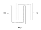
- Figure 3 is a top view of the comb-shaped electrode 203 in the liquid crystal display device according to the present invention.
- Figure 4 is a sectional view of the liquid crystal molecules distribution in the reflective display mode wherein voltages are applied to the opaque first comb-shaped electrode 301 and the transparent ITO electrode 205 of the upper substrate in the liquid crystal display device according to the present invention.
- Figure 5 is a sectional view of the electrode structure of the lower substrate and the liquid crystal distribution in the liquid crystal display device according to the present invention when no voltage is applied.
- Figure 6 is a distribution view of the liquid crystal molecules and the electric field lines in the liquid crystal display device according to the present invention when different voltages are applied to the first comb-shaped electrode 301 and the second comb-shaped electrode 302.
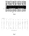
- Figure 7 is an electro-optic graph when the liquid crystal display device according to the present invention is operated in the reflective display mode shown in Fig.4 .
- Figures 8a-8c are electro-optic graphs when the liquid crystal display device according to the present invention is operated in the transmission display mode shown in Fig.6 wherein different voltages are applied to the first comb-shaped electrode 301 and the second comb-shaped electrode 302.
- FIG. 2 shows a structure diagram of a liquid crystal display device according to the present invention.
- the liquid crystal display device in Fig.2 includes an upper substrate 202, a transparent ITO electrode 205 disposed on a surface of the upper substrate 202 facing the liquid crystal layer, a color filter (not shown in Fig.2 ) disposed on the upper substrate 202, a lower substrate 201 parallel to the upper substrate 202, a comb-shaped electrode 203 disposed on a surface of the lower substrate 201 facing the liquid crystal layer, scanning lines and data lines (not shown in Fig 2 ) disposed on the lower substrate 201, a liquid crystal layer 206 with positive Dielectric Constant sandwiched between the upper substrate and the lower substrate, wherein the molecules of liquid crystal layer 206 is arranged parallel to the upper substrate when no voltage is applied, and a backlight unit 204 disposed adjacent a surface of the lower substrate opposite to the liquid crystal layer.
- Fig.3 is a top view of the comb-shaped electrode 203.
- the comb-shaped electrode 203 includes a first comb-shaped electrode 301 and a second comb-shaped electrode 302 which are interdigitated, both the first comb-shaped electrode 301 and the second comb-shaped electrode 302 are reflective electrodes, or one of the first comb-shaped electrode and the second comb-shaped electrode of the lower substrate is a reflective electrode, and the other is a transparent electrode.
- the transparent electrode may be an ITO electrode, an IZO electrode, or an IGO electrode, or a combination thereof.
- the invention will be described by taking both the first comb-shaped electrode 301 and the second comb-shaped electrode 302 as reflective electrodes.
- Figure 4 is a sectional view of the liquid crystal display device according to the present invention.
- Figure 4 shows the distribution of liquid crystal molecules when the liquid crystal display device is operated in the reflective display mode wherein voltages are applied to the opaque first comb-shaped electrode 301 and the transparent ITO electrode 205. Referring to Figs.
- the second comb-shaped electrode 302 (or the first comb-shaped electrode 301) is floated, the comb-shaped electrode 203 is used as a reflective layer, and different voltages are applied to the first comb-shaped electrode 301 and the transparent ITO electrode 205 on the upper substrate to generate an electric field perpendicular to the upper substrate 202 between the first comb-shaped electrode 301 and the transparent ITO electrode 205 by which the liquid crystal molecules rotate in a plane perpendicular to the substrate 202, so that an reflective display mode with excellent displaying effect may be achieved by the liquid crystal device when the ambient light is strong.
- Figure 5 is a sectional view of the electrode structure of the lower substrate and the liquid crystal distribution in the liquid crystal display device according to the present invention when no voltage is applied.
- Figure 6 is a distribution view of the liquid crystal molecules and the electric field lines in the liquid crystal display device according to the present invention when different voltages are applied to the first comb-shaped electrode 301 and the second comb-shaped electrode 302.
- the transparent ITO electrode on the upper substrate (not shown in the Figures) is floated, different voltages are applied to the first comb-shaped electrode 301 and the second comb-shaped electrode 302 to generate a electric field parallel to the upper substrate 202 between the first comb-shaped electrode 301 and the second comb-shaped electrode 302 by which the liquid crystal molecules rotate in a plane parallel to the upper substrate 202, so that an transmission display mode with excellent displaying effect and wide viewing angle may be achieved by the liquid crystal device when the ambient light is weak.
- Figure 7 is an electro-optic graph of the liquid crystal display device when the liquid crystal display device according to the present invention is operated in the reflective display mode shown in Fig.4 .
- Figures 8a-8c are electro-optic graphs of the liquid crystal display device when the liquid crystal display device of the present invention is operated in the transmission display mode shown in Fig.6 wherein different voltages are applied between the first comb-shaped electrode 301 and the second comb-shaped electrode 302.
- Figure 8a is an electro-optic graph of the liquid crystal display device and an arrangement view of liquid crystal molecules in the case of the transmission display mode when no voltage is applied.
- Figure 8b is an electro-optic graph and an arrangement view of liquid crystal molecules in the case of the transmission display mode when a moderate voltage is applied.
- Figure 8c is an electro-optic graph and an arrangement view of liquid crystal molecules in the case of the transmission display mode when a strongest voltage of 5V is applied.
- two polarizers are disposed on the upper side and the lower side of the liquid crystal cell , respectively , so that the absorbing axes thereof are at an angle of 45 degree with respect to long axis of the liquid crystal molecules, and absorbing axes of the two polarization planes (not shown in figures) are orthogonal to each other.
- the liquid crystal display device of the present invention when the liquid crystal display device of the present invention is operated in the transmission display mode, the biggest voltage difference between the first comb-shaped electrode 301 and the second comb-shaped electrode 302 on the lower substrate is 5V, and the electro-optic graph is a graph in a normally white display mode.
- the electro-optic graph is also a graph in a normally white display mode. Therefore, a transreflective liquid crystal display device with excellent display effect can be implemented wherein the transmission display mode and the reflective display mode are both normally white display mode, so long as the range of voltage is properly selected.
- a transreflective liquid crystal display with excellent display effect under various intensities of various ambient lights can be implemented by selecting different display modes, and it is unnecessary to have a dual cell gap or to have two TFTs disposed in the transmission region and the reflective region of a single pixel, respectively.Thus the process of manufacturing the liquid crystal display will be simplified and the cost will be reduced. Furthermore, the process may be simplified due to a more simple structure of the transreflective liquid crystal display, and a high yield rate of the transreflective liquid crystal display is achieved.
Landscapes
- Physics & Mathematics (AREA)
- Nonlinear Science (AREA)
- Mathematical Physics (AREA)
- Chemical & Material Sciences (AREA)
- Crystallography & Structural Chemistry (AREA)
- General Physics & Mathematics (AREA)
- Optics & Photonics (AREA)
- Geometry (AREA)
- Liquid Crystal (AREA)
- Liquid Crystal Display Device Control (AREA)
Applications Claiming Priority (2)
| Application Number | Priority Date | Filing Date | Title |
|---|---|---|---|
| CN2008100341941A CN101526703B (zh) | 2008-03-04 | 2008-03-04 | 透射反射液晶显示装置 |
| PCT/CN2009/070541 WO2009109122A1 (zh) | 2008-03-04 | 2009-02-26 | 透射反射液晶显示装置 |
Publications (3)
| Publication Number | Publication Date |
|---|---|
| EP2249196A1 true EP2249196A1 (de) | 2010-11-10 |
| EP2249196A4 EP2249196A4 (de) | 2011-04-27 |
| EP2249196B1 EP2249196B1 (de) | 2017-11-15 |
Family
ID=41055548
Family Applications (1)
| Application Number | Title | Priority Date | Filing Date |
|---|---|---|---|
| EP09717315.7A Not-in-force EP2249196B1 (de) | 2008-03-04 | 2009-02-26 | Transflektive flüssigkristallanzeigeeinrichtung |
Country Status (5)
| Country | Link |
|---|---|
| US (1) | US8400386B2 (de) |
| EP (1) | EP2249196B1 (de) |
| KR (1) | KR101275934B1 (de) |
| CN (1) | CN101526703B (de) |
| WO (1) | WO2009109122A1 (de) |
Cited By (1)
| Publication number | Priority date | Publication date | Assignee | Title |
|---|---|---|---|---|
| CN104036752A (zh) * | 2013-03-08 | 2014-09-10 | 联想(北京)有限公司 | 一种信息处理的方法及电子设备 |
Families Citing this family (2)
| Publication number | Priority date | Publication date | Assignee | Title |
|---|---|---|---|---|
| CN102645796B (zh) * | 2011-02-22 | 2015-04-29 | 上海天马微电子有限公司 | 一种液晶显示装置 |
| CN112987419B (zh) * | 2021-04-13 | 2023-09-15 | 成都天马微电子有限公司 | 一种显示装置及其制造方法 |
Family Cites Families (28)
| Publication number | Priority date | Publication date | Assignee | Title |
|---|---|---|---|---|
| JP3465835B2 (ja) | 1995-08-21 | 2003-11-10 | 松下電器産業株式会社 | アクティブマトリクス型液晶表示装置 |
| CN1176396C (zh) * | 2001-11-01 | 2004-11-17 | 瀚宇彩晶股份有限公司 | 同平面切换模式液晶显示单元的制造方法 |
| JP4117148B2 (ja) * | 2002-05-24 | 2008-07-16 | 日本電気株式会社 | 半透過型液晶表示装置 |
| US7006061B2 (en) * | 2002-06-04 | 2006-02-28 | Ngk Insulators, Ltd. | Display device |
| JP4082683B2 (ja) * | 2003-09-29 | 2008-04-30 | 株式会社 日立ディスプレイズ | 半透過型液晶表示装置 |
| TW200525214A (en) * | 2004-01-16 | 2005-08-01 | Innolux Display Corp | Liquid crystal display device |
| US7468719B2 (en) * | 2004-02-09 | 2008-12-23 | Advanced Lcd Technologies Development Center Co., Ltd. | Liquid crystal pixel memory, liquid crystal display, and methods of driving the same |
| JP4367206B2 (ja) | 2004-04-01 | 2009-11-18 | セイコーエプソン株式会社 | 視角制御素子、液晶表示装置、電子機器 |
| JP2005292709A (ja) * | 2004-04-05 | 2005-10-20 | Toshiba Matsushita Display Technology Co Ltd | 液晶表示素子 |
| JP4143569B2 (ja) * | 2004-05-14 | 2008-09-03 | キヤノン株式会社 | カラー表示装置 |
| JP2006126551A (ja) * | 2004-10-29 | 2006-05-18 | Hitachi Displays Ltd | 液晶表示装置 |
| JP3939723B2 (ja) * | 2004-11-05 | 2007-07-04 | 統寶光電股▲ふん▼有限公司 | 半透過型液晶ディスプレイ |
| US7239365B2 (en) * | 2004-11-09 | 2007-07-03 | Tpo Displays Corp. | Transflective liquid crystal display |
| US7652811B2 (en) * | 2005-03-07 | 2010-01-26 | Mark W Miles | Small mechanical optical shutter with non-imaging concentrating optics |
| KR101189268B1 (ko) * | 2005-03-08 | 2012-10-09 | 삼성디스플레이 주식회사 | 액정 표시 장치용 박막 표시판 및 구동 장치와 이를 포함하는 액정 표시 장치 |
| US7339641B2 (en) * | 2005-04-20 | 2008-03-04 | Research Foundation Of The University Of Central Florida | Transflective liquid crystal display with fringing and longitudinal electric field |
| JP4813842B2 (ja) * | 2005-07-29 | 2011-11-09 | 株式会社 日立ディスプレイズ | 液晶表示装置 |
| KR101244547B1 (ko) | 2005-09-16 | 2013-03-18 | 엘지디스플레이 주식회사 | 횡전계방식 액정표시장치, 그 제조 방법 및 액정패널의구동방법 |
| US8233124B2 (en) * | 2005-12-28 | 2012-07-31 | Lg Display Co., Ltd. | Liquid crystal display device |
| US7667808B2 (en) * | 2005-12-28 | 2010-02-23 | Lg Display Co., Ltd. | Liquid crystal display device and method of driving the same |
| JP2007178907A (ja) * | 2005-12-28 | 2007-07-12 | Lg Philips Lcd Co Ltd | 液晶表示装置 |
| KR20070070721A (ko) | 2005-12-29 | 2007-07-04 | 엘지.필립스 엘시디 주식회사 | 액정표시장치 및 그 구동방법 |
| JP4927429B2 (ja) * | 2006-04-05 | 2012-05-09 | 株式会社 日立ディスプレイズ | 半透過型液晶表示装置 |
| US8208102B2 (en) * | 2006-07-21 | 2012-06-26 | Sharp Kabushiki Kaisha | Display device having reflective region and transmissive region |
| JP4337854B2 (ja) * | 2006-09-19 | 2009-09-30 | エプソンイメージングデバイス株式会社 | 液晶表示装置 |
| TW200815859A (en) * | 2006-09-19 | 2008-04-01 | Epson Imaging Devices Corp | Liquid crystal display device |
| JP5177999B2 (ja) * | 2006-12-05 | 2013-04-10 | 株式会社半導体エネルギー研究所 | 液晶表示装置 |
| JP2009237297A (ja) * | 2008-03-27 | 2009-10-15 | Toshiba Corp | 液晶表示装置及びその駆動方法 |
-
2008
- 2008-03-04 CN CN2008100341941A patent/CN101526703B/zh active Active
-
2009
- 2009-02-26 WO PCT/CN2009/070541 patent/WO2009109122A1/zh not_active Ceased
- 2009-02-26 KR KR1020107018212A patent/KR101275934B1/ko not_active Expired - Fee Related
- 2009-02-26 US US12/866,174 patent/US8400386B2/en not_active Expired - Fee Related
- 2009-02-26 EP EP09717315.7A patent/EP2249196B1/de not_active Not-in-force
Cited By (1)
| Publication number | Priority date | Publication date | Assignee | Title |
|---|---|---|---|---|
| CN104036752A (zh) * | 2013-03-08 | 2014-09-10 | 联想(北京)有限公司 | 一种信息处理的方法及电子设备 |
Also Published As
| Publication number | Publication date |
|---|---|
| EP2249196A4 (de) | 2011-04-27 |
| WO2009109122A1 (zh) | 2009-09-11 |
| KR101275934B1 (ko) | 2013-06-14 |
| EP2249196B1 (de) | 2017-11-15 |
| US8400386B2 (en) | 2013-03-19 |
| KR20100102722A (ko) | 2010-09-24 |
| CN101526703A (zh) | 2009-09-09 |
| CN101526703B (zh) | 2011-08-17 |
| US20100321368A1 (en) | 2010-12-23 |
Similar Documents
| Publication | Publication Date | Title |
|---|---|---|
| US7903080B2 (en) | Liquid crystal display including a liquid crystal panel having two screens | |
| US7609345B2 (en) | Substrate for liquid crystal display and liquid crystal display having the same | |
| JP6068052B2 (ja) | 液晶表示素子 | |
| WO2014119395A1 (ja) | 液晶表示装置 | |
| KR101174164B1 (ko) | 반사투과형 액정표시장치 | |
| JP2002098961A (ja) | 液晶装置及び電子機器 | |
| KR20050070714A (ko) | 강유전성 액정배향막을 구비한 반투과형 평면구동모드액정표시소자 | |
| KR101888516B1 (ko) | 듀얼 모드 액정표시장치 | |
| CN101276087A (zh) | 液晶显示装置 | |
| KR20050033624A (ko) | 반투과형 액정 디스플레이 디바이스 | |
| US20100110318A1 (en) | Liquid crystal display device | |
| KR20050060847A (ko) | 액정 표시 장치와, 이의 광학 필름 어셈블리 | |
| US8400386B2 (en) | Transflective liquid crystal display device | |
| CN110221499A (zh) | 低边缘场串扰的LCoS微显示器 | |
| KR101855985B1 (ko) | 비씨에스엔 모드 액정표시장치 | |
| KR20060034399A (ko) | 반투과형 액정 표시 장치 및 그 제조 방법 | |
| KR20030068323A (ko) | 반사-투과형 액정 표시 장치 | |
| KR20080083791A (ko) | 반투과형 액정표시장치 및 그 제조방법 | |
| US20050140902A1 (en) | In plane switching liquid crystal display with transflector | |
| US7633572B2 (en) | Liquid crystal display and method of driving the same | |
| US8212986B2 (en) | LCD device, display method thereof and electronic apparatus employing LCD device | |
| US11977308B2 (en) | Liquid crystal display device and portable device | |
| JPH1138410A (ja) | 液晶表示装置 | |
| KR100765434B1 (ko) | 반투과형 디스플레이 장치 | |
| KR101688593B1 (ko) | 횡전계 모드 반사투과형 액정표시장치 |
Legal Events
| Date | Code | Title | Description |
|---|---|---|---|
| PUAI | Public reference made under article 153(3) epc to a published international application that has entered the european phase |
Free format text: ORIGINAL CODE: 0009012 |
|
| 17P | Request for examination filed |
Effective date: 20100805 |
|
| AK | Designated contracting states |
Kind code of ref document: A1 Designated state(s): AT BE BG CH CY CZ DE DK EE ES FI FR GB GR HR HU IE IS IT LI LT LU LV MC MK MT NL NO PL PT RO SE SI SK TR |
|
| AX | Request for extension of the european patent |
Extension state: AL BA RS |
|
| A4 | Supplementary search report drawn up and despatched |
Effective date: 20110324 |
|
| DAX | Request for extension of the european patent (deleted) | ||
| 17Q | First examination report despatched |
Effective date: 20140918 |
|
| GRAP | Despatch of communication of intention to grant a patent |
Free format text: ORIGINAL CODE: EPIDOSNIGR1 |
|
| INTG | Intention to grant announced |
Effective date: 20170707 |
|
| GRAS | Grant fee paid |
Free format text: ORIGINAL CODE: EPIDOSNIGR3 |
|
| GRAA | (expected) grant |
Free format text: ORIGINAL CODE: 0009210 |
|
| AK | Designated contracting states |
Kind code of ref document: B1 Designated state(s): AT BE BG CH CY CZ DE DK EE ES FI FR GB GR HR HU IE IS IT LI LT LU LV MC MK MT NL NO PL PT RO SE SI SK TR |
|
| REG | Reference to a national code |
Ref country code: CH Ref legal event code: EP Ref country code: GB Ref legal event code: FG4D Ref country code: AT Ref legal event code: REF Ref document number: 946844 Country of ref document: AT Kind code of ref document: T Effective date: 20171115 |
|
| REG | Reference to a national code |
Ref country code: IE Ref legal event code: FG4D |
|
| REG | Reference to a national code |
Ref country code: DE Ref legal event code: R096 Ref document number: 602009049360 Country of ref document: DE |
|
| REG | Reference to a national code |
Ref country code: NL Ref legal event code: MP Effective date: 20171115 |
|
| REG | Reference to a national code |
Ref country code: LT Ref legal event code: MG4D |
|
| REG | Reference to a national code |
Ref country code: AT Ref legal event code: MK05 Ref document number: 946844 Country of ref document: AT Kind code of ref document: T Effective date: 20171115 |
|
| PG25 | Lapsed in a contracting state [announced via postgrant information from national office to epo] |
Ref country code: LT Free format text: LAPSE BECAUSE OF FAILURE TO SUBMIT A TRANSLATION OF THE DESCRIPTION OR TO PAY THE FEE WITHIN THE PRESCRIBED TIME-LIMIT Effective date: 20171115 Ref country code: NL Free format text: LAPSE BECAUSE OF FAILURE TO SUBMIT A TRANSLATION OF THE DESCRIPTION OR TO PAY THE FEE WITHIN THE PRESCRIBED TIME-LIMIT Effective date: 20171115 Ref country code: NO Free format text: LAPSE BECAUSE OF FAILURE TO SUBMIT A TRANSLATION OF THE DESCRIPTION OR TO PAY THE FEE WITHIN THE PRESCRIBED TIME-LIMIT Effective date: 20180215 Ref country code: FI Free format text: LAPSE BECAUSE OF FAILURE TO SUBMIT A TRANSLATION OF THE DESCRIPTION OR TO PAY THE FEE WITHIN THE PRESCRIBED TIME-LIMIT Effective date: 20171115 Ref country code: ES Free format text: LAPSE BECAUSE OF FAILURE TO SUBMIT A TRANSLATION OF THE DESCRIPTION OR TO PAY THE FEE WITHIN THE PRESCRIBED TIME-LIMIT Effective date: 20171115 Ref country code: SE Free format text: LAPSE BECAUSE OF FAILURE TO SUBMIT A TRANSLATION OF THE DESCRIPTION OR TO PAY THE FEE WITHIN THE PRESCRIBED TIME-LIMIT Effective date: 20171115 |
|
| PG25 | Lapsed in a contracting state [announced via postgrant information from national office to epo] |
Ref country code: BG Free format text: LAPSE BECAUSE OF FAILURE TO SUBMIT A TRANSLATION OF THE DESCRIPTION OR TO PAY THE FEE WITHIN THE PRESCRIBED TIME-LIMIT Effective date: 20180215 Ref country code: LV Free format text: LAPSE BECAUSE OF FAILURE TO SUBMIT A TRANSLATION OF THE DESCRIPTION OR TO PAY THE FEE WITHIN THE PRESCRIBED TIME-LIMIT Effective date: 20171115 Ref country code: HR Free format text: LAPSE BECAUSE OF FAILURE TO SUBMIT A TRANSLATION OF THE DESCRIPTION OR TO PAY THE FEE WITHIN THE PRESCRIBED TIME-LIMIT Effective date: 20171115 Ref country code: GR Free format text: LAPSE BECAUSE OF FAILURE TO SUBMIT A TRANSLATION OF THE DESCRIPTION OR TO PAY THE FEE WITHIN THE PRESCRIBED TIME-LIMIT Effective date: 20180216 Ref country code: AT Free format text: LAPSE BECAUSE OF FAILURE TO SUBMIT A TRANSLATION OF THE DESCRIPTION OR TO PAY THE FEE WITHIN THE PRESCRIBED TIME-LIMIT Effective date: 20171115 |
|
| PG25 | Lapsed in a contracting state [announced via postgrant information from national office to epo] |
Ref country code: CZ Free format text: LAPSE BECAUSE OF FAILURE TO SUBMIT A TRANSLATION OF THE DESCRIPTION OR TO PAY THE FEE WITHIN THE PRESCRIBED TIME-LIMIT Effective date: 20171115 Ref country code: EE Free format text: LAPSE BECAUSE OF FAILURE TO SUBMIT A TRANSLATION OF THE DESCRIPTION OR TO PAY THE FEE WITHIN THE PRESCRIBED TIME-LIMIT Effective date: 20171115 Ref country code: CY Free format text: LAPSE BECAUSE OF FAILURE TO SUBMIT A TRANSLATION OF THE DESCRIPTION OR TO PAY THE FEE WITHIN THE PRESCRIBED TIME-LIMIT Effective date: 20171115 Ref country code: DK Free format text: LAPSE BECAUSE OF FAILURE TO SUBMIT A TRANSLATION OF THE DESCRIPTION OR TO PAY THE FEE WITHIN THE PRESCRIBED TIME-LIMIT Effective date: 20171115 Ref country code: SK Free format text: LAPSE BECAUSE OF FAILURE TO SUBMIT A TRANSLATION OF THE DESCRIPTION OR TO PAY THE FEE WITHIN THE PRESCRIBED TIME-LIMIT Effective date: 20171115 |
|
| REG | Reference to a national code |
Ref country code: DE Ref legal event code: R097 Ref document number: 602009049360 Country of ref document: DE |
|
| PG25 | Lapsed in a contracting state [announced via postgrant information from national office to epo] |
Ref country code: IT Free format text: LAPSE BECAUSE OF FAILURE TO SUBMIT A TRANSLATION OF THE DESCRIPTION OR TO PAY THE FEE WITHIN THE PRESCRIBED TIME-LIMIT Effective date: 20171115 Ref country code: RO Free format text: LAPSE BECAUSE OF FAILURE TO SUBMIT A TRANSLATION OF THE DESCRIPTION OR TO PAY THE FEE WITHIN THE PRESCRIBED TIME-LIMIT Effective date: 20171115 Ref country code: PL Free format text: LAPSE BECAUSE OF FAILURE TO SUBMIT A TRANSLATION OF THE DESCRIPTION OR TO PAY THE FEE WITHIN THE PRESCRIBED TIME-LIMIT Effective date: 20171115 |
|
| REG | Reference to a national code |
Ref country code: CH Ref legal event code: PL |
|
| PLBE | No opposition filed within time limit |
Free format text: ORIGINAL CODE: 0009261 |
|
| STAA | Information on the status of an ep patent application or granted ep patent |
Free format text: STATUS: NO OPPOSITION FILED WITHIN TIME LIMIT |
|
| PG25 | Lapsed in a contracting state [announced via postgrant information from national office to epo] |
Ref country code: MC Free format text: LAPSE BECAUSE OF FAILURE TO SUBMIT A TRANSLATION OF THE DESCRIPTION OR TO PAY THE FEE WITHIN THE PRESCRIBED TIME-LIMIT Effective date: 20171115 |
|
| 26N | No opposition filed |
Effective date: 20180817 |
|
| GBPC | Gb: european patent ceased through non-payment of renewal fee |
Effective date: 20180226 |
|
| REG | Reference to a national code |
Ref country code: IE Ref legal event code: MM4A |
|
| REG | Reference to a national code |
Ref country code: BE Ref legal event code: MM Effective date: 20180228 |
|
| PG25 | Lapsed in a contracting state [announced via postgrant information from national office to epo] |
Ref country code: CH Free format text: LAPSE BECAUSE OF NON-PAYMENT OF DUE FEES Effective date: 20180228 Ref country code: LI Free format text: LAPSE BECAUSE OF NON-PAYMENT OF DUE FEES Effective date: 20180228 Ref country code: LU Free format text: LAPSE BECAUSE OF NON-PAYMENT OF DUE FEES Effective date: 20180226 Ref country code: SI Free format text: LAPSE BECAUSE OF FAILURE TO SUBMIT A TRANSLATION OF THE DESCRIPTION OR TO PAY THE FEE WITHIN THE PRESCRIBED TIME-LIMIT Effective date: 20171115 |
|
| REG | Reference to a national code |
Ref country code: FR Ref legal event code: ST Effective date: 20181031 |
|
| PG25 | Lapsed in a contracting state [announced via postgrant information from national office to epo] |
Ref country code: IE Free format text: LAPSE BECAUSE OF NON-PAYMENT OF DUE FEES Effective date: 20180226 |
|
| PG25 | Lapsed in a contracting state [announced via postgrant information from national office to epo] |
Ref country code: GB Free format text: LAPSE BECAUSE OF NON-PAYMENT OF DUE FEES Effective date: 20180226 Ref country code: FR Free format text: LAPSE BECAUSE OF NON-PAYMENT OF DUE FEES Effective date: 20180228 Ref country code: BE Free format text: LAPSE BECAUSE OF NON-PAYMENT OF DUE FEES Effective date: 20180228 |
|
| PG25 | Lapsed in a contracting state [announced via postgrant information from national office to epo] |
Ref country code: MT Free format text: LAPSE BECAUSE OF NON-PAYMENT OF DUE FEES Effective date: 20180226 |
|
| PG25 | Lapsed in a contracting state [announced via postgrant information from national office to epo] |
Ref country code: TR Free format text: LAPSE BECAUSE OF FAILURE TO SUBMIT A TRANSLATION OF THE DESCRIPTION OR TO PAY THE FEE WITHIN THE PRESCRIBED TIME-LIMIT Effective date: 20171115 |
|
| PG25 | Lapsed in a contracting state [announced via postgrant information from national office to epo] |
Ref country code: HU Free format text: LAPSE BECAUSE OF FAILURE TO SUBMIT A TRANSLATION OF THE DESCRIPTION OR TO PAY THE FEE WITHIN THE PRESCRIBED TIME-LIMIT; INVALID AB INITIO Effective date: 20090226 Ref country code: PT Free format text: LAPSE BECAUSE OF FAILURE TO SUBMIT A TRANSLATION OF THE DESCRIPTION OR TO PAY THE FEE WITHIN THE PRESCRIBED TIME-LIMIT Effective date: 20171115 |
|
| PG25 | Lapsed in a contracting state [announced via postgrant information from national office to epo] |
Ref country code: MK Free format text: LAPSE BECAUSE OF NON-PAYMENT OF DUE FEES Effective date: 20171115 |
|
| PG25 | Lapsed in a contracting state [announced via postgrant information from national office to epo] |
Ref country code: IS Free format text: LAPSE BECAUSE OF FAILURE TO SUBMIT A TRANSLATION OF THE DESCRIPTION OR TO PAY THE FEE WITHIN THE PRESCRIBED TIME-LIMIT Effective date: 20180315 |
|
| PGFP | Annual fee paid to national office [announced via postgrant information from national office to epo] |
Ref country code: DE Payment date: 20230216 Year of fee payment: 15 |
|
| REG | Reference to a national code |
Ref country code: DE Ref legal event code: R119 Ref document number: 602009049360 Country of ref document: DE |
|
| PG25 | Lapsed in a contracting state [announced via postgrant information from national office to epo] |
Ref country code: DE Free format text: LAPSE BECAUSE OF NON-PAYMENT OF DUE FEES Effective date: 20240903 |
|
| PG25 | Lapsed in a contracting state [announced via postgrant information from national office to epo] |
Ref country code: DE Free format text: LAPSE BECAUSE OF NON-PAYMENT OF DUE FEES Effective date: 20240903 |