EP2249227B1 - Dispositif d'interface pour dispositif hôte, dispositif d'interface pour dispositif esclave, dispositif hôte, dispositif esclave, système de communication et procédé de commutation de tension d'interface - Google Patents
Dispositif d'interface pour dispositif hôte, dispositif d'interface pour dispositif esclave, dispositif hôte, dispositif esclave, système de communication et procédé de commutation de tension d'interface Download PDFInfo
- Publication number
- EP2249227B1 EP2249227B1 EP09713710.3A EP09713710A EP2249227B1 EP 2249227 B1 EP2249227 B1 EP 2249227B1 EP 09713710 A EP09713710 A EP 09713710A EP 2249227 B1 EP2249227 B1 EP 2249227B1
- Authority
- EP
- European Patent Office
- Prior art keywords
- interface voltage
- interface
- host device
- slave device
- input
- Prior art date
- Legal status (The legal status is an assumption and is not a legal conclusion. Google has not performed a legal analysis and makes no representation as to the accuracy of the status listed.)
- Active
Links
Images



Classifications
-
- G—PHYSICS
- G06—COMPUTING OR CALCULATING; COUNTING
- G06F—ELECTRIC DIGITAL DATA PROCESSING
- G06F1/00—Details not covered by groups G06F3/00 - G06F13/00 and G06F21/00
- G06F1/26—Power supply means, e.g. regulation thereof
Definitions
- the present invention relates to an interface circuit (device) that switches an interface voltage in a stable and efficient manner during operation of a host device and a slave device in a communication system in which an operating voltage can be selected from a plurality of interface voltages, a host device, a slave device, and a communication system including the interface circuit, and an interface voltage switching method.
- slave devices that have penetrated the market use large-capacity nonvolatile storage elements, such as flash memories, and process data at a high speed.
- Examples of such slave devices include secure digital (SD) cards and memory sticks.
- SD secure digital
- the slave devices are used in, for example, personal computers, personal digital assistants (PDAs), mobile telephones, digital cameras, audio players, and car navigation systems, which function as host devices that can use the slave devices.
- PDAs personal digital assistants
- mobile telephones digital cameras
- audio players audio players
- car navigation systems which function as host devices that can use the slave devices.
- the slave devices that have been commercialized recently can also have, for example, wireless LAN functions, network connection functions for wireless communication based on Bluetooth (trademark), positioning functions using the global positioning system (GPS), and input and output functions such as one-segment broadcasting reception functions for terrestrial digital TV broadcasting. Host devices are connected to these slave device to use the functions of the slave devices.
- wireless LAN functions for example, wireless LAN functions, network connection functions for wireless communication based on Bluetooth (trademark), positioning functions using the global positioning system (GPS), and input and output functions such as one-segment broadcasting reception functions for terrestrial digital TV broadcasting.
- GPS global positioning system
- input and output functions such as one-segment broadcasting reception functions for terrestrial digital TV broadcasting.
- Host devices are connected to these slave device to use the functions of the slave devices.
- a communication system that includes such a host device and such a slave device tends to process an increasingly larger amount of data every year. This has generated a market demand for increasing the processing speed of an interface between the host device and the slave device. There also is a market demand for maintaining compatibility with the existing interfaces that are widely used in the market so that the existing interfaces will be usable continuously.
- an interface voltage (voltage used in the interface device) needs to be lowered.
- the host device and the slave device may have a determination key indicating the level of an interface voltage, and the host device may detect an interface voltage of the slave device and then switch the voltage to be supplied to the slave voltage to determine the interface voltage (see, for example, Patent Citation 1).
- Patent Citation 1 Japanese Unexamined Patent Publication No. 2002-169631
- the above conventional technique requires the interface device to have a dedicated terminal for every different interface voltage to determine the interface voltage, and therefore cannot be applied to the existing interface specifications having only a fixed number of interface terminals.
- the host device determines the interface voltage by detecting a determination key that has been provided from the slave device. In this case, the host device cannot determine whether switching of the interface voltage has been completed successfully in the slave device when the interface voltage is to be switched during operation (while, for example, the host device and the slave device can transmit and receive data to and from each other). This degrades the reliability of the communication system.
- the conventional technique assumes that the interface voltage used between the host device and the slave device has the same level as the voltage supplied from the host device to the slave device. With such technique, it is impossible to switch only the voltage of the interface circuit in a stable manner during operation without changing the operating voltage of the slave device.
- an object of the present invention to provide an interface circuit (interface device) that executes switching control of only an interface voltage used between a host device and a slave device in a more reliable manner than conventional techniques while requiring the same number of signal lines as the existing interface specifications, a host device, a slave device, and a communication system including the interface circuit (interface device), and an interface voltage switching method.
- a first aspect of the present invention provides an interface device, used in a host device connected to a slave device to transmit and receive data and/or a command to and from the slave device, that switches an interface voltage used for communication between the slave device and the host device.
- the interface device includes a clock output unit, a terminal group, and an interface voltage switching unit.
- the clock output unit outputs a clock signal for transmitting and receiving the data and/or the command.
- the terminal group includes one or more input/output terminal units that transmits and receives the data and/or the command using one of a first interface voltage and a second interface voltage.
- the interface voltage switching unit selects one of the first interface voltage and the second interface voltage and switches the interface voltage used for communication between the host device and the slave device to the selected one of the first and second interface voltages.
- the interface voltage switching unit includes a control unit, a clock control unit, and an input/output terminal control unit.
- the clock control unit is controlled by the control unit, and fixes a level of a signal output from the clock output unit to a first signal level when the interface voltage used for communication between the host device and the slave device is to be switched, and, when an interface voltage in the host device has been switched to the selected interface voltage, controls the clock output unit to output a clock signal using the selected interface voltage.
- the input/output terminal control unit is controlled by the control unit, and sets the one or more input/output terminal units to an input state, and monitors a level of an input signal into the one or more input/output terminal units when the interface voltage used for communication between the host device and the slave device is to be switched, and transmits, when detecting that the level of the input signal into the one or more input/output terminal units becomes a signal level indicating that an interface voltage in the slave device has been switched to the selected interface voltage, transmits a notification indicating the detection result to the control unit.
- the control unit determines that the interface voltage in the slave device has been switched when receiving the notification indicating that the interface voltage switching has been completed in the slave device transmitted from the input/output terminal control unit after the clock control unit is set to a state in which the clock signal is being outputted using the selected interface voltage.
- This structure enables a host device and a slave device using this interface device for a host device to switch an interface voltage with a simple method while maintaining the signal level of buses (communication paths between the host device and the slave device connected using the terminal group) in a stable manner, and enables the interface voltage switching control to be executed in a more reliable manner than with conventional techniques.
- this structure enables an interface voltage to be switched in a stable and efficient manner during operation of a host device and a slave device in a communication system in which an operating voltage can be selected from a plurality of interface voltages while requiring the same number of buses as the existing interface specifications having at least two signal lines.
- the interface device may be an interface circuit.
- a second aspect of the present invention provides the interface device of the first aspect of the present invention in which the first signal level is a low level.
- a third aspect of the present invention provides the interface device of the first or second aspect of the present invention in which the control unit sets all the input/output terminal units to an input state when the interface voltage used for communication between the host device and the slave device is to be switched.
- a fourth aspect of the present invention provides the interface device of one of the first to third aspects of the present invention in which the control unit determines that the interface voltage in the host device and the interface voltage in the slave device have been switched when the level of the input signal into the input/output terminal units becomes a high level at the selected interface voltage.
- a fifth aspect of the present invention provides an interface device used in a host device connected to a slave device to transmit and receive data and/or a command to and from the slave device, that switches an interface voltage used for communication between the slave device and the host device.
- the interface device includes a clock output unit, a terminal group, and an interface voltage switching unit.
- the clock output unit outputs a clock signal for transmitting and receiving the data and/or the command.
- the terminal group includes one or more input/output terminal units that transmits and receives the data and/or the command using one of a first interface voltage and a second interface voltage.
- the interface voltage switching unit selects one of the first interface voltage and the second interface voltage and switches the interface voltage used for communication between the host device and the slave device to the selected one of the first and second interface voltages.
- the interface voltage switching unit includes a control unit, a clock control unit, and an input/output terminal control unit.
- the clock control unit is controlled by the control unit, and controls the clock output unit to output a signal having a first signal level when the interface voltage used for communication between the host device and the slave device is to be switched, and, when an interface voltage in the host device has been switched to the selected interface voltage, controls , the clock output unit to output a clock signal using the selected interface voltage.
- the input/output terminal control unit is controlled by the control unit, and sets the one or more input/output terminal units to an output state at the first signal level when the interface voltage used for communication between the host device and the slave device is to be switched, and, when the interface voltage in the host device has been switched to the selected interface voltage, switches the one or more input/output terminal units from the output state at the first signal level to an input state and monitors a level of an input signal into the one or more input/output terminal units, and transmits, when detecting that the level of the input signal into the one or more input/output terminal units becomes a signal level indicating that an interface voltage in the slave device has been switched to the selected voltage, a notification indicating the detection result to the control unit.
- the control unit determines that the interface voltage in the slave device has been switched when receiving the notification indicating that the interface voltage switching has been completed in the slave device from the input/output terminal control unit after the clock control unit is set to a state in which a clock signal is being outputted using the selected interface voltage.
- This structure enables a host device and a slave device using this interface device for a host device to switch an interface voltage with a simple method while maintaining the signal level of buses (communication paths between the host device and the slave device connected using the terminal group) in a stable manner, and enables the interface voltage switching control to be executed in a more reliable manner than with conventional techniques.
- this structure enables an interface voltage to be switched in a stable and efficient manner during operation of a host device and a slave device in a communication system in which an operating voltage can be selected from a plurality of interface voltages while requiring the same number of buses as the existing interface specifications having at least two signal lines.
- the interface device may be an interface circuit.
- a sixth aspect of the present invention provides the interface device of the fifth aspect of the present invention in which the control unit sets all the input/output terminal units to the output state at the first signal level when the interface voltage used for communication between the host device and the slave device is to be switched.
- a seventh aspect of the present invention provides the interface device of the fifth or sixth aspect of the present invention in which the interface voltage switching unit sets an input/output terminal unit for transmitting and receiving data to the output state at the first signal level when the interface voltage is to be switched.
- An eighth aspect of the present invention provides the interface device of one of the fifth to seventh aspects of the present invention in which the first signal level is a low level.
- a ninth aspect of the present invention provides the interface device of the eighth aspect of the present invention in which the interface voltage switching unit determines that the interface voltage in the host device and the interface voltage in the slave device have been switched when the level of the input signal into the input/output terminal units becomes a high level at the selected interface voltage.
- a tenth aspect of the present invention provides an interface device used in a slave device connected to a host device to transmit and receive data and/or a command to and from the host device, that switches an interface voltage used for communication between the slave device and the host device.
- the interface device includes a clock input unit, a terminal group, and an interface voltage switching unit.
- the clock input unit receives input of a clock signal for transmitting and receiving the data and/or the command.
- the terminal group includes one or more input/output terminal units that transmits and receives the data and/or the command using one of a first interface voltage and a second interface voltage.
- the interface voltage switching unit selects one of the first interface voltage and the second interface voltage and switches the interface voltage used for communication between the host device and the slave device to the selected one of the first and second interface voltages.
- the interface voltage switching unit includes a control unit and an input/output terminal control unit.
- the input/output terminal control unit is controlled by the control unit, and controls the one or more input/output terminal units to an output state at a first signal level when the interface voltage used for communication between the host device and the slave device is to be switched, and switches, when an interface voltage in the slave device has been switched to the selected interface voltage, the one or more input/output terminal units from the output state at the first signal level to an input state.
- An eleventh aspect of the present invention provides the interface device of the tenth aspect of the present invention in which the input/output terminal control unit controls all the input/output terminal units to the output state at the first signal level when the interface voltage used for communication between the host device and the slave device is to be switched.
- a twelfth aspect of the present invention provides the interface device of the tenth or eleventh aspect of the present invention in which the interface voltage switching unit determines that an interface voltage in the host device has been switched to the selected interface voltage through switching the input/output terminal units from the output state at the first signal level to the input state in synchronization with the clock signal inputted into the clock input unit.
- a thirteenth aspect of the present invention provides the interface device of one of the tenth to twelfth aspects of the present invention in which the interface voltage switching unit determines that the interface voltage in the host device has been switched to the selected interface voltage when a signal indicating completion of the switching is inputted into the input/output terminal units after switching the input/output terminal units from the output state at the first signal level to the input state in synchronization with the clock signal inputted into the clock input unit.
- a fourteenth aspect of the present invention provides the interface device of the tenth or eleventh aspect of the present invention in which the interface voltage switching unit switches the input/output terminal units from the output state at the first signal level to the input state in synchronization with the clock signal inputted into the clock input unit when the interface voltage has been switched.
- a fifteenth aspect of the present invention provides the interface device of one of the tenth, eleventh, and fourteenth aspects of the present invention in which the interface voltage switching unit switches at least one of the input/output terminal units that are in the output state at the first signal level to the input state when the interface voltage has been switched, and switches the remaining input/output terminal units that are in the output state at the first signal level to the input state in synchronization with the clock signal inputted into the clock input unit.
- a sixteenth aspect of the present invention provides the interface device of one of the tenth to fifteenth aspects of the present invention in which the input/output terminal control unit outputs a signal from the input/output terminal units as an open drain output.
- a seventeenth aspect of the present invention provides the interface device of one of the tenth to sixteenth aspects of the present invention in which when the interface voltage switching is terminated incompletely due to an error the interface voltage switching unit switches a command transmission/reception terminal unit, which is included in the terminal group and used to transmit and receive the data and/or the command, from the output state at the first signal level to the input state after a predetermined period elapses.
- An eighteenth aspect of the present invention provides the interface device of one of the tenth to seventeenth aspects of the present invention in which the first signal level is a low level.
- a nineteenth aspect of the present invention provides the interface device of the eighteenth aspect of the present invention in which the interface voltage switching unit determines that the interface voltage has been switched when the level of the input signal into the input/output terminal units becomes a high level.
- a twentieth aspect of the present invention provides a host device that includes the interface device of one of the first to ninth aspects of the present invention, and is connected to a slave device via the interface device to transmit and receive data and/or a command to and from the slave device.
- a twenty-first aspect of the present invention provides the host device of the twentieth aspect of the present invention that transmits, to the slave device, a command to obtain a time required for switching the interface voltage in the slave device before a process for switching the interface voltage used for communication between the slave device and the host device is performed.
- a twenty-second aspect of the present invention provides the host device of the twentieth or twenty-first aspect of the present invention that transmits, to the slave device, a command to determine whether the interface voltage has been switched successfully after a process for switching the interface voltage used for communication between the slave device and the host device is performed.
- a twenty-third aspect of the present invention provides a slave device that includes the interface device of one of the tenth to nineteenth aspects of the present invention and is connected to the host device via the interface device to transmit and receive data and/or a command to and from the host device.
- a twenty-fourth aspect of the present invention provides the slave device of the twenty-third aspect of the present invention in which a response to a command transmitted from the host device includes information about a maximum value of a time required for switching the interface voltage.
- a twenty-fifth aspect of the present invention provides the slave device of the twenty-third or twenty-fourth aspect of the present invention in which a response to a command transmitted from the host device includes status information indicating that the interface voltage has been switched successfully.
- a twenty-sixth aspect of the present invention provides a communication system including the host device of one of the twentieth to twenty-second aspects of the present invention and the slave device of one of the twenty-third to twenty-fifth aspects of the present invention.
- a twenty-seventh aspect of the present invention provides an interface voltage switching method for switching an interface voltage used for communication between a host device and a slave device.
- the method includes processes (1) to (7) below.
- the host device issues a command instructing to switch an interface voltage to the slave device.
- the slave device returns a response to the command instructing to switch the interface voltage to the host device.
- the host device stops providing a clock signal by fixing a level of a clock signal output to the slave device to a first signal level.
- the host device sets one or more input/output terminal units included in the host device to an input state.
- the slave device sets one or more input/output terminals included in the slave device to an output state at the first signal level.
- the slave device sets the input/output terminals of the slave device from the output state at the first signal level to the input state when an interface voltage has been switched in the slave device.
- the host device resumes to provide the clock signal when the interface voltage switching has been completed in the host device.
- the host device detects that a signal indicating completion of the interface voltage switching in the slave device has been input into the input/output terminals of the host device after the clock output is resumed, and determines that the interface voltage has been switched in the slave device.
- This method enables a host device and a slave device to switch an interface voltage with a simple method while maintaining the signal level of buses (communication paths between the host device and the slave device connected using the terminal group) in a stable manner, and enables the interface voltage switching control to be executed in a more reliable manner than with conventional techniques.
- this method enables an interface voltage to be switched in a stable and efficient manner during operation of a host device and a slave device in a communication system in which an operating voltage can be selected from a plurality of interface voltages while requiring the same number of buses as the existing interface specifications having at least two signal lines.
- the processes (1) to (7) in this method may be performed in an order different from the above order.
- a twenty-eighth aspect of the present invention provides an interface voltage switching method for switching an interface voltage used for communication between a host device and a slave device that communicate with each other from a first interface voltage V1 to a second interface voltage V2 via a first bus for transmitting a clock signal, a second bus for transmitting a command, and a third bus for transmitting data.
- the method includes processes (1) to (9) below.
- the host device issues a command CMD to the slave device to start an interface voltage switching sequence.
- the slave device returns a response to the command CMD to the host device.
- the slave device sets a signal level of the second bus and the third bus to a low level immediately after transmitting the response to the host device.
- the host device stops supplying the clock signal to the slave device, the slave device starts a process for switching the interface voltage after the host device stops providing the clock signal, the host device detects whether the interface voltage switching sequence is to be started by checking a signal level of one of the second bus and the third bus, and the host device 1 aborts the interface voltage switching sequence and executes power cycles when failing to detect a low level as the signal level of the one of the second bus and the third bus.
- the slave device stabilizes an interface voltage, to which the process for switching the interface voltage has been performed, outputted from a regulator included in the slave device within a predetermined period T1, and the host device fixes a level of the clock signal at a low level for at least the predetermined period T1.
- the host device 1 resumes to provide a clock signal at the second interface voltage V2 when a voltage output from a regulator included in the host device is stabilized after the predetermined period T1 elapses from the end of the process (4), and the slave device checks whether the level of the clock signal is a signal level that is based on the second interface voltage V2.
- the slave device 2 detects the clock signal and sets a signal level of the second bus to a high level using the second interface voltage V2 for at least a period of one clock cycle of the clock signal and then frees the second bus.
- the slave device checks whether the host device sets the signal level of the second bus to the second interface voltage V2 through a pull-up resistor R1 connected to the second bus of the host device.
- the slave device sets the signal level of the third bus to a high level for at least a period of one clock cycle and then frees the third bus when the process for switching the interface voltage has been completed successfully.
- the signal level of the third bus is set to a high level within a predetermined period T2 from when providing the clock signal is resumed.
- the host device checks whether the signal level of the third bus is a high level after the predetermined period T2 elapses from a timing t3 at which providing the clock is started.
- This method enables a host device and a slave device to switch an interface voltage with a simple method while maintaining the signal level of buses (communication paths between the host device and the slave device connected using the terminal group) in a stable manner, and enables the interface voltage switching control to be executed in a more reliable manner than with conventional techniques.
- this method enables an interface voltage to be switched in a stable and efficient manner during operation of a host device and a slave device in a communication system in which an operating voltage can be selected from a plurality of interface voltages while requiring the same number of buses as the existing interface specifications having at least two signal lines.
- the processes (1) to (9) in this method may be performed in an order different from the above order.
- a twenty-ninth aspect of the present invention provides an interface voltage switching method for switching an interface voltage used for communication between a host device and a slave device.
- the method includes processes (1) to (9) below.
- the host device transmits a command instructing to switch an interface voltage to the slave device.
- the slave device returns a response to the command instructing to switch the interface voltage to the host device.
- the host device stops providing a clock signal by fixing a level of a clock signal output to the slave device to a first signal level.
- the host device sets one or more input/output terminal units included in the host device to an output state at the first signal level.
- the slave device sets one or more input/output terminal units included in the slave device to the output state at the first signal level.
- the slave device sets the input/output terminals of the slave device from the output state at the first signal level to an input state when an interface voltage has been switched in the slave device.
- the host device resumes to provide the clock signal when the interface voltage has been switched in the host device.
- the host device sets the input/output terminals from the output state at the first signal level to an input state when the interface voltage has been switched in the host device.
- the host device detects that a signal indicating completion of the interface voltage switching in the slave device has been inputted into the input/output terminals of the host device after the clock output is resumed, and determines that the interface voltage switching has been completed in the slave device.
- This method enables a host device and a slave device to switch an interface voltage with a simple method while maintaining the signal level of buses (communication paths between the host device and the slave device connected using the terminal group) in a stable manner, and enables the interface voltage switching control to be executed in a more reliable manner than with conventional techniques.
- this method enables an interface voltage to be switched in a stable and efficient manner during operation of a host device and a slave device in a communication system in which an operating voltage can be selected from a plurality of interface voltages while requiring the same number of buses as the existing interface specifications having at least two signal lines.
- the processes (1) to (9) in this method may be performed in an order different from the above order.
- a thirtieth aspect of the present invention provides the interface voltage switching method of the twenty-seventh or twenty-ninth aspect of the present invention in which the first signal level is a low level.
- Part or all of the processes of the interface voltage switching method of one of the twenty-seventh to thirtieth aspects of the present invention may be implemented using a program that is executed by a computer.
- the interface circuit (the interface device (the interface device for a host device and the interface device for a slave device)) of the present invention, the host device, the slave device, and the communication system including the interface circuit (the interface device), and the interface voltage switching method enable an interface voltage to be switched while enabling a host device and a slave device to maintain the signal level of buses in a stable manner with a simple method, and enable the interface voltage switching control to be executed in a more reliable manner than with conventional techniques, and thus enable an interface voltage to be switched in a stable and efficient manner during operation of a host device and a slave device in a communication system in which an operating voltage can be selected from a plurality of interface voltages while requiring the same number of buses as the existing interface specifications having at least two signal lines.
- Fig. 1 shows the structure of a communication system according to a first embodiment of the present invention.
- the communication system includes a host device 1 and a slave device 2.
- the host device 1 and the slave device 2 are connected to each other with buses 30 to 32.
- the buses 31 and 32 are connected to an output voltage of a regulator, which will be described later, via pull-up resistors R1 and R2.
- the bus 30 is used to transmit clock signals.
- the bus 31 is used to transmit and receive commands.
- the bus 32 is used to transmit and receive data.
- the commands are transmitted from the host device 1 to the slave device 2 to, for example, write or read to or from a register, write or read to or from a memory area, or obtain the status of the slave device 2.
- the commands and the data are transmitted and received on the buses 31 and 32 basically in synchronization with the clock signals transmitted on the bus 30. However, when the buses 31 and 32 are used to transmit and receive asynchronous signals, such as signals associated with an interrupt, these signals may not be synchronized with the clocks transmitted on the bus 30.
- the host device 1 and the slave device 2 operate using a first interface voltage (described later) when the system is powered on.
- the structure of the host device 1 will be described first.
- the host device 1 includes an interface voltage switching unit 10, a terminal group 11, a regulator 12, and a voltage source 13.
- the other components of the host device 1 that are not essential to the present invention are not shown in the figure.
- the interface voltage switching unit 10 includes a controller 100, an input/output terminal control unit 101, a clock control unit 102, a detection circuit, and a stabilization waiting circuit.
- the controller 100 transmits a command to switch an interface voltage (interface voltage switching command) to the slave device 2, and also executes a series of control associated with an interface voltage switching process performed by the host device 1.
- the input/output terminal control unit 101 controls an input signal and an output signal that received/transmitted via input/output terminal units 111 and 112, which are included in the terminal group 11 (described later).
- the clock control unit 102 controls a signal to be outputted via a clock output terminal 110, which is included in the terminal group 11 (described later).
- the detection unit 103 and the stabilization waiting unit 104 detect whether or not the voltage value of an output voltage from the regulator 12 is stabilized after the interface voltage switching is performed.
- the detection unit 103 and the stabilization waiting unit 104 may be formed using hardware, or more specifically by a detection circuit and a stabilization waiting circuit, or may alternatively be formed using both hardware and software.
- the terminal group 11 includes the clock output terminal unit 110, the command transmission/reception terminal unit 111, and the data transmission/reception terminal unit 112.
- the clock output terminal unit 110 includes an output buffer, and is connected to the bus 30.
- the command transmission/reception terminal unit 111 and the data transmission/reception terminal unit 112 each include a bidirectional input/output buffer.
- the command transmission/reception terminal unit 111 is connected to the bus 31, and the data transmission/reception terminal unit 112 is connected to the bus 32.
- the regulator 12 outputs an interface voltage on which the buffers included in the terminal group 11 operate.
- the voltage output from the regulator 12 is either a first interface voltage (for example, 3.3 V) or a second interface voltage (for example, 1.8 V).
- the voltage output from the regulator 12 is switched between the first interface voltage and the second interface voltage according to instructions from the controller 100.
- the voltage source 13 supplies a voltage on which the host device 1 and the slave device 2 operate.
- the slave device 2 includes an interface voltage switching unit 20, a terminal group 21, a regulator 22, and an oscillation circuit 23.
- the other components of the slave device 2 that are not essential to the present invention are not shown in the figure.
- the interface voltage switching unit 20 includes a controller 200, an input/output terminal control unit 201, a detection unit 203, and a stabilization waiting circuit 204.
- the controller 200 executes a series of control associated with an interface voltage switching process performed by the slave device 2 based on a command to switch an interface voltage (interface voltage switching command) transmitted from the host device 1.
- the input/output terminal control unit 201 controls an input signal and an output that received/transmitted signal via input/output terminal units 211 and 212 and a clock input terminal unit 210, which are included in the terminal group 21 (described later).
- the detection unit 203 and the stabilization waiting unit 204 detect whether or not the voltage value of an output voltage from the regulator 22 is stabilized after the interface voltage switching is performed.
- the detection unit 203 and the stabilization waiting unit 204 may be formed using hardware, or more specifically by a detection circuit and a stabilization waiting circuit, or may alternatively be formed using both hardware and software.
- the terminal group 21 includes the clock input terminal unit 210, the command transmission/reception terminal unit 211, and the data transmission/reception terminal unit 212.
- the clock input terminal unit 210 includes an input buffer, and is connected to the bus 30.
- the command transmission/reception terminal unit 211 and the data transmission/reception terminal unit 212 each include a bidirectional input/output buffer.
- the command transmission/reception terminal unit 211 is connected to the bus 31, and the data transmission/reception terminal unit 212 is connected to the bus 32.
- the regulator 22 outputs an interface voltage on which the buffers included in the terminal group 21 operate.
- the voltage output from the regulator 22 is either a first interface voltage (for example, 3.3 V) or a second interface voltage (for example, 1.8 V).
- the voltage output from the regulator 22 is switched to the first interface voltage or to the second interface voltage as instructed by the controller 200.
- the voltage range of the first interface voltage (for example, 2.7 to 3.6 V) outputted from the regulators 12 and 22 and the voltage range of the second interface voltage (for example, 1.65 to 1.95 V) outputted from the regulators 12 and 22 are common between the host device 1 and the slave device 2.
- the interface voltage switching unit 20 operates in synchronization with clocks (clock signals) input from the host device 1 via the bus 30 and/or clocks (clock signals) provided from the oscillation circuit 23 included in the slave device 2.
- the slave device 2 operates in accordance with a command transmitted from the host device 1.
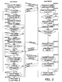
- the controller 100 of the host device 1 first transmits a command for switching an interface voltage (I/F voltage switching command) to the slave device 2 (SH201).
- the controller 200 of the slave device 2 receives the I/F voltage switching command from the host device 1 (SS201), and determines whether the received command is acceptable (SS202), and transmits its response and status to the host device 1.
- the response includes information indicating whether the slave device 2 has correctly accepted the command.
- the status includes information indicating an interface voltage which the slave device 2 can switch to, as well as the current interface voltage of the slave device 2.
- the controller 100 of the host device 1 determines whether the slave device 2 can switch its interface voltage based on the information included in the received response and status signal (SH202). When determining that the switching is impossible, the controller 100 ends the process (SH214). When determining that the switching is possible, the controller 100 instructs the clock control unit 102 to stop outputting clock signals (stops transmission of clock signals from the host device 1 to the slave device 2) and to free the buses 31 and 32 (SH203).
- the controller 100 of the host device 1 controls the clock output terminal unit 110 to output a low-level signal to the bus 30 (SH204).
- the "low level” herein refers to the signal level indicating 0, among the two levels of digital signals: 1 and 0.
- letter L indicates a low-level signal.
- the "high level” refers to the signal level indicating 1, among the two digital signal levels: 1 and 0.
- letter H indicates a high-level signal. The same applies to the description given hereafter.
- the controller 100 of the host device 1 operates to switch the output voltage of the regulator 12 (SH205), and waits until switching of the output voltage is completed while monitoring the voltages of the detection unit (detection circuit) 103 and the stabilization waiting unit (stabilization waiting circuit) 104 (SH206). When determining that the switching has been completed, the host device 1 further waits until a predetermined waiting time elapses (SH207).
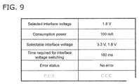
- the predetermined waiting time may be a fixed period of time that is set in advance, a period of time required for switching included in the status information shown in Fig. 9 , or the longer of the two periods.
- the controller 200 of the slave device 2 determines whether it is possible to switch the voltage to the interface voltage indicated by the I/F voltage switching command received from the host device 1 (SS203). When determining that the switching is impossible, the controller 200 of the slave device 2 ends the I/F voltage switching process (SS211). When determining that the switching is possible, the controller 200 instructs the input/output terminal control unit 201 to control the input/output terminal units 211 and 212 to output a low-level signal to the buses 31 and 32 (SS204).
- the controller 200 operates to switch the output voltage of the regulator 22 (SS205), and waits until switching of the output voltage is completed while monitoring the outputs from the detection unit (detection circuit) 203 and the stabilization waiting unit (stabilization waiting circuit) 204 (SS206).
- the controller 100 of the host device 1 instructs the clock control unit 102 to stop the output of low-level signals from the clock output terminal 110 (SH208), and then resumes the clock signal output (for example, the output of clock signals with the interface voltage of, for example, 1.8 V, to which the interface voltage switching has been performed) (resumes transmission of clock signals to the slave device 2) (SH209).
- the clock signal output for example, the output of clock signals with the interface voltage of, for example, 1.8 V, to which the interface voltage switching has been performed
- the controller 200 of the slave device 2 determines whether the voltage switching has been completed in the slave device 2.
- the controller 200 instructs the input/output terminal control unit 201 to output high-level signals (for example, high-level signals having the interface voltage of, for example, 1.8 V, to which the interface voltage switching has been performed) from the input/output terminal units 211 and 212 to the buses 31 and 32 (SS207).
- the controller 200 of the slave device 2 frees the buses 31 and 32 to set these buses to an input state (SS208), and transmits a notification that the interface voltage switching has been completed to the host device 1.
- the slave device 2 can recognize that the interface voltage switching has been completed in the host device 1.
- the buses 31 and 32 are connected to the regulator output (interface voltage) via the pull-up resistors R1 and R2. Thus, when the slave device 2 frees the buses 31 and 32 and sets these buses to an input state, the signal level on the buses 31 and 32 will shift from a low level to a high level in the host device 1.
- the controller 100 of the host device 1 monitors whether the signal level on the buses 31 and 32 is still at a low level after the clock signal output is resumed (SH210), and also determines whether the monitoring time exceeds a predetermined timeout period (SH211). When the timeout period elapses and the signal level on the buses 31 and 32 remains at a low level, the host device 1 determines that an error has occurred, and performs an abnormality processing (SH215). When the signal level on the buses 31 and 32 shifts to a high level before the timeout period elapses, the controller 100 determines that the interface voltage switching has been completed in the slave device 2.
- the host device 1 may further transmit a command to determine whether the switching has been completed successfully.
- the controller 100 transmits a command to perform a switching success/failure determination process (SH212).
- the controller 200 of the slave device 2 receives the switching success/failure determination command from the host device 1 (SS209), determines whether the switching operation of the slave device 2 has been completed (SS210), returns its response and status to the host device 1, and then ends the process (SS211).
- the status includes information indicating the selected interface voltage as shown in Fig. 9 . Alternatively, the information may not be included in the status but may be included in the response.
- the controller 100 of the host device 1 determines whether the interface voltage switching has been completed successfully in the slave device 2 based on the information included in the response and the status received from the slave device 2 (SH213). When determining that the interface voltage switching has been completed successfully in the slave device 2, the controller 100 of the host device 1 ends the interface voltage switching process. When failing to determine that the interface voltage switching has been completed successfully and detecting an abnormality or an error, the controller 100 of the host device 1 performs the abnormality processing (SH215). In the abnormality processing, the host device 1 re-starts (or power-cycles) the slave device 2, and communicates with the slave device 2 through the terminal group 11 of the host device 1 and the terminal group 21 of the slave device 2 using the first interface voltage.
- Fig. 3 is a timing chart illustrating the waveforms of signals on the buses 30, 31, and 32 when the interface voltage of the host device 1 and the slave device 2 is switched with the procedure described based on the flowchart of Fig. 2 in the communication system according to the first embodiment of the present invention.
- the communication system of the present embodiment switches the interface voltage while enabling the host device 1 and the slave device 2 to maintain the electric potentials of the buses in a stable manner.
- the interface voltage is switched from a first interface voltage V1 (for example, 3.3 V) to a second interface voltage V2 ( ⁇ V1) (for example, 1.8 V).
- V1 for example, 3.3 V
- V2 for example, 1.8 V
- the host device 1 issues a command CMD to start a voltage switch sequence (voltage switching process).
- the slave device 2 returns a response to the host device 1.
- the slave device 2 drives the signal level on the bus 31 (bus for transmitting a command CMD in Fig. 3A ) and the bus 32 (bus for transmitting data DAT in Fig. 3A ) to a low level immediately after transmitting the response to the host device 1.
- the host device stops supplying clocks (clocks transmitted on the bus 30) (to the slave device 2). After the host device 1 stops clocks, the slave device 2 starts switching voltage. The time to stop the clocks is not specified.
- the host device 1 can detect whether the interface voltage switching sequence (process) starts by checking the signal level of either the bus 31 (bus for transmitting and receiving a command CMD in Fig. 3A ) or the bus 32 (bus for transmitting and receiving data DAT in Fig. 3A ).
- the host device 1 If low level is not detected, the host device 1 aborts the interface voltage switching sequence, and executes power cycle.
- the voltage to which the switching has been performed which is output from the regulator 22 of the slave device 2 (the second interface voltage V2 of, for example, 1.8 V), shall be stable within a predetermined period T1 (for example 5 ms) (period between t2 and t3 in Fig. 3A ).
- the host device 1 keeps the clocks low at least the predetermined period T1 (for example, 5 ms). This means that the predetermined period T1 (for example, 5 ms) is the maximum value for the slave device 2 and the minimum value for the host device 1.
- the host device 1 starts (resumes) providing clocks at the second interface voltage V2 (for example, 1.8 V).
- the slave device 2 can check whether the voltage of the clocks is the second interface voltage V2 (for example, 1.8 V).
- the slave device 2 drives the signal level on the bus 31 (bus for transmitting and receiving a command CMD in Fig. 3A ) to high at the second interface voltage V2 (for example, 1.8 V) at least one clock and then frees the bus (stops driving the bus) (sets the bus to a high impedance state (tri-state)). For example, outputting a high-level signal and freeing the bus are performed in synchronization with clocks transmitted on the bus 30.
- V2 for example, 1.8 V
- the slave device 2 can check whether the host device 1 drives the voltage on the bus 31 (bus for transmitting and receiving a command CMD in Fig. 3A ) to the second interface voltage V2 (for example, 1.8 V) through the pull-up resistor R1 of the host device 1.
- the buses 31 and 32 are connected to the regulator output (interface voltage) via the pull-up resistors R1 and R2. Thus, when the slave device 2 frees the buses 31 and 32 and sets these buses to an input state, the signal level on the buses 31 and 32 will shift from a low level to a high level in the host device 1.
- the slave device drives the signal level on the bus 32 (bus for transmitting and receiving data DAT in Fig. 3A ) to a high level (stops driving the bus) (sets the bus to a high impedance state) at least a period of one clock cycle and then stop driving (tri-state). For example, outputting a high-level signal and freeing the bus are performed in synchronization with clocks transmitted on the bus 30.
- the signal level on the bus 32 (bus for transmitting and receiving data DAT in Fig. 3A ) is set to a high level within a predetermined period T2 (for example, 1 ms at maximum) (period between t3 and t5 in Fig. 3A ) from the start (resumption) of providing the clocks.
- T2 for example, 1 ms at maximum
- the host device 1 checks whether the signal level on the bus 32 (bus for transmitting and receiving data DAT in Fig. 3A ) is a high level after the predetermined period T2 (for example, after 1 ms) elapses from the start timing at which clocks are provided (timing t3 in Fig. 3 ). This means that the predetermined period T2 (for example, 1 ms at maximum) is a maximum value for the slave device 2, and is a minimum value for the host device 1.
- the host device 1 and the slave device 2 start communicating with each other using the interface voltage to which the switching has been performed.
- the period between t4 and t5 may for example correspond to 1 ms at maximum.
- the communication system of the present embodiment switches the interface voltage while enabling the host device 1 and the slave device 2 to maintain the potentials of the buses in a stable manner.
- Example 1 is a mere example, and the present invention should not be limited to such an example.
- an input/output terminal 112 of the host device 1 and an input/output terminal 212 of the slave device 2 can output a signal as an open drain output.
- the other components are the same as the corresponding components shown in Fig. 1 .
- the slave device 2 operates in accordance with a command transmitted from the host device 1.
- the controller 100 of the host device 1 first transmits a command for switching an interface voltage (I/F voltage switching command) to the slave device 2 (SH401).
- the controller 200 of the slave device 2 receives the I/F voltage switching command from the host device 1 (SS401), determines whether the received command is acceptable (SS402), and transmits its response and status to the host device 1.
- the response and the status include the same information as the information included in the response and the status transmitted from the slave device 2 described in the first embodiment.
- the controller 100 of the host device 1 determines whether the slave device 2 can switch its interface voltage based on the information included in the received response and status signal (SH402). When determining that the switching is impossible, the controller 100 ends the process (SH415). When determining that the switching is possible, the controller 100 instructs the clock control unit 102 to stop outputting clocks (stops transmission of clock signals from the host device 1 to the slave device 2) and to free the buses 31 and 32 (SH403).
- the controller 100 of the host device 1 controls the clock output terminal unit 110 to output a low-level signal to the bus 30, and the input/output terminal unit 112 to output a low-level signal to the bus 32 (SH404).
- the controller 100 of the host device 1 operates to switch the output voltage of the regulator 12 (SH405), and waits until switching of the output voltage is completed while monitoring the outputs from the detection unit (detection circuit) 103 and the stabilization waiting unit (stabilization waiting circuit) 104 (SH406).
- the controller 100 of the host device 1 frees the bus 32 and sets the bus to an input state (SH407).
- the controller 200 of the slave device 2 determines whether it is possible to switch the voltage to the interface voltage indicated by the I/F voltage switching command received from the host device 1 (SS403). When determining that the switching is impossible, the controller 200 of the slave device 2 ends the I/F voltage switching process (SH410). When determining that the switching is possible, the controller 200 instructs the input/output terminal control unit 201 to control the input/output terminal units 211 and 212 to output a low-level signal to the buses 31 and 32 (SS404).
- the controller 200 of the slave device 2 operates to switch the output voltage of the regulator 22 (SS405), and waits until switching of the output voltage is completed while monitoring the outputs from the detection unit (detection circuit) 203 and the stabilization waiting unit (stabilization waiting circuit) 204 (SS406).
- the controller 200 instructs the input/output terminal control unit 201 to free the bus 32 and set the bus to an input state (SS407).
- the signal level on the bus 32 will be at a low level.
- the signal level on the bus 32 will be at a high level, which is determined by the output voltage of the regulator 12 that is connected to the bus 32 via the pull-up resistor R2.
- the input/output terminals 112 and 212 can output a signal as an open drain output, with which both the host device 1 and the slave device 2 can drive the bus to a low level.
- the controller 100 of the host device 1 monitors whether the signal level on the bus 32 is still at a low level (SH408), and also determines whether the monitoring time exceeds a predetermined timeout period (SH409). When the timeout period elapses with the signal level on the bus 32 being maintained at a low level, the host device 1 determines that an error has occurred, and performs abnormality processing (SH415). When the signal level on the bus 32 shifts to a high level before the timeout period elapses, the controller 100 determines that the interface voltage switching has been completed in the slave device 2. In this case, the controller 100 instructs the clock control unit 102 to stop outputting low-level signals from the clock output terminal 110 (SH410), and then resumes the clock signal output (resumes transmission of clock signals to the slave device 2) (SH411).
- the controller 200 of the slave device 2 instructs the input/output terminal control unit 201 to control the input/output terminal unit 211 to output a high-level signal to the bus 31 in synchronization with the clock signals (SS408).
- the controller 200 then frees the bus 31 and sets the bus to an input state (SS409), and transmits a notification that the interface voltage switching has been completed to the host device 1 and ends the process (SS410).
- the slave device 2 When freeing the bus 31, The slave device 2 recognizes that the interface voltage switching has been completed in the host device 1.
- the bus 31 is connected to the regulator output (interface voltage) via the pull-up resistor R1.
- the signal level on the bus 31 will shift from a low level to a high level in the host device 1.
- the controller 100 of the host device 1 monitors whether the signal level on the bus 31 is still at a low level (SH412), and also determines whether the monitoring time exceeds the predetermined timeout period (SH413). This process is performed to detect an abnormality that would prevent the slave device 2 from freeing the bus 31 and setting the bus to an input state.
- the timeout period elapses with the signal level on the bus 31 being maintained at a low level, the host device 1 determines that an error has occurred and performs the abnormality processing (SH415).
- the controller 100 of the host device 1 determines that the interface voltage switching has been completed in the slave device 2, and ends the process (SH414). In the abnormality processing, the host device 1 re-starts (power-cycles) the slave device 2, and communicates with the slave device 2 by operating the terminal group 11 of the host device 1 and the terminal group 21 of the slave device 2 using the first interface voltage.
- the host device 1 may transmit a command to determine whether the switching has been completed successfully to the slave device 2 as described previously with reference to Fig. 2 so as to determine whether the interface voltage switching has been completed successfully in the slave device 2.
- Fig. 5 is a timing chart illustrating the waveforms of signals on the buses 30, 31, and 32 when the interface voltage of the host device 1 and the slave device 2 is switched with the procedure described based on the flowchart of Fig. 4 in the communication system according to the present embodiment.
- symbols "CMD”, “RES”, “Status”, “H”, “L”, and “Z” have the same meanings as those used in Fig. 3 .
- Fig. 5 shows the case in which the interface voltage switching is completed earlier in the host device 1 than in the slave device 2.
- the signal level on the bus 32 is still at a low level after the interface voltage switching is completed in the host device 1 (SH407).
- SH407 the interface voltage switching is completed in the host device 1
- the signal level on the bus 32 will change in the same manner as shown in Fig. 5 .
- the signal level on the bus 32 shifts from L to Z when the interface voltage switching is completed in both the host device 1 and the slave device 2.
- the communication system of the present embodiment switches the interface voltage while enabling the host device 1 and the slave device 2 to maintain the electric potentials of the buses in a stable manner, and also enables the host device 1 and the slave device 2 to determine the completion of each other's voltage switching with a simple method. Also, the communication system of the present embodiment enables the host device 1 and the slave device to immediately determine the completion of each other's processing by monitoring the signal level on the bus 32, and shortens the time required for the voltage switching.
- the components of the host device 1 and the slave device 2 included in the communication system of the present embodiment are the same as the components described with reference to Fig. 1 .
- the slave device 2 operates in accordance with a command transmitted from the host device 1.
- the controller 100 of the host device 1 first transmits a command for switching an interface voltage (I/F voltage switching command) to the slave device 2 (SH601).
- the controller 200 of the slave device 2 receives the I/F voltage switching command from the host device 1 (SS601), and determines whether the received command is acceptable (SS602), and transmits its response and status to the host device 1.
- the response and the status include the same information as the information included in the response and the status described in the first embodiment.
- the controller 100 of the host device 1 determines whether the slave device 2 can switch its interface voltage based on the information included in the received response and status signal (SH602). When determining that the switching is impossible, the controller 100 ends the process (SH614).
- the controller 100 of the host device 1 instructs the clock control unit 102 to stop outputting clocks (stops transmission of clock signals from the host device 1 to the slave device 2) to free the bus 32 (SH603).
- the controller 100 of the host device 1 controls the clock output terminal unit 110 and the input/output terminal unit 111 to output a low-level signal to the buses 30 and 31 (SH604).
- the controller 100 of the host device 1 operates to switch the output voltage of the regulator 12 (SH605), and waits until switching of the output voltage is completed while monitoring the outputs from the detection unit (detection circuit) 103 and the stabilization waiting unit (stabilization waiting circuit) 104 (SH606).
- the host device 1 waits until a predetermined waiting time elapses (SH607).
- the predetermined waiting time may be a fixed period of time that is set in advance, a period of time required for switching included in the status information shown in Fig. 9 , or the longer of the two.
- the controller 200 of the slave device 2 determines whether it is possible to switch the voltage to the interface voltage indicated by the I/F voltage switching command received from the host device 1 (SS603). When determining that the switching is impossible, the controller 200 of the slave device 2 ends the I/F voltage switching process (SS610). When determining that the switching is possible, the controller 200 instructs the input/output terminal control unit 201 to free the bus 31 and set the bus to an input state, and also to output a low-level signal to the bus 32 (SS604).
- the controller 200 of the slave device 2 operates to switch the output voltage of the regulator 22 (SS605), and waits until switching of the output voltage is completed while monitoring the outputs from the detection unit (detection circuit) 203 and the stabilization waiting unit (stabilization waiting circuit) 204 (SS606).
- the controller 100 of the host device 1 instructs the clock control unit 102 to stop the output of low-level signals from the clock output terminal unit 110 (S608), and then resumes the clock signal output (SH609).
- the controller 200 of the slave device 2 instructs the input/output terminal control unit 201 to output a high-level signal from the input/output terminal unit 212 to the bus 32 (SS607) when determining that the voltage switching has been completed.
- the controller 200 then frees the bus 32 and sets the bus to an input state (SS608), and transmits a notification that the interface voltage switching has been completed to the host device 1.
- the bus 32 is connected to the regulator output (interface voltage) via the pull-up resistor 2.
- the signal level on the bus 32 will shift from a low level to a high level in the host device 1.
- the controller 100 of the host device 1 monitors whether the signal level on the bus 32 is still at a low level (SH610), and also determines whether the monitoring time exceeds the predetermined timeout period (SH611). When the timeout period elapses with the signal level on the bus 32 being maintained at a low level, the host device 1 determines that an error has occurred, and performs abnormality processing (SH615).
- the controller 100 of the host device 1 determines that the interface voltage switching has been completed in the slave device 2, and instructs the input/output terminal control unit 101 to output a high-level signal to the bus 31 (SH612) and frees the bus 31 (SH613).
- the slave device 2 determines that the signal level on the bus 31 has shifted to a high level (SS609), and determines that the interface voltage switching has been completed in the host device 1.
- the interface voltage switching is complete both in the host device 1 and the slave device 2.
- the host device 1 may transmit a command to determine whether the switching has been completed successfully.
- the operation of the host device 1 and the slave device 2 in this case is the same as the corresponding operation in the first embodiment described with reference to Fig. 2 .
- Fig. 7 is a timing chart illustrating the waveforms of signals on the buses 30, 31, and 32 when the interface voltage of the host device 1 and the slave device 2 is switched with the procedure described based on the flowchart of Fig. 6 in the communication system according to the present embodiment.
- symbols "CMD”, “RES”, “Status”, “H”, “L”, and “Z” have the same meanings as those used in Fig. 3 .
- the communication system of the present embodiment switches the interface voltage while enabling the host device 1 and the slave device 2 to maintain the electric potentials of the buses in a stable manner, and also enables the host device 1 and the slave device 2 to determine the completion of each other's voltage switching with a simple method.
- Fig. 8 is a flowchart showing the process performed by the slave device 2 for notifying the host device 1 of such an error as well as the process performed by the host device 1 when such an error has occurred in the slave device 2.
- Fig. 8 only shows the steps different from the steps shown in the flowchart of Fig. 2 , and steps that are not shown in Fig. 8 are the same as the corresponding steps shown in Fig. 2 .
- the controller 200 of the slave device 2 determines whether an error has occurred during the interface voltage switching process (SS801). When detecting no error, the controller 200 continues the switching process (SS206). When detecting an error, the controller 200 instructs the input/output terminal control unit 201 to stop outputting a low-level signal to the bus 31 to free the bus 31 (SS802), and ends the process (SS211).
- the host device 1 waits for a voltage switching completion notification from the slave device 2 while monitoring the state of the buses 31 and 32 (SH210).
- SH210 state of the buses 31 and 32
- the host device 1 determines that an error has occurred, and performs abnormality processing (SH215).
- the slave device 2 can notify the host device 1 of an error with a simple method (process) in the communication system.
- the host device 1 then performs the abnormality processing to enable the communication system to recover.
- the regulator 12 of the host device 1 outputs the first interface voltage or the second interface voltage based on the supply voltage from the voltage source 13 in the above embodiments, the present invention should not be limited to this structure.
- the regulator 12 may select an output voltage from a plurality of voltages supplied from a plurality of voltage sources or from a plurality of generated voltages.
- the regulator 22 of the slave device 2 outputs the first interface voltage or the second interface voltage based on the supply voltage from the voltage source 13, the present invention should not be limited to this structure.
- the regulator 22 may select an output voltage from a plurality of voltages supplied from a plurality of voltage sources or from a plurality of generated voltages.
- the host device 1 includes a processing unit for determining the range of interface voltages with which the slave device 2 can operate and a processing unit for instructing the voltage to be used when transmitting an interface voltage switching command from the host device 1 to the slave device 2.
- the bus arrangement of the host device 1 and the slave device 2 should not be limited to the arrangement shown in the block diagram of Fig. 1 .
- the system does not need the clock signals (the bus 30, the input/output terminal units 110 and 111, and the clock control unit 102).
- the bus 31 is used to transmit and receive commands
- the bus 32 is used to transmit and receive data including the status data in the above embodiments
- the present invention should not be limited to this structure.
- the buses may be selected freely for each purpose.
- the number of data buses included in the communication system should not be limited to two.
- the communication system may include, for example, four or eight buses for transmitting and receiving data.
- the slave device 2 may not necessarily return a response and a status when receiving a command transmitted from the host device 1. Instead, the slave device 2 may only transmit a response containing necessary information, or it may not transmit a response.
- the slave device 2 including the interface circuit (interface device) of the present invention may be a removable device, such as a memory card or an input/output card, or may be an LSI device in which a controller LSI, memory, and other functional blocks are enclosed in a single package, which is soldered onto a substrate.
- the host device 1 and the slave device 2 may not necessarily be included in different devices (for example, the host device 1 included in a personal computer and the slave device 2 included in an SD card).
- both the host device 1 and the slave device 2 may be included in a single device (for example, both the host device 1 and the slave device 2 included in a single personal computer or in a single mobile telephone).
- Each block of the communication system, the host device, and the slave device described in the above embodiments may be formed using a single chip with a semiconductor device, such as LSI (large-scale integration), or some or all of the blocks of the communication system, the host device, and the slave device may be formed using a single chip.
- LSI large-scale integration
- an LSI has been described, depending on differences in the degree of integration, it may be also referred to as an IC, system LSI, super LSI, or ultra LSI.
- the circuit integration technology employed should not be limited to LSI, but the circuit integration may be achieved using a dedicated circuit or a general-purpose processor.
- FPGA field programmable gate array
- reconfigurable processor which is an LSI circuit in which internal circuit cells are reconfigurable or more specifically the internal circuit cells can be reconnected or reset, may be used.
- circuit integration technology that can replace LSI emerges as an advancement of the semiconductor technology or as a derivative of the semiconductor technology, the technology may be used to integrate the functional blocks. Biotechnology is potentially applicable.
- the processes described in the above embodiments may be realized using either hardware or software, or may be realized using both software and hardware.
- the communication system, the host device, and the slave device of the above embodiments are implemented by hardware, the communication system, the host device, and the slave device require timing adjustment for each of their processes. For ease of explanation, timing adjustment associated with various signals required in an actual hardware design is not described in detail in the above embodiments.
- the present invention may also be expressed as follows.
- An interface circuit that is used in a host device connected to a slave device to transmit and receive data and/or a command to and from the slave device, the interface circuit comprising:
- the interface circuit according to one of appendixes 1 and 2, wherein the interface voltage switching unit determines that the switching has been completed when the level of the input signal into the input/output terminals becomes a high level.
- An interface circuit that is used in a host device connected to a slave device to transmit and receive data and/or a command to and from the slave device, the interface circuit comprising:
- the interface circuit according to one of appendixes 4 to 6, wherein the interface voltage switching unit determines that the switching has been completed when the level of the input signal into the input/output terminals becomes a high level.
- An interface circuit that is used in a slave device connected to a host device to transmit and receive data and/or a command to and from the host device, the interface circuit comprising:
- the interface circuit according to appendix 8 wherein the input/output terminal control unit controls all the input/output terminals to be in the low level output status.
- the interface circuit according to appendix 8 wherein the interface voltage switching unit determines that the interface voltage switching has been completed in the host device when switching the input/output terminals from the low level output status to the input status in synchronization with the clock input.
- the interface circuit according to appendix 8 wherein the interface voltage switching unit determines that the interface voltage switching has been completed in the host device when a signal indicating completion of the switching is input into the input/output terminals after switching the input/output terminals from the low level output status to the input status in synchronization with the clock input.
- the interface circuit according to appendix 8 wherein the interface voltage switching unit switches the input/output terminals from the low level output status to the input status in synchronization with the clock input when the interface voltage switching has been completed in the slave device.
- the interface circuit according to appendix 8 wherein the interface voltage switching unit switches at least one of the input/output terminals that are in the low level output status to the input status when the interface voltage switching has been completed, and switches the remaining input/output terminals that are in the low level output status to the input status in synchronization with the clock input from the host device.
- the interface circuit according to appendix 8 wherein the input/output terminal control unit outputs a signal from the input/output terminals as an open drain output.
- the interface circuit according to appendix 8 wherein when the interface voltage switching is terminated incompletely due to an abnormality, the interface voltage switching unit switches a command transmission/reception terminal from the low level output status to the input status after a predetermined period elapses.
- the interface circuit according to one of appendixes 8 to 15, wherein the interface voltage switching unit determines that the switching has been completed when the level of the input signal into the input/output terminals becomes a high level.
- a host device comprising:
- the host device according to appendix 17, wherein the host device transmits a command to obtain a time required for the interface voltage switching by the slave device before the interface voltage switching is started.
- the host device according to appendix 17, wherein the host device transmits a command to determine whether the interface voltage switching has been completed successfully after the interface voltage switching is completed.
- a host device comprising:
- the host device according to appendix 20, wherein the host device transmits a command to obtain a time required for the interface voltage switching by the slave device before the interface voltage switching is started.
- the host device according to appendix 20, wherein the host device transmits a command to determine whether the interface voltage switching has been completed successfully after the interface voltage switching is completed.
- a slave device comprising:
- a response to a command transmitted from the host device includes a maximum value of a time required for the interface voltage switching.
- a response to a command transmitted from the host device includes status information indicating that the interface voltage switching has been completed successfully.
- a communication system comprising:
- a communication system comprising:
- the interface circuit (device) of the present invention enable an interface voltage to be switched while enabling the host device and the slave device to maintain the signal level of buses in a stable manner.
- the present invention is therefore applicable to a communication system in which an interface voltage can be switched using a small number of signal lines.
Landscapes
- Engineering & Computer Science (AREA)
- Theoretical Computer Science (AREA)
- Physics & Mathematics (AREA)
- General Engineering & Computer Science (AREA)
- General Physics & Mathematics (AREA)
- Power Sources (AREA)
Claims (12)
- Dispositif d'interface qui est utilisé dans un dispositif hôte relié à un dispositif esclave pour transmettre et recevoir des données et/ou une commande audit et en provenance dudit dispositif esclave, et qui commute une tension d'interface utilisée pour la communication entre le dispositif esclave et le dispositif hôte, le dispositif d'interface comprenant;
une unité de sortie d'horloge qui délivre un signal d'horloge pour transmettre et recevoir les données et/ou la commande,
un groupe de terminaux comprenant une ou plusieurs unités de terminal d'entrée/de sortie, qui transmet et reçoit les données et/ou la commande en utilisant une parmi une première tension d'interface et une deuxième tension d'interface; et
une unité de commutation de tension d'interface qui choisit l'une parmi la première tension d'interface et la deuxième tension d'interface et commute, à celle choisie parmi les première et deuxième tensions d'interface, la tension d'interface utilisée pour la communication entre le dispositif hôte et le dispositif esclave,
dans lequel ladite unité de commutation de tension d'interface comprend
une unité de commande,
une unité de commande d'horloge qui est commandée par ladite unité de commande et fixe un niveau d'une sortie de signal en provenance de ladite unité de sortie d'horloge à un premier niveau de signal lorsque la tension d'interface utilisée pour la communication entre le dispositif hôte et le dispositif esclave est à commuter; et qui, lorsqu'une tension d'interface dans le dispositif hôte a été commutée à la tension d'interface choisie, commande ladite unité de sortie d'horloge pour délivrer un signal d'horloge en utilisant la tension d'interface choisie, et
une unité de commande de terminal d'entrée/de sortie, commandée par l'unité de commande, ladite unité de commande de terminal d'entrée/de sortie mettant ladite une ou lesdites plusieurs unités de terminal d'entrée/de sortie dans un état d'entrée, surveillant un niveau d'un signal d'entrée dans ladite une ou lesdites plusieurs unités de terminal d'entrée/de sortie lorsque la tension d'interface utilisée pour la communication entre le dispositif hôte et le dispositif esclave est à commuter, et transmettant - lorsque t'unité de commande de terminal d'entrée/de sortie détecte que le niveau du signal d'entrée dans ladite une ou lesdites plusieurs unités de terminal d'entrée/de sortie devient un niveau de signal indiquant qu'une tension d'interface dans le dispositif esclave a été commutée à la tension d'interface choisie - à ladite unité de commande une notification indiquant le résultat de détection,
et ladite unité de commande détermine que la tension d'interface dans le dispositif esclave a été commutée, lorsque la notification est reçue qui indique que la commutation de la tension d'interface a été achevée dans le dispositif esclave et qui a été transmise depuis l'unité de commande de terminal d'entrée/de sortie après que l'unité de commande d'horloge à été mise dans un état où le signal d'horloge est délivré en utilisant la tension d'interface choisie. - Dispositif d'interface selon la revendication 1, dans lequel le premier niveau de signal est un faible niveau.
- Dispositif d'interface selon l'une quelconque des revendications 1 et 2, dans lequel ladite unité de commande met l'ensemble des unités de terminal d'entrée/de sortie dans un état d'entrée, lorsque la tension d'interface utilisée pour la communication entre le dispositif hôte et le dispositif esclave est à commuter.
- Dispositif d'interface selon l'une quelconque des revendications 1 à 3, dans lequel ladite unité de commande détermine que la tension d'interface dans le dispositif hôte et la tension d'interface dans le dispositif esclave ont été commutées, lorsque le niveau du signal d'entrée dans les unités de terminal d'entrée/de sortie devient un haut niveau sur la tension d'interface choisie.
- Dispositif d'interface qui est utilisé dans un dispositif esclave relié à un dispositif hôte pour transmettre et recevoir des données et/ou une commande audit et en provenance dudit dispositif hôte, et qui commute une tension d'interface utilisée pour la communication entre le dispositif esclave et le dispositif hôte, le dispositif d'interface comprenant:une unité d'entrée d'horloge qui reçoit une entrée d'un signal d'horloge pour transmettre et recevoir les données et/ou la commande;un groupe de terminaux comprenant une ou plusieurs unités de terminal d'entrée/de sortie, qui transmet et reçoit les données et/ou la commande en utilisant une parmi une première tension d'interface et une deuxième tension d'interface; etune unité de commutation de tension d'interface qui choisit l'une parmi la première tension d'interface et la deuxième tension d'interface et commute, à celle choisie parmi les première et deuxième tensions d'interface, la tension d'interface utilisée pour la communication entre le dispositif hôte et le dispositif esclave,dans lequel ladite unité de commutation de tension d'interface comprendune unité de commande,et une unité de commande de terminal d'entrée/de sortie, commandée par l'unité de commande, ladite unité de commande de terminal d'entrée/de sortie mettant ladite une ou lesdites plusieurs unités de terminal d'entrée/de sortie dans un état de sortie à un premier niveau de signal lorsque la tension d'interface utilisée pour la communication entre le dispositif hôte et le dispositif esclave est à commuter, et commutant, lorsqu'une tension d'interface dans le dispositif esclave a été commutée à la tension d'interface choisie, ladite une ou lesdites plusieurs unités de terminal d'entrée/de sortie de l'état de sortie au premier niveau de signal à un état d'entrée.
- Dispositif d'interface selon la revendication 5, dans lequel ladite unité de commande de terminal d'entrée/de sortie met l'ensemble des unités de terminal d'entrée/de sortie dans l'état de sortie au premier niveau de signal, lorsque la tension d'interface utilisée pour la communication entre le dispositif hôte et le dispositif esclave est à commuter.
- Dispositif d'interface selon l'une quelconque des revendications 5 et 6, dans lequel ladite unité de commutation de tension d'interface détermine qu'une tension d'interface dans le dispositif hôte a été commutée à la tension d'interface choisie, en commutant les unités de terminal d'entrée/de sortie de l'état de sortie au premier niveau de signale l'état d'entrée en synchronisation avec le signal d'horloge entré dans ladite unité d'entrée d'horloge.
- Dispositif d'interface selon l'une quelconque des revendications 5 et 6, dans lequel ladite unité de commutation de tension d'interface commute au moins l'une des unités de terminal d'entrée/de sortie qui sont dans l'état de sortie au premier niveau de signal, à l'état d'entrée, lorsque la tension d'interface a été commutée, et commute les unités restantes de terminal d'entrée/de sortie qui sont dans l'état de sortie au premier niveau de signal, à l'état d'entrée en synchronisation avec le signal d'horloge entré dans l'unité d'entrée d'horloge.
- Dispositif hôte comprenant:le dispositif d'interface selon l'une quelconque des revendications 1 à 4, dans lequel le dispositif hôte est relié à un dispositif esclave via le dispositif d'interface afin de transmettre et recevoir des données et/ou une commande audit et en provenance dudit dispositif esclave.
- Dispositif esclave comprenant:le dispositif d'interface selon l'une quelconque des revendications 5 à 8, dans lequel le dispositif esclave est relié à un dispositif hôte via le dispositif d'interface afin de transmettre et recevoir des données et/ou une commande audit et en provenance dudit dispositif hôte.
- Procédé de commutation de tension d'interface destiné à commuter une tension d'interface utilisée pour la communication entre un dispositif hôte et un dispositif esclave, le procédé comprenant:le dispositif hôte fournit une commande donnant l'instruction de commuter une tension d'interface sur le dispositif esclave,le dispositif esclave donne une réponse la commande, qui donne l'instruction de commuter la tension d'interface sur le dispositif hôte,le dispositif hôte arrête de fournir un signal d'horloge, en fixant, à un premier niveau de signal, un niveau d'une sortie de signal d'horloge à destination du dispositif esclave;le dispositif hôte met une ou plusieurs unités de terminal d'entrée/de sortie se trouvant dans le dispositif hôte, dans un état d'entrée:le dispositif esclave met un ou plusieurs terminaux d'entrée/de sortie se trouvant dans le dispositif esclave, dans un état de sortie au premier niveau de signal;le dispositif esclave fait passer lesdits terminaux d'entrée/de sortie du dispositif esclave de l'état de sortie au premier niveau de signal à l'état d'entrée, lorsqu'une tension d'interface a été commutée dans le dispositif esclave;le dispositif hôte recommence à fournir le signal d'horloge lorsque la tension d'interface a été commutée dans le dispositif hôte; etle dispositif hôte détecte qu'un signal indiquant l'achèvement de la commutation de tension d'interface dans le dispositif esclave a été entré dans les terminaux d'entrée/de sortie du dispositif hôte, après avoir recommencé la sortie d'horloge, et détermine que la tension d'interface a été commutée dans le dispositif esclave.
- Procédé de commutation de tension d'interface destiné à commuter une tension d'interface utilisée pour la communication entre un dispositif hôte et un dispositif esclave qui communiquent entre eux d'une première tension d'interface V1 à une deuxième tension d'interface V2 via un premier bus pour transmettre un signal d'horloge, un deuxième bus pour transmettre une commande et via un troisième bus pour transmettre des données, le procédé comprenant:(1) le dispositif hôte fournit une commande CMD au dispositif esclave pour démarrer une séquence de commutation de tension d'interface;(2) le dispositif esclave donne, au dispositif hôte, une réponse à la commande CMD;(3) le dispositif esclave met un niveau de signal du deuxième bus et du troisième bus, immédiatement après la transmission de la réponse au dispositif hôte, à un faible niveau;(4) le dispositif hôte arrête de fournir le signal d'horloge au dispositif esclave, le dispositif esclave démarre un processus pour commuter la tension d'interface, après que le dispositif hôte a arrêté de fournir le signal d'horloge, le dispositif hôte détecte si la séquence de commutation de tension d'interface commence, en surveillant un niveau de signal de l'un parmi le deuxième bus et le troisième bus, et le dispositif hôte interrompt la séquence de commutation de tension d'interface et met en oeuvre un cycle de puissance (power cycle) lorsqu'il ne parvient pas à détecter un faible niveau en tant que niveau de signal de l'un des deuxième et troisième bus;(5) le dispositif esclave stabilise une tension d'interface pour laquelle le processus de commutation de la tension d'interface a été mis en oeuvre, laquelle a été sortie par un régulateur se trouvant dans le dispositif esclave, dans une période T1 prédéterminée, et le dispositif hôte fixe, à un faible niveau, un niveau du signal d'horloge pour au moins la période T1 prédéterminée;(6) le dispositif hôte recommence à fournir un signal d'horloge à la deuxième tension d'interface V2 lorsqu'une sortie de tension d'un régulateur se trouvant dans le dispositif hôte s'est stabilisée après que la période T1 prédéterminée s'est écoulée à partir de la fin de l'étape (4), et le dispositif esclave vérifie si le niveau du signal d'horloge est un niveau de signal qui est basé sur la deuxième tension d'interface V2;(7) le dispositif esclave détecte le signal d'horloge et met un niveau de signal du deuxième bus à un haut niveau pour au moins une période d'un cycle d'horloge du signal d'horloge, en utilisant la deuxième tension d'interface V2, et libère ensuite le deuxième bus;(8) le dispositif esclave vérifie si le dispositif hôte met le niveau de signal du deuxième bus à ladite deuxième tension d'interface V2 par une résistance de pull-up R1 reliée au deuxième bus du dispositif hôte; et(9) le dispositif esclave met le niveau de signal du troisième bus à un haut niveau pour au moins une période d'un cycle d'horloge et libère ensuite le troisième bus lorsque le processus de commutation de la tension d'interface a été achevé avec succès, le niveau de signal du troisième bus étant mis à un haut niveau dans une période T2 prédéterminée à partir du recommencement de la fourniture du signal d'horloge, et le dispositif hôte vérifie si le niveau de signal du troisième bus est un haut niveau après que la période T2 prédéterminée s'est écoulée à partir d'un moment t3 où la fourniture de l'horloge a commencé.
Applications Claiming Priority (2)
| Application Number | Priority Date | Filing Date | Title |
|---|---|---|---|
| JP2008049360 | 2008-02-29 | ||
| PCT/JP2009/000908 WO2009107400A1 (fr) | 2008-02-29 | 2009-02-27 | Dispositif d'interface pour dispositif hôte, dispositif d'interface pour dispositif esclave, dispositif hôte, dispositif esclave, système de communication et procédé de commutation de tension d'interface |
Publications (3)
| Publication Number | Publication Date |
|---|---|
| EP2249227A1 EP2249227A1 (fr) | 2010-11-10 |
| EP2249227A4 EP2249227A4 (fr) | 2014-06-25 |
| EP2249227B1 true EP2249227B1 (fr) | 2015-05-27 |
Family
ID=41015807
Family Applications (1)
| Application Number | Title | Priority Date | Filing Date |
|---|---|---|---|
| EP09713710.3A Active EP2249227B1 (fr) | 2008-02-29 | 2009-02-27 | Dispositif d'interface pour dispositif hôte, dispositif d'interface pour dispositif esclave, dispositif hôte, dispositif esclave, système de communication et procédé de commutation de tension d'interface |
Country Status (5)
| Country | Link |
|---|---|
| US (3) | US8067861B2 (fr) |
| EP (1) | EP2249227B1 (fr) |
| JP (2) | JP5186548B2 (fr) |
| CN (1) | CN101910972B (fr) |
| WO (1) | WO2009107400A1 (fr) |
Cited By (1)
| Publication number | Priority date | Publication date | Assignee | Title |
|---|---|---|---|---|
| EP3170059A1 (fr) * | 2014-07-15 | 2017-05-24 | Kabushiki Kaisha Toshiba | Appareil hôte et dispositif d'extension |
Families Citing this family (20)
| Publication number | Priority date | Publication date | Assignee | Title |
|---|---|---|---|---|
| US9798370B2 (en) * | 2009-03-30 | 2017-10-24 | Lenovo (Singapore) Pte. Ltd. | Dynamic memory voltage scaling for power management |
| US8645772B2 (en) * | 2010-08-25 | 2014-02-04 | Itron, Inc. | System and method for managing uncertain events for communication devices |
| US8892922B2 (en) * | 2010-11-30 | 2014-11-18 | Apple Inc. | Voltage detection |
| WO2013059987A1 (fr) * | 2011-10-25 | 2013-05-02 | 深圳市海思半导体有限公司 | Procédé de réduction de consommation dynamique d'énergie et dispositif électronique |
| JP5527830B2 (ja) * | 2012-08-30 | 2014-06-25 | Necインフロンティア株式会社 | 主装置間インターフェース装置、それを含む主装置システム及び主装置間インターフェース方法 |
| WO2015159486A1 (fr) * | 2014-04-17 | 2015-10-22 | パナソニック インテレクチュアル プロパティ コーポレーション オブ アメリカ | Système de réseau monté dans un véhicule, unité de commande électronique de détection d'invalidité, et procédé de détection d'invalidité |
| WO2016132733A1 (fr) * | 2015-02-16 | 2016-08-25 | パナソニックIpマネジメント株式会社 | Dispositif hôte, dispositif esclave, dispositif d'interface à semi-conducteur, et système amovible |
| US10454412B2 (en) * | 2015-07-31 | 2019-10-22 | International Business Machines Corporation | Tunable photonic harvesting for solar energy conversion and dynamic shading tolerance |
| JP2017097825A (ja) * | 2015-11-16 | 2017-06-01 | 株式会社東芝 | ホスト機器および拡張デバイス |
| JP6620313B2 (ja) * | 2016-01-06 | 2019-12-18 | パナソニックIpマネジメント株式会社 | ホスト装置、スレーブ装置及びリムーバブルシステム |
| US10339083B2 (en) | 2016-01-06 | 2019-07-02 | Panasonic Intellectual Property Management Co., Ltd. | Host device, slave device, and removable system |
| JP6214709B2 (ja) | 2016-03-31 | 2017-10-18 | キヤノン株式会社 | アクセサリ装置、撮像装置および通信制御プログラム |
| KR102730323B1 (ko) * | 2016-12-22 | 2024-11-15 | 삼성전자주식회사 | 전자 장치 및 그의 에러 검출 방법 |
| US11157064B2 (en) | 2017-09-28 | 2021-10-26 | Intel Corporation | Techniques to dynamically enable and disable accelerator devices in compute environments |
| KR102728195B1 (ko) | 2018-11-09 | 2024-11-08 | 삼성전자주식회사 | 호스트와 통신을 수행하는 전자 장치 및 그 동작 방법 |
| CN111572596B (zh) * | 2020-06-04 | 2024-08-09 | 哈尔滨铁路减速顶调速研究有限公司 | 一种机车信号主机输出信息在车检测系统 |
| EP4254211A4 (fr) * | 2020-11-24 | 2024-05-01 | Panasonic Intellectual Property Management Co., Ltd. | Dispositif hôte, dispositif esclave et système de transfert de données |
| EP4296863A4 (fr) * | 2021-02-16 | 2024-08-07 | Panasonic Intellectual Property Management Co., Ltd. | Dispositif hôte, dispositif esclave et système de transfert de données |
| TWI789147B (zh) * | 2021-12-07 | 2023-01-01 | 瑞昱半導體股份有限公司 | 讀卡裝置及具有讀卡功能的電子裝置 |
| CN118742873A (zh) | 2022-02-22 | 2024-10-01 | 松下知识产权经营株式会社 | 主机装置、从机装置以及主从系统 |
Family Cites Families (32)
| Publication number | Priority date | Publication date | Assignee | Title |
|---|---|---|---|---|
| US5734585A (en) * | 1994-11-07 | 1998-03-31 | Norand Corporation | Method and apparatus for sequencing power delivery in mixed supply computer systems |
| US6078319A (en) * | 1995-04-17 | 2000-06-20 | Cirrus Logic, Inc. | Programmable core-voltage solution for a video controller |
| US5894238A (en) * | 1997-01-28 | 1999-04-13 | Chien; Pien | Output buffer with static and transient pull-up and pull-down drivers |
| US6515507B1 (en) * | 1999-07-01 | 2003-02-04 | Altera Corporation | Control pin for specifying integrated circuit voltage levels |
| US6512401B2 (en) * | 1999-09-10 | 2003-01-28 | Intel Corporation | Output buffer for high and low voltage bus |
| JP2001093275A (ja) * | 1999-09-20 | 2001-04-06 | Mitsubishi Electric Corp | 半導体集積回路装置 |
| KR20020050270A (ko) | 1999-11-09 | 2002-06-26 | 토토라노 제이. 빈센트 | 환경에 따른 프로세서의 작동 파라미터의 동적 조절방법 |
| JP4649009B2 (ja) * | 2000-03-08 | 2011-03-09 | 株式会社東芝 | カードインタフェースを備えた情報処理装置、同装置に装着可能なカード型電子機器、及び同装置におけ動作モード設定方法 |
| JP3461323B2 (ja) * | 2000-03-28 | 2003-10-27 | シャープ株式会社 | Pcカード |
| US6721892B1 (en) * | 2000-05-09 | 2004-04-13 | Palmone, Inc. | Dynamic performance adjustment of computation means |
| US6664775B1 (en) * | 2000-08-21 | 2003-12-16 | Intel Corporation | Apparatus having adjustable operational modes and method therefore |
| US6952112B2 (en) * | 2000-11-30 | 2005-10-04 | Renesas Technology Corporation | Output buffer circuit with control circuit for modifying supply voltage and transistor size |
| JP2002169631A (ja) | 2000-11-30 | 2002-06-14 | Hitachi Ltd | 情報処理装置およびi/oカード |
| JP3976237B2 (ja) * | 2002-02-13 | 2007-09-12 | シャープ株式会社 | 半導体記憶装置および電子情報機器 |
| US20040128565A1 (en) * | 2002-12-31 | 2004-07-01 | Intel Corporation (A Delaware Corporation) | System for driving clock signal over a bus for a slave device |
| AU2003283550A1 (en) * | 2003-01-13 | 2004-08-10 | Arm Limited | Data processing performance control |
| CN1519679B (zh) * | 2003-01-21 | 2010-04-28 | 英业达股份有限公司 | 调整中央处理器工作频率的装置及其方法 |
| US7290161B2 (en) * | 2003-03-24 | 2007-10-30 | Intel Corporation | Reducing CPU and bus power when running in power-save modes |
| JP4653960B2 (ja) * | 2003-08-07 | 2011-03-16 | ルネサスエレクトロニクス株式会社 | メモリカードおよび不揮発性メモリ混載マイコン |
| KR100560767B1 (ko) * | 2003-09-02 | 2006-03-13 | 삼성전자주식회사 | 탈착 가능한 저장 장치를 포함하는 시스템 및 그것의 제어방법 |
| KR100884235B1 (ko) * | 2003-12-31 | 2009-02-17 | 삼성전자주식회사 | 불휘발성 메모리 카드 |
| US7698575B2 (en) * | 2004-03-30 | 2010-04-13 | Intel Corporation | Managing power consumption by requesting an adjustment to an operating point of a processor |
| US7180813B2 (en) * | 2004-12-15 | 2007-02-20 | Stmicroelectronics, Inc. | Programmable system device having a shared power supply voltage generator for FLASH and PLD modules |
| US7246027B2 (en) * | 2005-03-11 | 2007-07-17 | Sigmatel, Inc. | Power optimization of a mixed-signal system on an integrated circuit |
| JP2006276967A (ja) * | 2005-03-28 | 2006-10-12 | Renesas Technology Corp | 半導体装置 |
| US20090077393A1 (en) | 2005-04-27 | 2009-03-19 | Matsushita Electric Industrial Co., Ltd. | Card-type electronic device and host device |
| US7522941B2 (en) * | 2005-05-23 | 2009-04-21 | Broadcom Corporation | Method and apparatus for reducing standby power consumption of a handheld communication system |
| US7707435B2 (en) * | 2005-06-16 | 2010-04-27 | Broadcom Corporation | Method and system for safe and efficient chip power down drawing minimal current when a device is not enabled |
| US7212463B2 (en) * | 2005-09-23 | 2007-05-01 | Sigma Tel, Inc. | Method and system of operating mode detection |
| US8051231B2 (en) * | 2008-11-06 | 2011-11-01 | International Business Machines Corporation | Data communications among electronic devices within a computer |
| WO2011070747A1 (fr) * | 2009-12-07 | 2011-06-16 | パナソニック株式会社 | Dispositif de stockage non volatil, dispositif hôte, systeme de stockage, procede de communication de donnees et programme |
| JP5789759B2 (ja) * | 2010-03-16 | 2015-10-07 | パナソニックIpマネジメント株式会社 | 情報処理装置、不揮発性記憶装置、情報処理システム及び不揮発性メモリコントローラ |
-
2009
- 2009-02-27 CN CN2009801017789A patent/CN101910972B/zh active Active
- 2009-02-27 EP EP09713710.3A patent/EP2249227B1/fr active Active
- 2009-02-27 US US12/810,521 patent/US8067861B2/en active Active
- 2009-02-27 WO PCT/JP2009/000908 patent/WO2009107400A1/fr not_active Ceased
- 2009-02-27 JP JP2010500579A patent/JP5186548B2/ja active Active
-
2011
- 2011-10-13 US US13/272,563 patent/US8207638B2/en active Active
- 2011-10-13 US US13/272,534 patent/US8212429B2/en active Active
-
2012
- 2012-12-14 JP JP2012273561A patent/JP5395948B2/ja active Active
Cited By (1)
| Publication number | Priority date | Publication date | Assignee | Title |
|---|---|---|---|---|
| EP3170059A1 (fr) * | 2014-07-15 | 2017-05-24 | Kabushiki Kaisha Toshiba | Appareil hôte et dispositif d'extension |
Also Published As
| Publication number | Publication date |
|---|---|
| JP5395948B2 (ja) | 2014-01-22 |
| US8212429B2 (en) | 2012-07-03 |
| WO2009107400A1 (fr) | 2009-09-03 |
| CN101910972B (zh) | 2013-03-20 |
| CN101910972A (zh) | 2010-12-08 |
| JPWO2009107400A1 (ja) | 2011-06-30 |
| US20100264753A1 (en) | 2010-10-21 |
| EP2249227A4 (fr) | 2014-06-25 |
| US20120032528A1 (en) | 2012-02-09 |
| JP2013101636A (ja) | 2013-05-23 |
| US8207638B2 (en) | 2012-06-26 |
| US20120033717A1 (en) | 2012-02-09 |
| EP2249227A1 (fr) | 2010-11-10 |
| US8067861B2 (en) | 2011-11-29 |
| JP5186548B2 (ja) | 2013-04-17 |
Similar Documents
| Publication | Publication Date | Title |
|---|---|---|
| EP2249227B1 (fr) | Dispositif d'interface pour dispositif hôte, dispositif d'interface pour dispositif esclave, dispositif hôte, dispositif esclave, système de communication et procédé de commutation de tension d'interface | |
| KR102035986B1 (ko) | 타이밍 컨트롤러와 상기 타이밍 컨트롤러를 포함하는 디스플레이 시스템 | |
| US9342131B2 (en) | USB hub and control method of USB hub | |
| US8160645B2 (en) | Apparatus and method for supporting SIM card in mobile communication terminal having multiple modems | |
| US10073800B2 (en) | Coupling controller, information processing apparatus and coupling control method | |
| EP4449265B1 (fr) | Changement de configuration d'interface de couche physique d'interface série d'affichage dynamique | |
| CN110444156B (zh) | 显示装置及其驱动器 | |
| JP2009140483A (ja) | メモリカード制御装置およびメモリカード制御方法 | |
| US7818469B2 (en) | USB device and peripheral device changing functional module to activate in accordance with descriptor | |
| WO2008075311A2 (fr) | Génération d'horloge pour accès mémoire sans oscillateur local | |
| US8897705B2 (en) | Data transmitting system and data transmitting method | |
| US20040083400A1 (en) | Clock control circuit, data transfer control device, and electronic equipment | |
| WO2023159415A1 (fr) | Signalisation adaptative à faible puissance pour permettre une récupération d'erreur de signal de liaison sans taux d'horloge de liaison accrus | |
| US12079071B2 (en) | Programmable initial packets rejection in a display system interface | |
| WO2023240532A1 (fr) | Îlot basse puissance destiné à une interface d'affichage | |
| KR102254255B1 (ko) | 싱글 와이어 인터페이스를 포함하는 장치와 이를 포함하는 데이터 처리 시스템 | |
| US20240323992A1 (en) | Runtime adjustment and sequential calibration of display communication interface drive strength to improve wireless network signal quality | |
| US12093116B2 (en) | Programmable hot plug-in controller for a multidrop differential serial bus | |
| US20260079873A1 (en) | Transmission circuit, reception circuit, transmission and reception circuit, and communication device | |
| WO2024124520A1 (fr) | Transmission hsync hybride pour panneaux d'affichage en mode vidéo | |
| US20030009614A1 (en) | Method for selecting an expansion device in a computer unit, a circuit board, and a computer | |
| JP2009199106A (ja) | インターフェース回路、該インターフェース回路を備えた電子機器、通信システム、及び電圧切り替え方法 |
Legal Events
| Date | Code | Title | Description |
|---|---|---|---|
| PUAI | Public reference made under article 153(3) epc to a published international application that has entered the european phase |
Free format text: ORIGINAL CODE: 0009012 |
|
| 17P | Request for examination filed |
Effective date: 20100705 |
|
| AK | Designated contracting states |
Kind code of ref document: A1 Designated state(s): AT BE BG CH CY CZ DE DK EE ES FI FR GB GR HR HU IE IS IT LI LT LU LV MC MK MT NL NO PL PT RO SE SI SK TR |
|
| AX | Request for extension of the european patent |
Extension state: AL BA RS |
|
| DAX | Request for extension of the european patent (deleted) | ||
| A4 | Supplementary search report drawn up and despatched |
Effective date: 20140526 |
|
| RIC1 | Information provided on ipc code assigned before grant |
Ipc: G06F 1/26 20060101AFI20140520BHEP |
|
| GRAP | Despatch of communication of intention to grant a patent |
Free format text: ORIGINAL CODE: EPIDOSNIGR1 |
|
| INTG | Intention to grant announced |
Effective date: 20141210 |
|
| GRAS | Grant fee paid |
Free format text: ORIGINAL CODE: EPIDOSNIGR3 |
|
| GRAA | (expected) grant |
Free format text: ORIGINAL CODE: 0009210 |
|
| AK | Designated contracting states |
Kind code of ref document: B1 Designated state(s): AT BE BG CH CY CZ DE DK EE ES FI FR GB GR HR HU IE IS IT LI LT LU LV MC MK MT NL NO PL PT RO SE SI SK TR |
|
| REG | Reference to a national code |
Ref country code: GB Ref legal event code: FG4D |
|
| REG | Reference to a national code |
Ref country code: CH Ref legal event code: EP |
|
| REG | Reference to a national code |
Ref country code: AT Ref legal event code: REF Ref document number: 729175 Country of ref document: AT Kind code of ref document: T Effective date: 20150615 |
|
| REG | Reference to a national code |
Ref country code: IE Ref legal event code: FG4D |
|
| REG | Reference to a national code |
Ref country code: DE Ref legal event code: R096 Ref document number: 602009031417 Country of ref document: DE |
|
| REG | Reference to a national code |
Ref country code: AT Ref legal event code: MK05 Ref document number: 729175 Country of ref document: AT Kind code of ref document: T Effective date: 20150527 |
|
| REG | Reference to a national code |
Ref country code: LT Ref legal event code: MG4D |
|
| PG25 | Lapsed in a contracting state [announced via postgrant information from national office to epo] |
Ref country code: NO Free format text: LAPSE BECAUSE OF FAILURE TO SUBMIT A TRANSLATION OF THE DESCRIPTION OR TO PAY THE FEE WITHIN THE PRESCRIBED TIME-LIMIT Effective date: 20150827 Ref country code: ES Free format text: LAPSE BECAUSE OF FAILURE TO SUBMIT A TRANSLATION OF THE DESCRIPTION OR TO PAY THE FEE WITHIN THE PRESCRIBED TIME-LIMIT Effective date: 20150527 Ref country code: PT Free format text: LAPSE BECAUSE OF FAILURE TO SUBMIT A TRANSLATION OF THE DESCRIPTION OR TO PAY THE FEE WITHIN THE PRESCRIBED TIME-LIMIT Effective date: 20150928 Ref country code: LT Free format text: LAPSE BECAUSE OF FAILURE TO SUBMIT A TRANSLATION OF THE DESCRIPTION OR TO PAY THE FEE WITHIN THE PRESCRIBED TIME-LIMIT Effective date: 20150527 Ref country code: HR Free format text: LAPSE BECAUSE OF FAILURE TO SUBMIT A TRANSLATION OF THE DESCRIPTION OR TO PAY THE FEE WITHIN THE PRESCRIBED TIME-LIMIT Effective date: 20150527 Ref country code: FI Free format text: LAPSE BECAUSE OF FAILURE TO SUBMIT A TRANSLATION OF THE DESCRIPTION OR TO PAY THE FEE WITHIN THE PRESCRIBED TIME-LIMIT Effective date: 20150527 |
|
| REG | Reference to a national code |
Ref country code: NL Ref legal event code: MP Effective date: 20150527 |
|
| PG25 | Lapsed in a contracting state [announced via postgrant information from national office to epo] |
Ref country code: IS Free format text: LAPSE BECAUSE OF FAILURE TO SUBMIT A TRANSLATION OF THE DESCRIPTION OR TO PAY THE FEE WITHIN THE PRESCRIBED TIME-LIMIT Effective date: 20150927 Ref country code: BG Free format text: LAPSE BECAUSE OF FAILURE TO SUBMIT A TRANSLATION OF THE DESCRIPTION OR TO PAY THE FEE WITHIN THE PRESCRIBED TIME-LIMIT Effective date: 20150827 Ref country code: AT Free format text: LAPSE BECAUSE OF FAILURE TO SUBMIT A TRANSLATION OF THE DESCRIPTION OR TO PAY THE FEE WITHIN THE PRESCRIBED TIME-LIMIT Effective date: 20150527 Ref country code: GR Free format text: LAPSE BECAUSE OF FAILURE TO SUBMIT A TRANSLATION OF THE DESCRIPTION OR TO PAY THE FEE WITHIN THE PRESCRIBED TIME-LIMIT Effective date: 20150828 Ref country code: LV Free format text: LAPSE BECAUSE OF FAILURE TO SUBMIT A TRANSLATION OF THE DESCRIPTION OR TO PAY THE FEE WITHIN THE PRESCRIBED TIME-LIMIT Effective date: 20150527 |
|
| PG25 | Lapsed in a contracting state [announced via postgrant information from national office to epo] |
Ref country code: EE Free format text: LAPSE BECAUSE OF FAILURE TO SUBMIT A TRANSLATION OF THE DESCRIPTION OR TO PAY THE FEE WITHIN THE PRESCRIBED TIME-LIMIT Effective date: 20150527 Ref country code: DK Free format text: LAPSE BECAUSE OF FAILURE TO SUBMIT A TRANSLATION OF THE DESCRIPTION OR TO PAY THE FEE WITHIN THE PRESCRIBED TIME-LIMIT Effective date: 20150527 |
|
| REG | Reference to a national code |
Ref country code: FR Ref legal event code: PLFP Year of fee payment: 8 |
|
| PG25 | Lapsed in a contracting state [announced via postgrant information from national office to epo] |
Ref country code: RO Free format text: LAPSE BECAUSE OF NON-PAYMENT OF DUE FEES Effective date: 20150527 Ref country code: SK Free format text: LAPSE BECAUSE OF FAILURE TO SUBMIT A TRANSLATION OF THE DESCRIPTION OR TO PAY THE FEE WITHIN THE PRESCRIBED TIME-LIMIT Effective date: 20150527 Ref country code: PL Free format text: LAPSE BECAUSE OF FAILURE TO SUBMIT A TRANSLATION OF THE DESCRIPTION OR TO PAY THE FEE WITHIN THE PRESCRIBED TIME-LIMIT Effective date: 20150527 Ref country code: CZ Free format text: LAPSE BECAUSE OF FAILURE TO SUBMIT A TRANSLATION OF THE DESCRIPTION OR TO PAY THE FEE WITHIN THE PRESCRIBED TIME-LIMIT Effective date: 20150527 |
|
| REG | Reference to a national code |
Ref country code: DE Ref legal event code: R097 Ref document number: 602009031417 Country of ref document: DE |
|
| PLBE | No opposition filed within time limit |
Free format text: ORIGINAL CODE: 0009261 |
|
| STAA | Information on the status of an ep patent application or granted ep patent |
Free format text: STATUS: NO OPPOSITION FILED WITHIN TIME LIMIT |
|
| PG25 | Lapsed in a contracting state [announced via postgrant information from national office to epo] |
Ref country code: IT Free format text: LAPSE BECAUSE OF FAILURE TO SUBMIT A TRANSLATION OF THE DESCRIPTION OR TO PAY THE FEE WITHIN THE PRESCRIBED TIME-LIMIT Effective date: 20150527 |
|
| 26N | No opposition filed |
Effective date: 20160301 |
|
| PG25 | Lapsed in a contracting state [announced via postgrant information from national office to epo] |
Ref country code: SI Free format text: LAPSE BECAUSE OF FAILURE TO SUBMIT A TRANSLATION OF THE DESCRIPTION OR TO PAY THE FEE WITHIN THE PRESCRIBED TIME-LIMIT Effective date: 20150527 Ref country code: BE Free format text: LAPSE BECAUSE OF NON-PAYMENT OF DUE FEES Effective date: 20160229 |
|
| PG25 | Lapsed in a contracting state [announced via postgrant information from national office to epo] |
Ref country code: BE Free format text: LAPSE BECAUSE OF FAILURE TO SUBMIT A TRANSLATION OF THE DESCRIPTION OR TO PAY THE FEE WITHIN THE PRESCRIBED TIME-LIMIT Effective date: 20150527 |
|
| PG25 | Lapsed in a contracting state [announced via postgrant information from national office to epo] |
Ref country code: LU Free format text: LAPSE BECAUSE OF FAILURE TO SUBMIT A TRANSLATION OF THE DESCRIPTION OR TO PAY THE FEE WITHIN THE PRESCRIBED TIME-LIMIT Effective date: 20160227 Ref country code: MC Free format text: LAPSE BECAUSE OF FAILURE TO SUBMIT A TRANSLATION OF THE DESCRIPTION OR TO PAY THE FEE WITHIN THE PRESCRIBED TIME-LIMIT Effective date: 20150527 |
|
| REG | Reference to a national code |
Ref country code: CH Ref legal event code: PL |
|
| PG25 | Lapsed in a contracting state [announced via postgrant information from national office to epo] |
Ref country code: LI Free format text: LAPSE BECAUSE OF NON-PAYMENT OF DUE FEES Effective date: 20160229 Ref country code: CH Free format text: LAPSE BECAUSE OF NON-PAYMENT OF DUE FEES Effective date: 20160229 |
|
| REG | Reference to a national code |
Ref country code: IE Ref legal event code: MM4A |
|
| PG25 | Lapsed in a contracting state [announced via postgrant information from national office to epo] |
Ref country code: IE Free format text: LAPSE BECAUSE OF NON-PAYMENT OF DUE FEES Effective date: 20160227 |
|
| REG | Reference to a national code |
Ref country code: FR Ref legal event code: PLFP Year of fee payment: 9 |
|
| PG25 | Lapsed in a contracting state [announced via postgrant information from national office to epo] |
Ref country code: NL Free format text: LAPSE BECAUSE OF FAILURE TO SUBMIT A TRANSLATION OF THE DESCRIPTION OR TO PAY THE FEE WITHIN THE PRESCRIBED TIME-LIMIT Effective date: 20150527 Ref country code: SE Free format text: LAPSE BECAUSE OF FAILURE TO SUBMIT A TRANSLATION OF THE DESCRIPTION OR TO PAY THE FEE WITHIN THE PRESCRIBED TIME-LIMIT Effective date: 20150527 |
|
| PG25 | Lapsed in a contracting state [announced via postgrant information from national office to epo] |
Ref country code: MT Free format text: LAPSE BECAUSE OF FAILURE TO SUBMIT A TRANSLATION OF THE DESCRIPTION OR TO PAY THE FEE WITHIN THE PRESCRIBED TIME-LIMIT Effective date: 20150527 |
|
| REG | Reference to a national code |
Ref country code: FR Ref legal event code: PLFP Year of fee payment: 10 |
|
| PG25 | Lapsed in a contracting state [announced via postgrant information from national office to epo] |
Ref country code: HU Free format text: LAPSE BECAUSE OF FAILURE TO SUBMIT A TRANSLATION OF THE DESCRIPTION OR TO PAY THE FEE WITHIN THE PRESCRIBED TIME-LIMIT; INVALID AB INITIO Effective date: 20090227 Ref country code: CY Free format text: LAPSE BECAUSE OF FAILURE TO SUBMIT A TRANSLATION OF THE DESCRIPTION OR TO PAY THE FEE WITHIN THE PRESCRIBED TIME-LIMIT Effective date: 20150527 |
|
| PG25 | Lapsed in a contracting state [announced via postgrant information from national office to epo] |
Ref country code: MK Free format text: LAPSE BECAUSE OF FAILURE TO SUBMIT A TRANSLATION OF THE DESCRIPTION OR TO PAY THE FEE WITHIN THE PRESCRIBED TIME-LIMIT Effective date: 20150527 Ref country code: TR Free format text: LAPSE BECAUSE OF FAILURE TO SUBMIT A TRANSLATION OF THE DESCRIPTION OR TO PAY THE FEE WITHIN THE PRESCRIBED TIME-LIMIT Effective date: 20150527 Ref country code: MT Free format text: LAPSE BECAUSE OF FAILURE TO SUBMIT A TRANSLATION OF THE DESCRIPTION OR TO PAY THE FEE WITHIN THE PRESCRIBED TIME-LIMIT Effective date: 20160229 |
|
| P01 | Opt-out of the competence of the unified patent court (upc) registered |
Effective date: 20230517 |
|
| PGFP | Annual fee paid to national office [announced via postgrant information from national office to epo] |
Ref country code: GB Payment date: 20260219 Year of fee payment: 18 |
|
| PGFP | Annual fee paid to national office [announced via postgrant information from national office to epo] |
Ref country code: DE Payment date: 20260218 Year of fee payment: 18 |
|
| PGFP | Annual fee paid to national office [announced via postgrant information from national office to epo] |
Ref country code: FR Payment date: 20260218 Year of fee payment: 18 |