EP2249405A2 - Lichtemittierende Vorrichtung, Gehäuse für lichtemittierende Vorrichtung und Beleuchtungssystem damit - Google Patents
Lichtemittierende Vorrichtung, Gehäuse für lichtemittierende Vorrichtung und Beleuchtungssystem damit Download PDFInfo
- Publication number
- EP2249405A2 EP2249405A2 EP20100161793 EP10161793A EP2249405A2 EP 2249405 A2 EP2249405 A2 EP 2249405A2 EP 20100161793 EP20100161793 EP 20100161793 EP 10161793 A EP10161793 A EP 10161793A EP 2249405 A2 EP2249405 A2 EP 2249405A2
- Authority
- EP
- European Patent Office
- Prior art keywords
- layer
- light emitting
- emitting device
- type semiconductor
- conductive type
- Prior art date
- Legal status (The legal status is an assumption and is not a legal conclusion. Google has not performed a legal analysis and makes no representation as to the accuracy of the status listed.)
- Granted
Links
Images


Classifications
-
- H—ELECTRICITY
- H10—SEMICONDUCTOR DEVICES; ELECTRIC SOLID-STATE DEVICES NOT OTHERWISE PROVIDED FOR
- H10H—INORGANIC LIGHT-EMITTING SEMICONDUCTOR DEVICES HAVING POTENTIAL BARRIERS
- H10H20/00—Individual inorganic light-emitting semiconductor devices having potential barriers, e.g. light-emitting diodes [LED]
- H10H20/80—Constructional details
- H10H20/85—Packages
- H10H20/855—Optical field-shaping means, e.g. lenses
- H10H20/856—Reflecting means
-
- H—ELECTRICITY
- H10—SEMICONDUCTOR DEVICES; ELECTRIC SOLID-STATE DEVICES NOT OTHERWISE PROVIDED FOR
- H10H—INORGANIC LIGHT-EMITTING SEMICONDUCTOR DEVICES HAVING POTENTIAL BARRIERS
- H10H20/00—Individual inorganic light-emitting semiconductor devices having potential barriers, e.g. light-emitting diodes [LED]
- H10H20/80—Constructional details
- H10H20/81—Bodies
- H10H20/816—Bodies having carrier transport control structures, e.g. highly-doped semiconductor layers or current-blocking structures
- H10H20/8162—Current-blocking structures
-
- H—ELECTRICITY
- H10—SEMICONDUCTOR DEVICES; ELECTRIC SOLID-STATE DEVICES NOT OTHERWISE PROVIDED FOR
- H10H—INORGANIC LIGHT-EMITTING SEMICONDUCTOR DEVICES HAVING POTENTIAL BARRIERS
- H10H20/00—Individual inorganic light-emitting semiconductor devices having potential barriers, e.g. light-emitting diodes [LED]
- H10H20/80—Constructional details
- H10H20/85—Packages
-
- H—ELECTRICITY
- H10—SEMICONDUCTOR DEVICES; ELECTRIC SOLID-STATE DEVICES NOT OTHERWISE PROVIDED FOR
- H10H—INORGANIC LIGHT-EMITTING SEMICONDUCTOR DEVICES HAVING POTENTIAL BARRIERS
- H10H20/00—Individual inorganic light-emitting semiconductor devices having potential barriers, e.g. light-emitting diodes [LED]
- H10H20/01—Manufacture or treatment
- H10H20/032—Manufacture or treatment of electrodes
-
- H—ELECTRICITY
- H10—SEMICONDUCTOR DEVICES; ELECTRIC SOLID-STATE DEVICES NOT OTHERWISE PROVIDED FOR
- H10H—INORGANIC LIGHT-EMITTING SEMICONDUCTOR DEVICES HAVING POTENTIAL BARRIERS
- H10H20/00—Individual inorganic light-emitting semiconductor devices having potential barriers, e.g. light-emitting diodes [LED]
- H10H20/052—Light-emitting semiconductor devices having Schottky type light-emitting regions; Light emitting semiconductor devices having Metal-Insulator-Semiconductor type light-emitting regions
-
- H—ELECTRICITY
- H10—SEMICONDUCTOR DEVICES; ELECTRIC SOLID-STATE DEVICES NOT OTHERWISE PROVIDED FOR
- H10H—INORGANIC LIGHT-EMITTING SEMICONDUCTOR DEVICES HAVING POTENTIAL BARRIERS
- H10H20/00—Individual inorganic light-emitting semiconductor devices having potential barriers, e.g. light-emitting diodes [LED]
- H10H20/80—Constructional details
- H10H20/83—Electrodes
- H10H20/832—Electrodes characterised by their material
- H10H20/833—Transparent materials
-
- H—ELECTRICITY
- H10—SEMICONDUCTOR DEVICES; ELECTRIC SOLID-STATE DEVICES NOT OTHERWISE PROVIDED FOR
- H10H—INORGANIC LIGHT-EMITTING SEMICONDUCTOR DEVICES HAVING POTENTIAL BARRIERS
- H10H20/00—Individual inorganic light-emitting semiconductor devices having potential barriers, e.g. light-emitting diodes [LED]
- H10H20/80—Constructional details
- H10H20/83—Electrodes
- H10H20/832—Electrodes characterised by their material
- H10H20/835—Reflective materials
-
- H—ELECTRICITY
- H10—SEMICONDUCTOR DEVICES; ELECTRIC SOLID-STATE DEVICES NOT OTHERWISE PROVIDED FOR
- H10H—INORGANIC LIGHT-EMITTING SEMICONDUCTOR DEVICES HAVING POTENTIAL BARRIERS
- H10H20/00—Individual inorganic light-emitting semiconductor devices having potential barriers, e.g. light-emitting diodes [LED]
- H10H20/80—Constructional details
- H10H20/85—Packages
- H10H20/857—Interconnections, e.g. lead-frames, bond wires or solder balls
Definitions
- Embodiments of the present invention relate to a light emitting device, a light emitting device package, and a lighting system including a current blocking layer.
- LEDs Light emitting devices
- various LEDs including green LEDs are being used as light sources in electronic devices such as communication devices.
- nitride semiconductors have a high thermal stability and wide band gaps, and are combined with other elements such as In and Al to form semiconductor layers for emitting green, blue and white light.
- nitride semiconductors are used in high power electronic devices including LEDs.
- a light emitting structure includes a second conductive type semiconductor layer, an active layer, and a first conductive type semiconductor layer.
- a second electrode applying power to the first conductive type semiconductor layer is vertically disposed, and electrons and holes injected to respective electrodes flow into the active layer and are coupled to generate light.
- the generated light is then emitted outward.
- a portion of light is absorbed into the electrodes at both ends, or disappears in the light emitting device, and thus is not emitted outwards.
- the light emitted under an n type electrode region is reflected by an n type electrode, and is absorbed into the device.
- the absorbed light also generates heat in the light emitting device, which negatively affects the service life and reliability of the light emitting device.
- one object of the present invention is to address the above-noted and other problems.
- Another object of the present invention is to provide a light emitting device that has a high light emitting efficiency by forming a current blocking layer not affected by a heat treating process and a material diffusion of a reflective layer, a light emitting device package, and a lighting system.
- the present invention provides in one aspect a light emitting device including a second conductive type semiconductor layer; an active layer over the second conductive type semiconductor layer; a first conductive type semiconductor layer over the active layer; a second electrode in a first region under the second conductive type semiconductor layer; a current blocking layer including a metal; and a first electrode over the first conductive type semiconductor layer. Further, the first electrode has at least one portion that vertically overlaps the current blocking layer.
- the present invention provides a light emitting device including a second conductive type semiconductor layer; an active layer over the second conductive type semiconductor layer; a first conductive type semiconductor layer over the active layer; a second electrode in a first region under the second conductive type semiconductor layer; a schottky contact layer; and a first electrode over the first conductive type semiconductor layer.
- the present invention provides a light emitting device including a second conductive type semiconductor layer; an active layer over the second conductive type semiconductor layer; a first conductive type semiconductor layer over the active layer; a second electrode including a reflective layer in a first region under the second conductive type semiconductor layer; a current blocking layer on the second electrode layer and not overlapping the reflective layer; and a first electrode over the first conductive type semiconductor layer.
- FIG. 1 is a cross-sectional view of a light emitting device (LED) according to an embodiment of the present invention
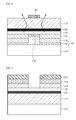
- FIGS. 2 to 6 are cross-sectional views illustrating a method of manufacturing a light emitting device according to a first embodiment of the present invention
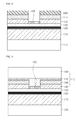
- FIGS. 7 to 10 are cross-sectional views illustrating a method of manufacturing a light emitting device according to a second embodiment of the present invention.
- FIG. 11 is a cross-sectional view of an LED package including an LED according to an embodiment of the present invention.
- FIG. 12 is a perspective view of a lighting unit according to an embodiment of the present invention.
- FIG. 13 is an exploded perspective view of a backlight unit according to an embodiment of the present invention.
- a layer when a layer (or film) is referred to as being 'on' another layer or substrate, it can be directly on another layer or substrate, or intervening layers may also be present. Further, when a layer is referred to as being 'under' another layer, it can be directly under another layer, and one or more intervening layers may also be present. In addition, when a layer is referred to as being 'between' two layers, it can be the only layer between the two layers, or one or more intervening layers may also be present.
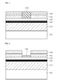
- FIG. 1 is a cross-sectional view of a light emitting device (LED) 100 according to an embodiment of the present invention.
- the light emitting device 100 includes a second conductive type semiconductor layer 130, an active layer 120, a first conductive type semiconductor layer 110, an ohmic layer 142 disposed in a first region on the second conductive type semiconductor layer 130, a reflective layer 144, a current blocking layer 150 disposed in a second region except for the first region on the second conductive type semiconductor layer 130, and a first electrode 160 disposed on the first conductive type semiconductor layer 110.
- the light emitting device 100 also includes an adhesive layer 146 disposed on the reflective layer 144 and the current blocking layer 150, a substrate 148, and a first electrode 160 on the first semiconductor layer 110.
- a second electrode 140 can include the ohmic layer 142, the reflective layer 144, the adhesive layer 146, and the substrate 148.
- the second electrode layer 140 can also include at least one of the ohmic layer 142, the reflective layer 144, the adhesive layer 146, and the second substrate 148.
- the second electrode layer 140 may include only both the ohmic layer 142 and the reflective layer 144.
- a process of forming the current blocking layer 150 is separated from a heat treating process of the ohmic layer 142 and the reflective layer 144 to form a current blocking layer that is not affected by the heat treating process and material diffusion of the reflective layer 144, thus providing a light emitting device having a high light emitting efficiency.
- the current blocking layer 150 is formed, which uses a Schottky contact through a non-ohmic metal to prevent a current from flowing into the second conductive type semiconductor layer 130 below the region of the first electrode 160.
- the current blocking layer is not affected by the heat treating process for forming the ohmic layer and the diffusion of the material of the reflective layer, the light emitting device has a high light emitting efficiency.
- the ohmic layer 142 and the reflective layer 144 that deform the current blocking layer 150 are separated from the current blocking layer 150 to dispose the ohmic layer 142 and the reflective layer 144 out of the region that is disposed under the region of the first electrode 160 on the current blocking layer 150.
- the current blocking layer 150 is also formed of a metal than can form a Schottky contact with the second conductive type semiconductor layer 130.
- the current blocking layer 150 may be formed of at least one of titanium (Ti), zirconium (Zr), chrome (Cr), gold (Au), tungsten (W), and/or an alloy including at least one of titanium (Ti), zirconium (Zr), chrome (Cr), gold (Au), and/or tungsten (W).
- the current blocking layer 150 may also vertically overlap the first electrode 160. Further, the ohmic layer 142 is in ohmic contact with the second conductive type semiconductor layer 130 in the region out of the current blocking layer 150. Thus, as depicted by dashed lines of FIG. 1 , current flowing from the second electrode layer 140 to the first electrode 160 substantially does not flow through the region where the current blocking layer 150 is disposed, but principally flows from the region out of the current blocking layer 150 to the first electrode 160.
- a current is substantially not injected to the lower side of the region of the first electrode 160 to suppress the generation of light from the active layer 120 under the first electrode 160, thus preventing heat from being generating from the device by the absorption of light generated under the first electrode 160.
- the current blocking layer 150 having Schottky barrier characteristics vertically overlaps the first electrode 160, a current flowing from the second electrode layer 140 to the first electrode 160 is prevented from intensively flowing to the lower side of the first electrode 160, and flows through the wide regions of the second conductive type semiconductor layer 130, the active layer 120, and the first conductive type semiconductor layer 110.
- the light emitting device can be driven at a stable operation voltage.
- a current intensively flows to the lower side of the first electrode 160, light is principally generated from the active layer 120 at the lower side of the first electrode 160. In this instance, the possibility that light generated from the lower side of the first electrode 160 is absorbed by the first electrode 160 to reduce light intensity or disappears in the light emitting device is high.
- the possibility that light generated from the region of the active layer 120, which does not vertically overlap the first electrode 160, is absorbed by the first electrode 160 to reduce the light intensity or disappears in the light emitting device is low.
- the optical efficiency of the light emitting device according to the current embodiment is increased.
- an un-doped GaN layer, the first conductive type semiconductor layer 110, the active layer 120, and the second conductive type semiconductor layer 130 are formed on a first substrate 105.
- a buffer layer may also be formed between the first substrate 105 and the un-doped GaN layer.
- the first substrate 105 may also be formed of at least one of sapphire (Al 2 O 3 ), Si, SiC, GaAs, ZnO, and/or MgO.
- the buffer layer may be formed as a multi-layer having a stacked structure such as AllnN/GaN, InxGa 1-x N/GaN, and Al x lnyGa 1-x-y N/In x Ga 1-x N/GaN.
- the buffer layer may be grown by injecting trimethylgallium (TMGa), trimethylindium (TMIn), trimethylalluminum (TMAI), hydrogen gas, and ammonia gas into a chamber.
- the un-doped GaN layer may also be grown by injecting trimethylgallium (TMGa), hydrogen gas, and ammonia gas into the chamber.
- the first conductive type semiconductor layer 110 may be a nitride semiconductor layer to which first conductive type semiconductor ions are implanted, for example, and may be a semiconductor layer into which N type impurity ions are implanted.
- the first conductive type semiconductor layer 110 may also be grown by injecting trimethylgallium (TMGa), silane (SiN 4 ) gas including an N type impurity (e.g., Si), hydrogen gas, and ammonia gas into the chamber.
- the active layer 120 and the second conductive type semiconductor layer 130 are formed on the first conductive type semiconductor layer 110.
- the active layer 120 may be formed in at least one of a single quantum well structure, a multi quantum well (MQW) structure, a quantum-wire structure, and a quantum dot structure.
- MQW multi quantum well
- TMGa trimethylgallium
- NH 3 ammonia
- N 2 nitrogen
- TMIn trimethylindium
- the active layer 120 may also be formed of at least one of InGaN/GaN, InGaN/InGaN, AIGaN/GaN, InAlGaN/GaN, GaAs,/AlGaAs(InGaAs), and GaP/AlGaP(InGaP).
- the second conductive type semiconductor layer 130 may be a nitride semiconductor layer to which second conductive type semiconductor ions are implanted, for example, may be a semiconductor layer into which P type impurity ions are implanted.
- the second conductive type semiconductor layer 130 may also be grown by injecting trimethylgallium (TMGa), bis-ethyl-cyclopentadienyl-magnesium (EtCp 2 Mg) ⁇ Mg(C 2 H 5 C 5 H 4 ) 2 ⁇ including a P type impurity (e.g., Mg), hydrogen gas, and ammonia gas into the chamber.
- TMGa trimethylgallium
- EtCp 2 Mg bis-ethyl-cyclopentadienyl-magnesium
- Mg P type impurity
- hydrogen gas e.g., hydrogen gas
- ammonia gas ammonia gas
- a first pattern 210 is formed in the second region on the second conductive type semiconductor layer 130.
- the first pattern 210 is used to selectively form the current blocking layer 150 on the second conductive type semiconductor layer 130.
- the first pattern 210 may also be formed as a layer such as a dielectric or a photosensitive layer.
- the ohmic layer 142 is formed in the first region on the second conductive type semiconductor layer 130.
- the first region may be a portion of the upper surface of the second conductive type semiconductor layer 130 except for the second region provided with the first pattern 210.
- the ohmic layer 142 may be formed by stacking a material such as a single metal, a metal alloy, or a metal oxide in multi layers to effectively inject holes.
- the ohmic layer 142 may include at least one of ITO, IZO(In-ZnO), GZO(Ga-ZnO), AZO(AI-ZnO), AGZO(Al-Ga ZnO), IGZO(In-Ga ZnO), IrOx, RuOx, RuOx/ITO, Ni/IrOx/Au, Ni/IrOx/Au/ITO, Ni, Pt, Cr, Ti, and ⁇ or Ag, but the present disclosure is not limited thereto.
- the ohmic layer 142 is lower than the first pattern 210, but the present disclosure is not limited thereto.
- the reflective layer 144 is formed on the ohmic layer 142.
- the reflective layer 144 may be formed as a metal layer including Al, Ag, or APC alloy (alloy including Ag, Pd, and Cu).
- a material such as aluminum or silver effectively reflects light generated from an active layer to significantly improve extraction efficiency of a light emitting device.
- the reflective layer 144 has the same level as that of the first pattern 210, but is not limited thereto.
- the first pattern 210 is removed to expose the second region, and the current blocking layer 150 is formed on the second conductive type semiconductor layer 130 in the exposed second region.
- the current blocking layer 150 may also be formed of a non-ohmic metal.
- the current blocking layer 150 may be formed of at least one of titanium (Ti), zirconium (Zr), chrome (Cr), gold (Au), and/or tungsten (W) as a metal in Schottky contact with the second conductive type semiconductor layer 130 in the exposed second region.
- the current blocking layer 150 may also include various metals including a non-ohmic metal with aluminum (AI) on the second conductive type semiconductor layer 130.
- the process of forming the current blocking layer is separated from a heat treating process of the ohmic layer and the reflective layer to form a current blocking layer that is not affected by the heat treating process and material diffusion of the reflective layer, thus providing a light emitting device having high light emitting efficiency.
- the adhesive layer 146 is formed on the reflective layer 144 and the current blocking layer 150, but the forming of the adhesive layer 146 is not always needed. That is, the reflective layer 144 may function as an adhesive layer, and the forming of the adhesive layer 146 may be removed.
- the second substrate 148 is formed on the adhesive layer 146. Then, when the first conductive type semiconductor layer 110 has a sufficient thickness of about 50 ⁇ m or greater, the forming of the second substrate 148 is removed.
- the second substrate 148 may be formed of one of a metal, a metal alloy, and ⁇ or a conductive semiconductor material, which have high electrical conductivity, to efficiently inject holes to the second substrate 148.
- the second substrate 148 may be formed of copper (Cu), copper alloy (CuAlloy), Si, Mo, or SiGe.
- a method of forming the second substrate 148 may also be an electrochemical metal deposition method or a bonding method using eutectic metal.
- the first substrate 105 is removed to expose the first conductive type semiconductor layer 110.
- a high power laser or a chemical etching method may be used to remove the first substrate 105.
- the first substrate 105 may be physically ground to remove the first substrate 105.
- the un-doped GaN layer and the buffer layer may be removed if they are present.
- the first electrode 160 is then formed on the first conductive type semiconductor layer 110.
- the first electrode 160 may be formed of at least one of titanium (Ti), chrome (Cr), nickel (Ni), aluminum (Al), platinum (Pt), and ⁇ or gold (Au).
- the first electrode 160 is formed on the first conductive type semiconductor layer 110, and may have at least one portion that vertically overlapping the current blocking layer 150. Accordingly, a current flowing to the first electrode 160 substantially does not flow through the region where the current blocking layer 150 is disposed, and flows through the region out of the current blocking layer 150.
- a current is substantially not injected to the lower side of the region of the first electrode 160 to suppress the generation of light from the active layer 120 under the first electrode 160, thus preventing heat from being generated from the device by the absorption of light generated under the first electrode 160.
- the second embodiment may adopt some of the technical features of the first embodiment, and thus the differences between the embodiments will be principally described.
- an un-doped GaN layer, the first conductive type semiconductor layer 110, the active layer 120, and the second conductive type semiconductor layer 130 are formed on the first substrate 105.
- a buffer layer may also be formed between the first substrate 105 and the un-doped GaN layer.
- the ohmic layer 142 and the reflective layer 144 are formed on the second conductive type semiconductor layer 130.
- a second pattern 220 is then formed on the first region of the reflective layer 144.
- the second pattern 220 may be formed as a layer such as a dielectric or a photosensitive layer. Thereafter, the ohmic layer 142 and the reflective layer 144 in the second region are removed using the second pattern 220 as a mask, so as to partially expose the second conductive type semiconductor layer 130.
- the second region may also vertically correspond to the region where the first electrode 160 will be formed later.
- the current blocking layer 150 is formed on the second conductive type semiconductor layer 130 exposed in the second region.
- the current blocking layer 150 may be formed of at least one of titanium (Ti), zirconium (Zr), chrome (Cr), gold (Au), and/or tungsten (W) as a metal in Schottky contact with the second conductive type semiconductor layer 130 in the exposed second region.
- the process of forming the current blocking layer is separated from a heat treating process of the ohmic layer and the reflective layer to form a current blocking layer that is not affected by the heat treating process and material diffusion of the reflective layer, thus providing a light emitting device having high light emitting efficiency.
- the second pattern 220 is removed, and the adhesive layer 146 may be formed on the reflective layer 144 and the current blocking layer 150. Thereafter, the second substrate 148 is formed on the adhesive layer 146.
- the first substrate 105 and the un-doped GaN layer are removed to expose the first conductive type semiconductor layer 110. The buffer layer is also removed if it is present. Thereafter, the first electrode 160 is formed on the first conductive type semiconductor layer 110. The first electrode 160 may have at least one portion that vertically overlapping the current blocking layer 150.
- a current is substantially not injected to the lower side of the region of the first electrode 160 to suppress the generation of light from the active layer 120 under the first electrode 160, thus preventing heat from being generated from a device by the absorption of light generated under the first electrode 160.
- the process of forming the current blocking layer is separated from a heat treating process of the ohmic layer and the reflective layer to form a current blocking layer that is not affected by the heat treating process and material diffusion of the reflective layer, thus providing a light emitting device having high light emitting efficiency.
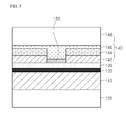
- FIG. 11 is a cross-sectional view of an LED package 200 including the LED 100 according to an embodiment of the present invention.
- the LED package 200 includes a body 205, a third electrode layer 211 and a fourth electrode layer 212 disposed in the body 205, the LED 100 disposed in the body 205 and electrically connected to the third electrode layer 211 and the fourth electrode layer 212, and a molding member 240 surrounding the LED 100.
- the body 205 may be formed of a silicon material, a synthetic resin material, or a metal material.
- An inclined surface may also be disposed around the LED 100.
- the third electrode layer 211 and the fourth electrode layer 212 are electrically separated from each other and supply a power to the LED 100. Also, the third electrode layer 211 and the fourth electrode layer 212 reflect light generated in the LED 100 to improve light efficiency in the package.
- the third electrode layer 211 and the fourth electrode layer 212 release heat generated in the LED 100 to the outside.
- the vertical type LED illustrated in FIG. 1 may be applicable as the LED 100, but is not limited thereto.
- a lateral type LED may be applicable as the LED 100.
- the LED 100 may be disposed on the body 205 or on the third electrode layer 211 or the fourth electrode layer 212.
- the LED 100 may also be electrically connected to the third electrode layer 211 and/or the fourth electrode layer 212 through a wire 230.
- the vertical type LED 100 is explained as an example, and one wire 230 may be used as an example, but is not limited thereto.
- the molding member 240 also surrounds the LED 100 to protect the LED 100. Also, a phosphor may be contained in the molding member 240 to vary a wavelength of light emitted from the LED 100.
- the LED package according to an embodiment may be applicable to a lighting system.
- the lighting system may include a lighting unit illustrated in FIG. 12 and a backlight unit illustrated in FIG. 13 .
- the lighting system may include traffic lights, a vehicle headlight, and a sign.
- FIG. 12 is a perspective view of a lighting unit 1100 according to an embodiment of the present invention.
- the lighting unit 1100 includes a case body 1110, a light emitting module 1130 disposed in the case body 1110, and a connection terminal 1120 disposed in the case body 1110 to receive a power from an external power source.
- the case body 1110 may be formed of a material having an improved heat dissipation characteristic.
- the case body 1110 may be formed of a metal material or resin material.
- the light emitting module 1130 includes a substrate 1132 and at least one light emitting device package 200 mounted on the substrate 1132.
- a circuit pattern may also be printed on an insulation material to form the substrate 1132.
- the substrate 1132 may include a printed circuit board (PCB), a metal core PCB, a flexible PCB, or a ceramic PCB.
- the substrate 1132 may be formed of a material that can effectively reflect light.
- a surface of the substrate 1132 may also be coated with a colored material, e.g., a white or silver-colored material by which light is effectively reflected.
- the light emitting device package 200 may be mounted on the substrate 1132 and include at least one light emitting diode 100.
- the light emitting diode 100 may also include a colored light emitting diode that emits red, green, blue, or white light, and an UV light emitting diode that emits ultraviolet (UV) light.
- the light emitting module 1130 may include a plurality of light emitting device packages 200 to obtain various colors and brightness.
- a white LED, a red LED, and a green LED may be disposed in combination with each other to secure a high color rendering index (CRI).
- CRI color rendering index
- connection terminal 1120 may also be electrically connected to the light emitting module 1130 to supply a power. As shown in FIG. 12 , although the connection terminal 1120 is screw-inserted into an external power source in a socket manner, the present disclosure is not limited thereto.
- the connection terminal 1120 may have a pin shape. Thus, the connection terminal 1120 may be inserted into the external power source or connected to the external power source using an interconnection.
- FIG. 13 is an exploded perspective view of a backlight unit 1200 according to an embodiment of the present invention.
- the backlight unit 1200 includes a light guide plate 1210, a light emitting module 1240, a reflective member 1220, and a bottom cover 1230, but is not limited thereto.
- the light emitting module 1240 also provides light to the light guide plate 1210.
- the reflective member 1220 may be disposed below the light guide plate 1210.
- the bottom cover 1230 may also receive the light guide plate 1210, the light emitting module 1240, and the reflective member 1220.
- the light guide plate 1210 diffuses light to produce planar light.
- the light guide plate 1210 may be formed of a transparent material.
- the light guide plate 1210 may be formed of one of an acrylic resin-based material such as polymethylmethacrylate (PMMA), a polyethylene terephthalate (PET) resin, a poly carbonate (PC) resin, a cyclic olefin copolymer (COC) resin, and/or a polyethylene naphthalate (PEN) resin.
- PMMA polymethylmethacrylate
- PET polyethylene terephthalate
- PC poly carbonate
- COC cyclic olefin copolymer
- PEN polyethylene naphthalate
- the light emitting module 1240 provides light to at least one surface of the light guide plate 1210.
- the light emitting module 1240 may be used as a light source of a display device including the backlight unit.
- the light emitting module 1240 may also contact the light guide plate 1210, but is not limited thereto.
- the light emitting module 1240 includes a substrate 1242 and a plurality of light emitting device packages 200 mounted on the substrate 1242.
- the substrate 1242 may also contact the light guide plate 1210, but is not limited thereto.
- the substrate 1242 may be a PCB including a circuit pattern.
- the substrate 1242 may include a metal core PCB or a flexible PCB as well as the PCB, but is not limited thereto.
- a light emitting surface of each of the plurality of light emitting device packages 200 may be spaced a predetermined distance from the light guide plate 1210.
- the reflective member 1220 may be disposed below the light guide plate 1210.
- the reflective member 1220 also reflects light incident onto a bottom surface of the light guide plate 1210 to proceed in an upward direction, thereby improving brightness of the backlight unit.
- the reflective member may be formed of one of PET, PC, and PVC, but is not limited thereto.
- the bottom cover 1230 may receive the light guide plate 1210, the light emitting module 1240, and the reflective member 1220.
- the bottom cover 1230 may have a box shape with an open upper side, but is not limited thereto.
- the bottom cover 1230 may also be formed of a metal material or a resin material.
- the bottom cover 1230 may be manufactured using a press forming process or an extrusion molding process.
- the current blocking layer includes metal rather than a dielectric or a non-ohmic metal to block a current. Further, the current blocking layer is not transformed into a layer to which a current can be injected through a heat treating process to form an ohmic layer.
- any reference in this specification to "one embodiment,” “an embodiment,” “example embodiment,” etc. means that a particular feature, structure, or characteristic described in connection with the embodiment is included in at least one embodiment of the invention.
- the appearances of such phrases in various places in the specification are not necessarily all referring to the same embodiment.
Landscapes
- Led Devices (AREA)
- Engineering & Computer Science (AREA)
- Microelectronics & Electronic Packaging (AREA)
Applications Claiming Priority (1)
| Application Number | Priority Date | Filing Date | Title |
|---|---|---|---|
| KR20090039015A KR100999726B1 (ko) | 2009-05-04 | 2009-05-04 | 발광소자 및 그 제조방법 |
Publications (3)
| Publication Number | Publication Date |
|---|---|
| EP2249405A2 true EP2249405A2 (de) | 2010-11-10 |
| EP2249405A3 EP2249405A3 (de) | 2014-01-08 |
| EP2249405B1 EP2249405B1 (de) | 2018-04-25 |
Family
ID=42459435
Family Applications (1)
| Application Number | Title | Priority Date | Filing Date |
|---|---|---|---|
| EP10161793.4A Active EP2249405B1 (de) | 2009-05-04 | 2010-05-03 | Verfahren zur Herstellung einer lichtemittierenden Vorrichtung |
Country Status (4)
| Country | Link |
|---|---|
| US (4) | US8222661B2 (de) |
| EP (1) | EP2249405B1 (de) |
| KR (1) | KR100999726B1 (de) |
| CN (1) | CN101882658B (de) |
Cited By (3)
| Publication number | Priority date | Publication date | Assignee | Title |
|---|---|---|---|---|
| WO2013068878A1 (en) * | 2011-11-07 | 2013-05-16 | Koninklijke Philips Electronics N.V. | Improved p-contact with more uniform injection and lower optical loss |
| EP2365541A3 (de) * | 2010-03-10 | 2015-08-19 | LG Innotek Co., Ltd. | Lichtemittierende Vorrichtung, Herstellungsverfahren für die lichtemittierende Vorrichtung, Gehäuse für lichtemittierende Vorrichtung und Beleuchtungseinheit |
| WO2016165983A1 (en) * | 2015-04-15 | 2016-10-20 | Koninklijke Philips N.V. | Light emitting device with reflector and a top contact |
Families Citing this family (11)
| Publication number | Priority date | Publication date | Assignee | Title |
|---|---|---|---|---|
| KR100999726B1 (ko) * | 2009-05-04 | 2010-12-08 | 엘지이노텍 주식회사 | 발광소자 및 그 제조방법 |
| JP2011249510A (ja) * | 2010-05-26 | 2011-12-08 | Toshiba Corp | 発光素子 |
| KR101734558B1 (ko) * | 2011-02-28 | 2017-05-11 | 엘지이노텍 주식회사 | 발광 소자 |
| US20130001510A1 (en) * | 2011-06-29 | 2013-01-03 | SemiLEDs Optoelectronics Co., Ltd. | Optoelectronic device having current blocking insulation layer for uniform temperature distribution and method of fabrication |
| KR101954202B1 (ko) * | 2012-06-11 | 2019-03-05 | 엘지이노텍 주식회사 | 발광소자 및 이를 포함하는 조명시스템 |
| CN102709421B (zh) * | 2012-06-21 | 2014-11-05 | 安徽三安光电有限公司 | 一种具有双反射层的氮化镓基发光二极管 |
| CN104617191A (zh) * | 2015-01-14 | 2015-05-13 | 映瑞光电科技(上海)有限公司 | 一种具有电流阻挡结构的led垂直芯片及其制备方法 |
| JP6468459B2 (ja) * | 2015-03-31 | 2019-02-13 | ウシオ電機株式会社 | 半導体発光素子 |
| CN107256871B (zh) * | 2017-06-27 | 2019-09-27 | 上海天马微电子有限公司 | 微发光二极管显示面板和显示装置 |
| CN116825925A (zh) * | 2018-12-24 | 2023-09-29 | 泉州三安半导体科技有限公司 | 一种发光二极管及其制作方法 |
| CN111261762A (zh) * | 2020-03-20 | 2020-06-09 | 西安唐晶量子科技有限公司 | 一种具有电流阻挡层的氮化镓基垂直结构发光二极管及其制作方法 |
Family Cites Families (25)
| Publication number | Priority date | Publication date | Assignee | Title |
|---|---|---|---|---|
| JP2001144321A (ja) | 1999-11-04 | 2001-05-25 | Shurai Kagi Kofun Yugenkoshi | 発光素子及びその製造方法 |
| US6492661B1 (en) * | 1999-11-04 | 2002-12-10 | Fen-Ren Chien | Light emitting semiconductor device having reflection layer structure |
| JP2002151733A (ja) | 2000-11-15 | 2002-05-24 | Hitachi Cable Ltd | 発光ダイオードおよびその製造方法 |
| JP2003046119A (ja) | 2001-07-26 | 2003-02-14 | Hitachi Cable Ltd | 発光ダイオード及びその製造方法 |
| TWI278995B (en) | 2002-01-28 | 2007-04-11 | Nichia Corp | Nitride semiconductor element with a supporting substrate and a method for producing a nitride semiconductor element |
| US7041529B2 (en) * | 2002-10-23 | 2006-05-09 | Shin-Etsu Handotai Co., Ltd. | Light-emitting device and method of fabricating the same |
| TW578318B (en) * | 2002-12-31 | 2004-03-01 | United Epitaxy Co Ltd | Light emitting diode and method of making the same |
| EP1709694B1 (de) | 2004-01-26 | 2017-03-15 | OSRAM Opto Semiconductors GmbH | Dünnfilm-led mit einer stromaufweitungsstruktur |
| US7795623B2 (en) * | 2004-06-30 | 2010-09-14 | Cree, Inc. | Light emitting devices having current reducing structures and methods of forming light emitting devices having current reducing structures |
| TWI247441B (en) | 2005-01-21 | 2006-01-11 | United Epitaxy Co Ltd | Light emitting diode and fabricating method thereof |
| CN100388515C (zh) * | 2005-09-30 | 2008-05-14 | 晶能光电(江西)有限公司 | 半导体发光器件及其制造方法 |
| KR100721147B1 (ko) | 2005-11-23 | 2007-05-22 | 삼성전기주식회사 | 수직구조 질화갈륨계 발광다이오드 소자 |
| KR100752696B1 (ko) | 2006-02-16 | 2007-08-29 | 삼성전기주식회사 | 수직구조 질화갈륨계 발광다이오드 소자 |
| JP4946195B2 (ja) | 2006-06-19 | 2012-06-06 | サンケン電気株式会社 | 半導体発光素子及びその製造方法 |
| KR100856089B1 (ko) * | 2006-08-23 | 2008-09-02 | 삼성전기주식회사 | 수직구조 질화갈륨계 발광 다이오드 소자 및 그 제조방법 |
| JP2008053685A (ja) | 2006-08-23 | 2008-03-06 | Samsung Electro Mech Co Ltd | 垂直構造窒化ガリウム系発光ダイオード素子及びその製造方法 |
| JP2008103534A (ja) * | 2006-10-19 | 2008-05-01 | Hitachi Cable Ltd | 半導体発光素子 |
| JP4985067B2 (ja) | 2007-04-11 | 2012-07-25 | 日立電線株式会社 | 半導体発光素子 |
| JP5346443B2 (ja) | 2007-04-16 | 2013-11-20 | ローム株式会社 | 半導体発光素子およびその製造方法 |
| US7759670B2 (en) * | 2007-06-12 | 2010-07-20 | SemiLEDs Optoelectronics Co., Ltd. | Vertical LED with current guiding structure |
| KR20090027329A (ko) | 2007-09-12 | 2009-03-17 | 삼성전기주식회사 | 수직구조 반도체 발광소자 및 그 제조 방법 |
| KR101438818B1 (ko) * | 2008-04-01 | 2014-09-05 | 엘지이노텍 주식회사 | 발광다이오드 소자 |
| CN102047454B (zh) * | 2008-04-16 | 2013-04-10 | Lg伊诺特有限公司 | 发光器件及其制造方法 |
| JP5057398B2 (ja) | 2008-08-05 | 2012-10-24 | シャープ株式会社 | 窒化物半導体発光素子およびその製造方法 |
| KR100999726B1 (ko) * | 2009-05-04 | 2010-12-08 | 엘지이노텍 주식회사 | 발광소자 및 그 제조방법 |
-
2009
- 2009-05-04 KR KR20090039015A patent/KR100999726B1/ko not_active Expired - Fee Related
-
2010
- 2010-05-03 US US12/772,985 patent/US8222661B2/en not_active Expired - Fee Related
- 2010-05-03 EP EP10161793.4A patent/EP2249405B1/de active Active
- 2010-05-04 CN CN201010170274.7A patent/CN101882658B/zh active Active
-
2012
- 2012-06-18 US US13/526,411 patent/US8513681B2/en active Active
-
2013
- 2013-08-09 US US13/963,877 patent/US8907363B2/en active Active
-
2014
- 2014-11-06 US US14/535,122 patent/US9343640B2/en active Active
Non-Patent Citations (1)
| Title |
|---|
| None |
Cited By (6)
| Publication number | Priority date | Publication date | Assignee | Title |
|---|---|---|---|---|
| EP2365541A3 (de) * | 2010-03-10 | 2015-08-19 | LG Innotek Co., Ltd. | Lichtemittierende Vorrichtung, Herstellungsverfahren für die lichtemittierende Vorrichtung, Gehäuse für lichtemittierende Vorrichtung und Beleuchtungseinheit |
| WO2013068878A1 (en) * | 2011-11-07 | 2013-05-16 | Koninklijke Philips Electronics N.V. | Improved p-contact with more uniform injection and lower optical loss |
| US9312437B2 (en) | 2011-11-07 | 2016-04-12 | Koninklijke Philips N.V. | P-contact with more uniform injection and lower optical loss |
| US9583679B2 (en) | 2011-11-07 | 2017-02-28 | Koninklijke Philips N.V. | P-contact with more uniform injection and lower optical loss |
| WO2016165983A1 (en) * | 2015-04-15 | 2016-10-20 | Koninklijke Philips N.V. | Light emitting device with reflector and a top contact |
| US10026881B2 (en) | 2015-04-15 | 2018-07-17 | Koninklijke Philips N.V. | Light emitting device with reflector and a top contact |
Also Published As
| Publication number | Publication date |
|---|---|
| US9343640B2 (en) | 2016-05-17 |
| CN101882658B (zh) | 2014-11-19 |
| US20100276715A1 (en) | 2010-11-04 |
| KR20100120027A (ko) | 2010-11-12 |
| US20120256226A1 (en) | 2012-10-11 |
| EP2249405B1 (de) | 2018-04-25 |
| KR100999726B1 (ko) | 2010-12-08 |
| EP2249405A3 (de) | 2014-01-08 |
| US8513681B2 (en) | 2013-08-20 |
| US20150060927A1 (en) | 2015-03-05 |
| US8907363B2 (en) | 2014-12-09 |
| CN101882658A (zh) | 2010-11-10 |
| US8222661B2 (en) | 2012-07-17 |
| US20130328092A1 (en) | 2013-12-12 |
Similar Documents
| Publication | Publication Date | Title |
|---|---|---|
| EP2249405B1 (de) | Verfahren zur Herstellung einer lichtemittierenden Vorrichtung | |
| US8324649B2 (en) | Light emitting device | |
| EP2226856B1 (de) | Lichtemittierende Vorrichtung | |
| EP2246891B1 (de) | Lichtemittierende Vorrichtung, Gehäuse für lichtemittierende Vorrichtung und Beleuchtungssystem damit | |
| JP2011139066A (ja) | 発光素子、発光素子パッケージおよび照明システム | |
| CN101847676B (zh) | 发光器件、发光器件封装和包括发光器件封装的照明系统 | |
| US8421106B2 (en) | Light emitting device, system and package | |
| US8809884B2 (en) | Light emitting device including an electrode on a textured surface, light emitting device package and lighting system | |
| US9444016B2 (en) | Light emitting device | |
| US20150255675A1 (en) | Light-emitting device | |
| KR101829798B1 (ko) | 발광소자 | |
| KR102057715B1 (ko) | 발광소자 | |
| KR101856213B1 (ko) | 발광소자 및 그 제조방법 | |
| KR20110120080A (ko) | 발광소자, 발광소자의 제조방법, 발광소자 패키지 및 조명시스템 | |
| KR20120011176A (ko) | 발광소자 | |
| KR20130019277A (ko) | 발광소자 | |
| KR20130073349A (ko) | 발광 소자 |
Legal Events
| Date | Code | Title | Description |
|---|---|---|---|
| PUAI | Public reference made under article 153(3) epc to a published international application that has entered the european phase |
Free format text: ORIGINAL CODE: 0009012 |
|
| 17P | Request for examination filed |
Effective date: 20100503 |
|
| AK | Designated contracting states |
Kind code of ref document: A2 Designated state(s): AL AT BE BG CH CY CZ DE DK EE ES FI FR GB GR HR HU IE IS IT LI LT LU LV MC MK MT NL NO PL PT RO SE SI SK SM TR |
|
| AX | Request for extension of the european patent |
Extension state: BA ME RS |
|
| PUAL | Search report despatched |
Free format text: ORIGINAL CODE: 0009013 |
|
| AK | Designated contracting states |
Kind code of ref document: A3 Designated state(s): AL AT BE BG CH CY CZ DE DK EE ES FI FR GB GR HR HU IE IS IT LI LT LU LV MC MK MT NL NO PL PT RO SE SI SK SM TR |
|
| AX | Request for extension of the european patent |
Extension state: BA ME RS |
|
| RIC1 | Information provided on ipc code assigned before grant |
Ipc: H01L 33/42 20100101ALN20131202BHEP Ipc: H01L 33/40 20100101ALN20131202BHEP Ipc: H01L 33/14 20100101AFI20131202BHEP Ipc: H01L 33/38 20100101ALN20131202BHEP |
|
| RAP1 | Party data changed (applicant data changed or rights of an application transferred) |
Owner name: LG INNOTEK CO., LTD. |
|
| RBV | Designated contracting states (corrected) |
Designated state(s): AL AT BE BG CH CY CZ DE DK EE ES FI FR GB GR HR HU IE IS IT LI LT LU LV MC MK MT NL NO PL PT RO SE SI SK SM TR |
|
| 17Q | First examination report despatched |
Effective date: 20150818 |
|
| RAP1 | Party data changed (applicant data changed or rights of an application transferred) |
Owner name: LG INNOTEK CO., LTD. |
|
| REG | Reference to a national code |
Ref country code: DE Ref legal event code: R079 Ref document number: 602010050133 Country of ref document: DE Free format text: PREVIOUS MAIN CLASS: H01L0033140000 Ipc: H01L0033000000 |
|
| GRAP | Despatch of communication of intention to grant a patent |
Free format text: ORIGINAL CODE: EPIDOSNIGR1 |
|
| STAA | Information on the status of an ep patent application or granted ep patent |
Free format text: STATUS: GRANT OF PATENT IS INTENDED |
|
| RIC1 | Information provided on ipc code assigned before grant |
Ipc: H01L 33/00 20100101AFI20171019BHEP Ipc: H01L 33/14 20100101ALI20171019BHEP Ipc: H01L 33/42 20100101ALN20171019BHEP Ipc: H01L 33/38 20100101ALN20171019BHEP Ipc: H01L 33/40 20100101ALN20171019BHEP |
|
| INTG | Intention to grant announced |
Effective date: 20171107 |
|
| GRAA | (expected) grant |
Free format text: ORIGINAL CODE: 0009210 |
|
| GRAS | Grant fee paid |
Free format text: ORIGINAL CODE: EPIDOSNIGR3 |
|
| STAA | Information on the status of an ep patent application or granted ep patent |
Free format text: STATUS: THE PATENT HAS BEEN GRANTED |
|
| AK | Designated contracting states |
Kind code of ref document: B1 Designated state(s): AL AT BE BG CH CY CZ DE DK EE ES FI FR GB GR HR HU IE IS IT LI LT LU LV MC MK MT NL NO PL PT RO SE SI SK SM TR |
|
| REG | Reference to a national code |
Ref country code: GB Ref legal event code: FG4D |
|
| REG | Reference to a national code |
Ref country code: CH Ref legal event code: EP |
|
| REG | Reference to a national code |
Ref country code: FR Ref legal event code: PLFP Year of fee payment: 9 |
|
| REG | Reference to a national code |
Ref country code: AT Ref legal event code: REF Ref document number: 993754 Country of ref document: AT Kind code of ref document: T Effective date: 20180515 |
|
| REG | Reference to a national code |
Ref country code: IE Ref legal event code: FG4D |
|
| REG | Reference to a national code |
Ref country code: DE Ref legal event code: R096 Ref document number: 602010050133 Country of ref document: DE |
|
| REG | Reference to a national code |
Ref country code: NL Ref legal event code: MP Effective date: 20180425 |
|
| REG | Reference to a national code |
Ref country code: LT Ref legal event code: MG4D |
|
| PG25 | Lapsed in a contracting state [announced via postgrant information from national office to epo] |
Ref country code: NL Free format text: LAPSE BECAUSE OF FAILURE TO SUBMIT A TRANSLATION OF THE DESCRIPTION OR TO PAY THE FEE WITHIN THE PRESCRIBED TIME-LIMIT Effective date: 20180425 |
|
| PG25 | Lapsed in a contracting state [announced via postgrant information from national office to epo] |
Ref country code: NO Free format text: LAPSE BECAUSE OF FAILURE TO SUBMIT A TRANSLATION OF THE DESCRIPTION OR TO PAY THE FEE WITHIN THE PRESCRIBED TIME-LIMIT Effective date: 20180725 Ref country code: FI Free format text: LAPSE BECAUSE OF FAILURE TO SUBMIT A TRANSLATION OF THE DESCRIPTION OR TO PAY THE FEE WITHIN THE PRESCRIBED TIME-LIMIT Effective date: 20180425 Ref country code: BG Free format text: LAPSE BECAUSE OF FAILURE TO SUBMIT A TRANSLATION OF THE DESCRIPTION OR TO PAY THE FEE WITHIN THE PRESCRIBED TIME-LIMIT Effective date: 20180725 Ref country code: LT Free format text: LAPSE BECAUSE OF FAILURE TO SUBMIT A TRANSLATION OF THE DESCRIPTION OR TO PAY THE FEE WITHIN THE PRESCRIBED TIME-LIMIT Effective date: 20180425 Ref country code: PL Free format text: LAPSE BECAUSE OF FAILURE TO SUBMIT A TRANSLATION OF THE DESCRIPTION OR TO PAY THE FEE WITHIN THE PRESCRIBED TIME-LIMIT Effective date: 20180425 Ref country code: ES Free format text: LAPSE BECAUSE OF FAILURE TO SUBMIT A TRANSLATION OF THE DESCRIPTION OR TO PAY THE FEE WITHIN THE PRESCRIBED TIME-LIMIT Effective date: 20180425 Ref country code: SE Free format text: LAPSE BECAUSE OF FAILURE TO SUBMIT A TRANSLATION OF THE DESCRIPTION OR TO PAY THE FEE WITHIN THE PRESCRIBED TIME-LIMIT Effective date: 20180425 |
|
| PG25 | Lapsed in a contracting state [announced via postgrant information from national office to epo] |
Ref country code: LV Free format text: LAPSE BECAUSE OF FAILURE TO SUBMIT A TRANSLATION OF THE DESCRIPTION OR TO PAY THE FEE WITHIN THE PRESCRIBED TIME-LIMIT Effective date: 20180425 Ref country code: GR Free format text: LAPSE BECAUSE OF FAILURE TO SUBMIT A TRANSLATION OF THE DESCRIPTION OR TO PAY THE FEE WITHIN THE PRESCRIBED TIME-LIMIT Effective date: 20180726 Ref country code: HR Free format text: LAPSE BECAUSE OF FAILURE TO SUBMIT A TRANSLATION OF THE DESCRIPTION OR TO PAY THE FEE WITHIN THE PRESCRIBED TIME-LIMIT Effective date: 20180425 |
|
| REG | Reference to a national code |
Ref country code: CH Ref legal event code: PL |
|
| REG | Reference to a national code |
Ref country code: AT Ref legal event code: MK05 Ref document number: 993754 Country of ref document: AT Kind code of ref document: T Effective date: 20180425 |
|
| PG25 | Lapsed in a contracting state [announced via postgrant information from national office to epo] |
Ref country code: PT Free format text: LAPSE BECAUSE OF FAILURE TO SUBMIT A TRANSLATION OF THE DESCRIPTION OR TO PAY THE FEE WITHIN THE PRESCRIBED TIME-LIMIT Effective date: 20180827 |
|
| REG | Reference to a national code |
Ref country code: DE Ref legal event code: R097 Ref document number: 602010050133 Country of ref document: DE |
|
| REG | Reference to a national code |
Ref country code: BE Ref legal event code: MM Effective date: 20180531 |
|
| PG25 | Lapsed in a contracting state [announced via postgrant information from national office to epo] |
Ref country code: DK Free format text: LAPSE BECAUSE OF FAILURE TO SUBMIT A TRANSLATION OF THE DESCRIPTION OR TO PAY THE FEE WITHIN THE PRESCRIBED TIME-LIMIT Effective date: 20180425 Ref country code: AT Free format text: LAPSE BECAUSE OF FAILURE TO SUBMIT A TRANSLATION OF THE DESCRIPTION OR TO PAY THE FEE WITHIN THE PRESCRIBED TIME-LIMIT Effective date: 20180425 Ref country code: EE Free format text: LAPSE BECAUSE OF FAILURE TO SUBMIT A TRANSLATION OF THE DESCRIPTION OR TO PAY THE FEE WITHIN THE PRESCRIBED TIME-LIMIT Effective date: 20180425 Ref country code: MC Free format text: LAPSE BECAUSE OF FAILURE TO SUBMIT A TRANSLATION OF THE DESCRIPTION OR TO PAY THE FEE WITHIN THE PRESCRIBED TIME-LIMIT Effective date: 20180425 Ref country code: SK Free format text: LAPSE BECAUSE OF FAILURE TO SUBMIT A TRANSLATION OF THE DESCRIPTION OR TO PAY THE FEE WITHIN THE PRESCRIBED TIME-LIMIT Effective date: 20180425 Ref country code: CZ Free format text: LAPSE BECAUSE OF FAILURE TO SUBMIT A TRANSLATION OF THE DESCRIPTION OR TO PAY THE FEE WITHIN THE PRESCRIBED TIME-LIMIT Effective date: 20180425 Ref country code: RO Free format text: LAPSE BECAUSE OF FAILURE TO SUBMIT A TRANSLATION OF THE DESCRIPTION OR TO PAY THE FEE WITHIN THE PRESCRIBED TIME-LIMIT Effective date: 20180425 |
|
| REG | Reference to a national code |
Ref country code: IE Ref legal event code: MM4A |
|
| PG25 | Lapsed in a contracting state [announced via postgrant information from national office to epo] |
Ref country code: LI Free format text: LAPSE BECAUSE OF NON-PAYMENT OF DUE FEES Effective date: 20180531 Ref country code: IT Free format text: LAPSE BECAUSE OF FAILURE TO SUBMIT A TRANSLATION OF THE DESCRIPTION OR TO PAY THE FEE WITHIN THE PRESCRIBED TIME-LIMIT Effective date: 20180425 Ref country code: SM Free format text: LAPSE BECAUSE OF FAILURE TO SUBMIT A TRANSLATION OF THE DESCRIPTION OR TO PAY THE FEE WITHIN THE PRESCRIBED TIME-LIMIT Effective date: 20180425 Ref country code: CH Free format text: LAPSE BECAUSE OF NON-PAYMENT OF DUE FEES Effective date: 20180531 |
|
| PLBE | No opposition filed within time limit |
Free format text: ORIGINAL CODE: 0009261 |
|
| STAA | Information on the status of an ep patent application or granted ep patent |
Free format text: STATUS: NO OPPOSITION FILED WITHIN TIME LIMIT |
|
| GBPC | Gb: european patent ceased through non-payment of renewal fee |
Effective date: 20180725 |
|
| PG25 | Lapsed in a contracting state [announced via postgrant information from national office to epo] |
Ref country code: LU Free format text: LAPSE BECAUSE OF NON-PAYMENT OF DUE FEES Effective date: 20180503 |
|
| 26N | No opposition filed |
Effective date: 20190128 |
|
| PG25 | Lapsed in a contracting state [announced via postgrant information from national office to epo] |
Ref country code: IE Free format text: LAPSE BECAUSE OF NON-PAYMENT OF DUE FEES Effective date: 20180503 Ref country code: GB Free format text: LAPSE BECAUSE OF NON-PAYMENT OF DUE FEES Effective date: 20180725 |
|
| PG25 | Lapsed in a contracting state [announced via postgrant information from national office to epo] |
Ref country code: BE Free format text: LAPSE BECAUSE OF NON-PAYMENT OF DUE FEES Effective date: 20180531 Ref country code: SI Free format text: LAPSE BECAUSE OF FAILURE TO SUBMIT A TRANSLATION OF THE DESCRIPTION OR TO PAY THE FEE WITHIN THE PRESCRIBED TIME-LIMIT Effective date: 20180425 |
|
| PG25 | Lapsed in a contracting state [announced via postgrant information from national office to epo] |
Ref country code: AL Free format text: LAPSE BECAUSE OF FAILURE TO SUBMIT A TRANSLATION OF THE DESCRIPTION OR TO PAY THE FEE WITHIN THE PRESCRIBED TIME-LIMIT Effective date: 20180425 |
|
| PG25 | Lapsed in a contracting state [announced via postgrant information from national office to epo] |
Ref country code: MT Free format text: LAPSE BECAUSE OF NON-PAYMENT OF DUE FEES Effective date: 20180503 |
|
| PG25 | Lapsed in a contracting state [announced via postgrant information from national office to epo] |
Ref country code: TR Free format text: LAPSE BECAUSE OF FAILURE TO SUBMIT A TRANSLATION OF THE DESCRIPTION OR TO PAY THE FEE WITHIN THE PRESCRIBED TIME-LIMIT Effective date: 20180425 |
|
| PG25 | Lapsed in a contracting state [announced via postgrant information from national office to epo] |
Ref country code: HU Free format text: LAPSE BECAUSE OF FAILURE TO SUBMIT A TRANSLATION OF THE DESCRIPTION OR TO PAY THE FEE WITHIN THE PRESCRIBED TIME-LIMIT; INVALID AB INITIO Effective date: 20100503 |
|
| PG25 | Lapsed in a contracting state [announced via postgrant information from national office to epo] |
Ref country code: MK Free format text: LAPSE BECAUSE OF NON-PAYMENT OF DUE FEES Effective date: 20180425 Ref country code: CY Free format text: LAPSE BECAUSE OF FAILURE TO SUBMIT A TRANSLATION OF THE DESCRIPTION OR TO PAY THE FEE WITHIN THE PRESCRIBED TIME-LIMIT Effective date: 20180425 |
|
| PG25 | Lapsed in a contracting state [announced via postgrant information from national office to epo] |
Ref country code: IS Free format text: LAPSE BECAUSE OF FAILURE TO SUBMIT A TRANSLATION OF THE DESCRIPTION OR TO PAY THE FEE WITHIN THE PRESCRIBED TIME-LIMIT Effective date: 20180825 |
|
| REG | Reference to a national code |
Ref country code: DE Ref legal event code: R081 Ref document number: 602010050133 Country of ref document: DE Owner name: SUZHOU LEKIN SEMICONDUCTOR CO. LTD., TAICANG, CN Free format text: FORMER OWNER: LG INNOTEK CO., LTD., SEOUL, KR |
|
| PGFP | Annual fee paid to national office [announced via postgrant information from national office to epo] |
Ref country code: FR Payment date: 20220408 Year of fee payment: 13 |
|
| PG25 | Lapsed in a contracting state [announced via postgrant information from national office to epo] |
Ref country code: FR Free format text: LAPSE BECAUSE OF NON-PAYMENT OF DUE FEES Effective date: 20230531 |
|
| REG | Reference to a national code |
Ref country code: DE Ref legal event code: R079 Ref document number: 602010050133 Country of ref document: DE Free format text: PREVIOUS MAIN CLASS: H01L0033000000 Ipc: H10H0020000000 |
|
| PGFP | Annual fee paid to national office [announced via postgrant information from national office to epo] |
Ref country code: DE Payment date: 20250408 Year of fee payment: 16 |