EP2249412A1 - Dispositif semi-conducteur organique et procédé de fabrication de celui-ci - Google Patents
Dispositif semi-conducteur organique et procédé de fabrication de celui-ci Download PDFInfo
- Publication number
- EP2249412A1 EP2249412A1 EP09159689A EP09159689A EP2249412A1 EP 2249412 A1 EP2249412 A1 EP 2249412A1 EP 09159689 A EP09159689 A EP 09159689A EP 09159689 A EP09159689 A EP 09159689A EP 2249412 A1 EP2249412 A1 EP 2249412A1
- Authority
- EP
- European Patent Office
- Prior art keywords
- electrically conductive
- layer
- insulating barrier
- conductive structure
- electrically insulating
- Prior art date
- Legal status (The legal status is an assumption and is not a legal conclusion. Google has not performed a legal analysis and makes no representation as to the accuracy of the status listed.)
- Withdrawn
Links
- 239000004065 semiconductor Substances 0.000 title claims abstract description 36
- 238000000034 method Methods 0.000 title claims description 33
- 238000004519 manufacturing process Methods 0.000 title claims description 11
- 230000004888 barrier function Effects 0.000 claims abstract description 93
- 238000005538 encapsulation Methods 0.000 claims abstract description 9
- 239000000463 material Substances 0.000 claims description 21
- 238000002347 injection Methods 0.000 claims description 17
- 239000007924 injection Substances 0.000 claims description 17
- 238000000151 deposition Methods 0.000 claims description 11
- 239000000758 substrate Substances 0.000 claims description 9
- 229910052581 Si3N4 Inorganic materials 0.000 claims description 6
- HQVNEWCFYHHQES-UHFFFAOYSA-N silicon nitride Chemical compound N12[Si]34N5[Si]62N3[Si]51N64 HQVNEWCFYHHQES-UHFFFAOYSA-N 0.000 claims description 6
- VYPSYNLAJGMNEJ-UHFFFAOYSA-N Silicium dioxide Chemical compound O=[Si]=O VYPSYNLAJGMNEJ-UHFFFAOYSA-N 0.000 claims description 5
- 229910052814 silicon oxide Inorganic materials 0.000 claims description 5
- 239000000615 nonconductor Substances 0.000 claims description 3
- 230000001590 oxidative effect Effects 0.000 claims description 2
- 238000005530 etching Methods 0.000 claims 1
- 239000010410 layer Substances 0.000 description 149
- 229910052751 metal Inorganic materials 0.000 description 15
- 239000002184 metal Substances 0.000 description 15
- 239000011888 foil Substances 0.000 description 11
- 239000011248 coating agent Substances 0.000 description 6
- 238000000576 coating method Methods 0.000 description 6
- 238000007639 printing Methods 0.000 description 6
- 238000002207 thermal evaporation Methods 0.000 description 5
- PNEYBMLMFCGWSK-UHFFFAOYSA-N Alumina Chemical group [O-2].[O-2].[O-2].[Al+3].[Al+3] PNEYBMLMFCGWSK-UHFFFAOYSA-N 0.000 description 4
- 229910052782 aluminium Inorganic materials 0.000 description 4
- XAGFODPZIPBFFR-UHFFFAOYSA-N aluminium Chemical compound [Al] XAGFODPZIPBFFR-UHFFFAOYSA-N 0.000 description 4
- QVGXLLKOCUKJST-UHFFFAOYSA-N atomic oxygen Chemical compound [O] QVGXLLKOCUKJST-UHFFFAOYSA-N 0.000 description 4
- 239000001301 oxygen Substances 0.000 description 4
- 229910052760 oxygen Inorganic materials 0.000 description 4
- 229920002120 photoresistant polymer Polymers 0.000 description 4
- 229920000642 polymer Polymers 0.000 description 4
- 229920001609 Poly(3,4-ethylenedioxythiophene) Polymers 0.000 description 3
- 238000005229 chemical vapour deposition Methods 0.000 description 3
- 150000004767 nitrides Chemical class 0.000 description 3
- 239000010409 thin film Substances 0.000 description 3
- BQCADISMDOOEFD-UHFFFAOYSA-N Silver Chemical compound [Ag] BQCADISMDOOEFD-UHFFFAOYSA-N 0.000 description 2
- 238000007743 anodising Methods 0.000 description 2
- 239000012159 carrier gas Substances 0.000 description 2
- 229920001940 conductive polymer Polymers 0.000 description 2
- 238000001704 evaporation Methods 0.000 description 2
- 230000008020 evaporation Effects 0.000 description 2
- 239000010408 film Substances 0.000 description 2
- 238000007646 gravure printing Methods 0.000 description 2
- 238000007641 inkjet printing Methods 0.000 description 2
- 238000005334 plasma enhanced chemical vapour deposition Methods 0.000 description 2
- 238000000623 plasma-assisted chemical vapour deposition Methods 0.000 description 2
- 238000010022 rotary screen printing Methods 0.000 description 2
- 238000007650 screen-printing Methods 0.000 description 2
- 229910052709 silver Inorganic materials 0.000 description 2
- 239000004332 silver Substances 0.000 description 2
- 238000007764 slot die coating Methods 0.000 description 2
- 150000003384 small molecules Chemical class 0.000 description 2
- 238000004528 spin coating Methods 0.000 description 2
- 238000004544 sputter deposition Methods 0.000 description 2
- 239000000126 substance Substances 0.000 description 2
- 239000000725 suspension Substances 0.000 description 2
- 238000001947 vapour-phase growth Methods 0.000 description 2
- GEQBRULPNIVQPP-UHFFFAOYSA-N 2-[3,5-bis(1-phenylbenzimidazol-2-yl)phenyl]-1-phenylbenzimidazole Chemical compound C1=CC=CC=C1N1C2=CC=CC=C2N=C1C1=CC(C=2N(C3=CC=CC=C3N=2)C=2C=CC=CC=2)=CC(C=2N(C3=CC=CC=C3N=2)C=2C=CC=CC=2)=C1 GEQBRULPNIVQPP-UHFFFAOYSA-N 0.000 description 1
- VQGHOUODWALEFC-UHFFFAOYSA-N 2-phenylpyridine Chemical compound C1=CC=CC=C1C1=CC=CC=N1 VQGHOUODWALEFC-UHFFFAOYSA-N 0.000 description 1
- 229910000831 Steel Inorganic materials 0.000 description 1
- -1 aluminum and silver Chemical class 0.000 description 1
- 229910010293 ceramic material Inorganic materials 0.000 description 1
- 239000002322 conducting polymer Substances 0.000 description 1
- 239000004020 conductor Substances 0.000 description 1
- 230000008021 deposition Effects 0.000 description 1
- 230000000694 effects Effects 0.000 description 1
- 238000010292 electrical insulation Methods 0.000 description 1
- 239000007772 electrode material Substances 0.000 description 1
- 238000007772 electroless plating Methods 0.000 description 1
- 238000009713 electroplating Methods 0.000 description 1
- 230000002349 favourable effect Effects 0.000 description 1
- 239000011521 glass Substances 0.000 description 1
- 230000005525 hole transport Effects 0.000 description 1
- 239000002608 ionic liquid Substances 0.000 description 1
- 238000003475 lamination Methods 0.000 description 1
- 239000002346 layers by function Substances 0.000 description 1
- 238000001755 magnetron sputter deposition Methods 0.000 description 1
- 229910044991 metal oxide Inorganic materials 0.000 description 1
- 150000004706 metal oxides Chemical class 0.000 description 1
- 150000002739 metals Chemical class 0.000 description 1
- 239000000203 mixture Substances 0.000 description 1
- 239000012044 organic layer Substances 0.000 description 1
- 230000003647 oxidation Effects 0.000 description 1
- 238000007254 oxidation reaction Methods 0.000 description 1
- TWNQGVIAIRXVLR-UHFFFAOYSA-N oxo(oxoalumanyloxy)alumane Chemical compound O=[Al]O[Al]=O TWNQGVIAIRXVLR-UHFFFAOYSA-N 0.000 description 1
- 238000000059 patterning Methods 0.000 description 1
- 230000035515 penetration Effects 0.000 description 1
- 238000005240 physical vapour deposition Methods 0.000 description 1
- 238000007747 plating Methods 0.000 description 1
- 238000005546 reactive sputtering Methods 0.000 description 1
- 239000002904 solvent Substances 0.000 description 1
- 229910001220 stainless steel Inorganic materials 0.000 description 1
- 239000010935 stainless steel Substances 0.000 description 1
- 239000010959 steel Substances 0.000 description 1
- 238000002230 thermal chemical vapour deposition Methods 0.000 description 1
- 238000007651 thermal printing Methods 0.000 description 1
- XLYOFNOQVPJJNP-UHFFFAOYSA-N water Substances O XLYOFNOQVPJJNP-UHFFFAOYSA-N 0.000 description 1
Images



Classifications
-
- H—ELECTRICITY
- H10—SEMICONDUCTOR DEVICES; ELECTRIC SOLID-STATE DEVICES NOT OTHERWISE PROVIDED FOR
- H10K—ORGANIC ELECTRIC SOLID-STATE DEVICES
- H10K59/00—Integrated devices, or assemblies of multiple devices, comprising at least one organic light-emitting element covered by group H10K50/00
- H10K59/10—OLED displays
- H10K59/17—Passive-matrix OLED displays
- H10K59/173—Passive-matrix OLED displays comprising banks or shadow masks
-
- H—ELECTRICITY
- H10—SEMICONDUCTOR DEVICES; ELECTRIC SOLID-STATE DEVICES NOT OTHERWISE PROVIDED FOR
- H10K—ORGANIC ELECTRIC SOLID-STATE DEVICES
- H10K59/00—Integrated devices, or assemblies of multiple devices, comprising at least one organic light-emitting element covered by group H10K50/00
- H10K59/80—Constructional details
- H10K59/805—Electrodes
- H10K59/8052—Cathodes
-
- H—ELECTRICITY
- H10—SEMICONDUCTOR DEVICES; ELECTRIC SOLID-STATE DEVICES NOT OTHERWISE PROVIDED FOR
- H10K—ORGANIC ELECTRIC SOLID-STATE DEVICES
- H10K59/00—Integrated devices, or assemblies of multiple devices, comprising at least one organic light-emitting element covered by group H10K50/00
- H10K59/80—Constructional details
- H10K59/87—Passivation; Containers; Encapsulations
- H10K59/873—Encapsulations
-
- H—ELECTRICITY
- H10—SEMICONDUCTOR DEVICES; ELECTRIC SOLID-STATE DEVICES NOT OTHERWISE PROVIDED FOR
- H10K—ORGANIC ELECTRIC SOLID-STATE DEVICES
- H10K59/00—Integrated devices, or assemblies of multiple devices, comprising at least one organic light-emitting element covered by group H10K50/00
- H10K59/10—OLED displays
- H10K59/221—Static displays, e.g. displaying permanent logos
Definitions
- the present invention relates to an organic semiconductor device.
- the present invention further relates to a method of manufacturing an organic semiconductor device.
- OLEDs organic light-emitting diodes
- thin film batteries thin film batteries
- electrochromic foils electrophoretic displays, etc.
- An OLED comprises a light-emitting organic film that is formed between an electrode and a counter electrode.
- the light-emitting organic film is part of a stack that may comprise additional layers, such as a hole transport layer, an electron block layer, an electron transport layer and a luminescent layer.
- a barrier layer is required that protects these materials. Nevertheless it is desirable that the electrodes are connectable to external powerlines, e.g. to connect them to an external power supply in case of an OLED or an electrochromic device, or to derive a generated current generated by a photovoltaic device.
- the electrical conductors should pass from outside the barrier layer to inside the barrier layer in a gastight way. The cited document does not disclose how an electrical connection can be made in the presence of an encapsulation by a barrier layer.
- a semiconductor device comprising:
- the at least one electrically insulating barrier layer comprises for example a layer of an inorganic, material, in particular a ceramic material, including but not limited to a metal oxide or nitride, such as silicon nitride (SiN), silicon oxide, or aluminum oxide.
- a metal oxide or nitride such as silicon nitride (SiN), silicon oxide, or aluminum oxide.
- the second electrode layer forms the electrical feed-through connection. This may be the case if the material of the electrode layer is itself resistant against the above-mentioned substances, e.g. Ag.
- the second electrically conductive structure further comprises an electrically conductive feed-through layer that forms an electric supply structure, having a first portion covered by the second electrically insulating barrier layer and a second portion left free by the second electrically insulating barrier layer.
- a conducting charge injection layer is arranged between the first electrically conductive structure and the active structure.
- the conductive layer such as a hole injection layer (HIL), for example a PEDOT polymer layer, serves both as a planarization layer and as a buffer layer that improves hole injection.
- HIL hole injection layer
- a patterned deposition technique could be used to ensure that the conducting polymer does not make electrical contact with the second electrically conductive structure.
- the conductive charge injection layer has a thickness in the range of 10-50nm. In this range the conductive charge injection layer provides for a sufficient charge injection, while having a low lateral conductivity. A low lateral conductivity is important to prevent that a significant bypass current flows through the conductive charge injection layer if it inadvertently overlaps the second electrically conductive structure.
- the first electrically insulating barrier structure is formed by an oxidized portion of the first electrically conductive structure.
- an aluminum layer may be provided with an aluminum oxide structure by local oxidation of the aluminum layer.
- This may be realized by a standard industrial process wherein the metal foil is covered with a mask (for example a photoresist) and subsequently submerged in an electrochemical bath. The exposed portion of the metal foil is then oxidized by applying a voltage (i.e. anodizing process).
- a voltage i.e. anodizing process.
- This process is relatively cheap as compared to a deposition of insulating layers in a vacuum process.
- Even a relatively thin oxide layer e.g. in the range of 25 to 100 nm, e.g.
- the first electrically insulating barrier structure merely needs to provide a lateral barrier against moisture it is presumed that a sufficiently electrically insulating layer also has sufficient barrier properties in this respect.
- a sufficiently electrically insulating layer also has sufficient barrier properties in this respect.
- the first electrically insulating barrier structure is an electrical insulator structure that comprises at least one of silicon oxide (O) and silicon nitride (N).
- a good barrier is formed by a stack of alternating layers of silicon oxide (O) and silicon nitride (N).
- Such a structure is also suitable as the second electrically insulating barrier structure.
- the second electrically insulating barrier structure may comprise a stack comprising a plurality of inorganic layers that are mutually separated by an organic layer.
- a patterned electrically insulating layer is applied between the first and the second electrically conductive structure, and this electrically insulating layer covers a part of the surface of the first electrically conductive structure that is left free by the electrically insulating barrier layer.
- the patterned electrically insulating layer forms a pattern of openings through which current is conducted between the electrically conductive structures and through the active structure, so that during operation a light pattern defined by the patterned insulating layer becomes visible.
- the patterned electrically insulating layer is a patterned photoresist layer. In this way a very detailed pattern may be obtained.
- a substrate forms the first electrically conductive structure.
- Metal (or metal-coated) substrates have a variety of advantages in addition to their high electrical conductivity which can be put to use in the device. Firstly, metallic substrates can be manufactured relatively inexpensively depending on the circumstances. Secondly, the high thermal conductivity of metallic substrates can contribute towards a good discharge transport of the heat. Thirdly, metallic substrates can be executed relatively thin and are flexible as a result. Fourthly the metal substrate (or metal coating on the substrate) can act as a barrier against water and oxygen penetration on one side of the device, removing the need to deposit an expensive barrier layer on this side.
- embodiments of the invention should not be construed as limited to the particular shapes of regions illustrated herein but are to include deviations in shapes that result, for example, from manufacturing.
- the regions illustrated in the figures are schematic in nature and their shapes are not intended to illustrate the actual shape of a region of a device and are not intended to limit the scope of the invention.
- first, second, third etc. may be used herein to describe various elements, components, regions, layers and/or sections, these elements, components, regions, layers and/or sections should not be limited by these terms. These terms are only used to distinguish one element, component, region, layer or section from another region, layer or section. Thus, a first element, component, region, layer or section discussed below could be termed a second element, component, region, layer or section without departing from the teachings of the present invention.
- Spatially relative terms, such as “beneath”, “below”, “lower”, “above”, “upper” and the like, may be used herein for ease of description to describe one element or feature's relationship to another element(s) or feature(s) as illustrated in the figures.
- the spatially relative terms are intended to encompass different orientations of the device in use or operation in addition to the orientation depicted in the figures. For example, if the device in the figures is turned over, elements described as “below” or “beneath” other elements or features would then be oriented “above” the other elements or features. Thus, the exemplary term “below” can encompass both an orientation of above and below.
- the device may be otherwise oriented (rotated 90 degrees or at other orientations) and the spatially relative descriptors used herein interpreted accordingly.
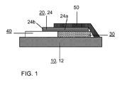
- FIG. 1 shows a first embodiment of a semiconductor device according to the present invention.
- the device comprises a first electrically conductive structure 10.
- the electrically conductive structure comprises a metal foil (or metal-coated foil) such as steel, stainless steel or an aluminum foil having a thickness of 20 to 200 ⁇ m.
- the metal foil 10 forms a first electrode layer 12.
- the semiconductor device further comprises a second electrically conductive structure 20 that comprises at least a second electrode layer 24.
- the second electrode layer 24 is formed by a silver layer having a thickness in the range of 10 -20 nm. If the second electrode layer 24 is less than 10 nm, then relatively large resistive losses will occur in this layer 24. If the thickness of the second electrode layer 24 is substantially greater than 20 nm, e.g. greater than 40 nm, a relatively high loss of light occurs in this layer 24.
- the semiconductor device further comprises an active structure 30 that comprises at least a layer of an organic semiconducting material, such as a light-emitting polymer.
- the active structure is arranged between the first and the second electrically conductive structures 10, 20.
- the active structure 30 may comprise one or more functional layers.
- the active structure comprises at least one layer of a light-emitting material, such as polymeric PPV or layer stacks and mixtures of small molecules possibly including phosphorescent emitters such as Ir(ppy) 3 .
- additional layers may be present, such as a hole injection layer (HIL) such as PEDOT between the layer of light-emitting material and the electrically conductive structure comprising the anode, and or an electron injection layer such as TPBI, TAZ, OXD7, or the like between the layer of light-emitting material and the electrically conductive structure comprising the cathode.
- HIL hole injection layer
- TPBI electron injection layer
- TPBI TPBI, TAZ, OXD7, or the like between the layer of light-emitting material and the electrically conductive structure comprising the cathode.
- the second electrically conductive structure 20 comprises a first portion 24a that forms a cathode and a second portion 24b that forms an external contact to the cathode 24a.
- the first electrically insulating barrier structure 40 comprises at least an electrically insulating barrier layer, e.g. an oxide layer or a nitride layer, or a stack of oxide and nitride layers that, alternate each other.
- a second electrically insulating barrier structure 50 is provided that extends over a part 24a of the second electrically conductive structure 20 formed by the electrode layer 24.
- a portion 24b of the electrode layer that forms the second electrically conductive structure 20 extends laterally beyond the second electrically insulating barrier structure 50.
- the active structure 30 is encapsulated by an encapsulation comprising at least the first electrically conductive structure 10, the first electrically insulating barrier structure 40, the second electrically conductive structure 20 and the second electrically insulating barrier structure 50.
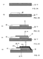
- FIG. 2A to 2E show a method of manufacturing a semiconductor device as shown in Figure 1 .
- the first electrically conductive structure 10 is provided e.g. in the form of a metal foil.
- a polymer or glass substrate may be provided having a metal layer as the first electrically conductive structure material.
- an electrically conductive polymer foil may be used as the first electrically conductive structure.
- the first electrically conductive structure 10 forms a first electrode layer 12. Nevertheless additional electrically conductive layers may be provided in the first electrically conductive structure 10.
- Figure 2B illustrates a second step S2 wherein a first electrically insulating barrier structure 40 is provided that comprises at least an electrically insulating barrier layer on said first electrically conductive structure 10.
- a first electrically insulating barrier structure 40 is provided that comprises at least an electrically insulating barrier layer on said first electrically conductive structure 10.
- Inorganic layers forming the first electrically insulating barrier structure may be applied by all kinds of physical vapour deposition methods such as thermal evaporation, e-beam evaporation, sputtering, magnetron sputtering, reactive sputtering, reactive evaporation, etc. and all kinds of chemical vapour deposition methods such as thermal chemical vapour deposition (CVD), photo assisted chemical vapour deposition (PACVD), plasma enhanced chemical vapour deposition (PECVD), etc.
- physical vapour deposition methods such as thermal evaporation, e-beam evaporation, sputtering, magnetron sputtering, reactive sputtering, reactive evaporation, etc.
- chemical vapour deposition methods such as thermal chemical vapour deposition (CVD), photo assisted chemical vapour deposition (PACVD), plasma enhanced chemical vapour deposition (PECVD), etc.
- a mask layer may be used to apply the first electrically insulating barrier structure 40. For example subsequently a mask layer is applied, at least one layer of an electrically insulating barrier material is deposited and the mask layer is removed. Accordingly a first electrically insulating barrier structure 40 remains at the portions of the first electrically conductive structure 10 that were uncovered by the mask layer.
- the mask layer is for example a patterned photoresist layer that is applied by lithographic techniques. Alternatively the mask layer may be a polymer layer that is patterned by imprinting.
- Another option is to apply first a layer of an electrically insulating barrier material at the first electrically conductive structure and to apply a mask layer at the layer of electrically insulating barrier material.
- the electrically insulating barrier material is etched at those portions left free by the mask layer, therewith obtaining the electrically insulating barrier structure.
- the mask layer may be removed afterwards, e.g. with a solvent.
- the first electrically insulating barrier structure 40 is applied by locally oxidizing the first electrically conductive structure 10.
- the active structure 30 comprising at least a layer of an organic semiconducting material is deposited at the first electrically conductive structure 10.
- the at least one layer may be deposited for example by a printing method, such as inkjet printing, gravure printing, flexographic printing, screen printing, rotary screen printing, etc or by a coating technique such as bar coating, slot-die coating or spin coating.
- a printing method such as inkjet printing, gravure printing, flexographic printing, screen printing, rotary screen printing, etc
- a coating technique such as bar coating, slot-die coating or spin coating.
- thermal evaporation or other vapour phase deposition techniques may be used.
- other methods e.g. methods involving a carrier gas are applicable.
- a second electrically conductive structure 20 that comprises at least a second electrode layer 24 is deposited on the active structure 30.
- the second electrode layer, the cathode in this case, is for example a layer of Ag.
- This layer may be applied by various techniques including thermal evaporation, printing and coating techniques, lamination of a metal layer or the use of ionic liquids.
- a second electrically insulating barrier structure 50 is deposited over the second electrically conductive structure 20.
- the electrically insulating barrier structure 50 is deposited using a suitable mask such that at least a portion 24b of the second electrically conductive structure 20 remains uncovered and forms a feed-through to the second electrode layer 24.
- Figure 3 shows a second embodiment in cross-section.
- Figure 4 show a top view of this embodiment, wherein hidden parts or portions thereof are indicated by dashed lines and visible parts or portions thereof by solid lines.
- the second electrically conductive structure 20 comprises in addition to the second electrode layer 24, an electric supply structure 22.
- the electrical supply structure 22 materials may be used that have an excellent resistance against moisture, such as metals including aluminum and silver, but do not need to be suitable as an electrode material.
- the electrode layer 24 may be manufactured from a material suitable for that purpose. However, as the electrode layer itself need not be exposed to the environment, it does not need to be moisture resistant. Accordingly also sensitive materials like Ba may be used.
- a portion 22b of the electrically conductive structure 22 forming part of the second electrically conductive structure 20 extends laterally beyond the second electrically insulating barrier structure 50.
- a portion 22a of the electrically conductive structure 22 is enclosed by the second electrically insulating barrier structure 50, and electrically contacts the electrode layer 24.
- the active structure 30 is encapsulated by the first electrically conductive structure 10, the first electrically insulating barrier structure 40, the second electrically conductive structure 20 and the second electrically insulating barrier structure 50.
- the electric supply structure 22 of the second electrically conductive structure 20 contributes to the encapsulation, and the electrode layer 24 of the second electrically conductive structure 20 is protected by the encapsulation.
- the first and the second electrically conductive structure 10, 20 are connected to respective poles of an electric power supply 60.
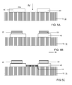
- Figure 5 shows a method of manufacturing the device of Figures 3 and 4 .
- an electric supply structure 22 is applied as is shown in Figure 5B .
- Various options are possible to apply the electric supply structure 22, such as thermal evaporation, sputtering, printing, electroplating, after first applying a plating base, for example with electroless plating, etc.
- FIG. 5C shows the result of a next step, wherein a charge injection layer, e.g. a PEDOT layer 14 is applied over the first electrically conductive structure 10.
- a charge injection layer e.g. a PEDOT layer 14 is applied over the first electrically conductive structure 10.
- This layer can be deposited using a technique that includes patterning of the layer to avoid contact with the electrical supply structure 22. If in practice the charge injection layer 14 did cover the electric supply structure 22 that forms part of the second electrically conductive structure, the effects of shortcuts should be minimized if the charge injection layer 14 is relatively thin, e.g. in the order of 10-20 nm and had a low lateral conductivity.
- the charge injection layer is preferably applied as a suspension by a printing method.
- Figure 5D shows the result of a next step, wherein an active layer 30 is deposited.
- the active-layer is preferably deposited as a suspension by means of a printing method, such as inkjet printing, gravure printing, flexographic printing, screen printing, rotary screen printing, etc or by a coating technique such as bar coating, slot-die coating or spin coating.
- a printing method such as inkjet printing, gravure printing, flexographic printing, screen printing, rotary screen printing, etc
- a coating technique such as bar coating, slot-die coating or spin coating.
- other deposition techniques such as thermal evaporation or another vapour phase deposition technique or a technique involving a carrier gas could be used.
- Figure 5E shows the result of a next step, wherein the second electrode layer 24 is deposited.
- additional electrode layers may be deposited.
- an electrode layer 24 of Ba may be covered with an additional electrode layer of Al.
- the second electrically insulating barrier structure 50 is deposited.
- the electrically insulating barrier structure 50 leaves open a portion 22b of the electric supply structure 22, so that said portion 22b extends laterally beyond the second electrically insulating barrier structure 50.
- the second electrically insulating barrier structure 50 fully covers the second electrode structure 24.
- the first electrically conductive structure 10, the first electrically insulating barrier structure 40, the second electrically conductive structure 20 and the second electrically insulating barrier structure 50 form an encapsulation that encapsulates the active structure 30, and fully covers the second electrode layer 24.
- FIG. 6 shows another variant of an OLED, wherein the charge injection layer 14 is applied upon the first electrically conductive structure 10.
- the first electrically insulating barrier structure 40 is then applied upon the charge-injection layer 14.
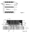
- Figures 7 and 7A show an embodiment of the present invention wherein a patterned electrically insulating layer 45 is applied between the first and the second electrically conductive structure 10, 20.
- Figure 7A is a cross-section according to VIIA-VIIA in Figure 7 .
- part of the surface of the first electrically conductive structure 10 is left free by the electrically insulating barrier layer 40 but covered by the patterned electrically insulating layer 45.
- the patterned electrically insulating layer 45 comprises a pattern of openings 47 through which current is conducted between the electrically conductive structures 10, 20 and through the active structure 30, so that during operation a pattern of light emission becomes visible.
- the patterned electrically insulating layer 45 is a patterned photoresist layer. In this way a very detailed pattern may be obtained.
- the first electrode layer 12 may be a cathode layer and the second electrode layer 24 may be an anode layer.
- the electronic device is an OLED.
- the electronic device may be another device, such as a photovoltaic cell, or an electrochromic device.
Landscapes
- Electroluminescent Light Sources (AREA)
Priority Applications (1)
| Application Number | Priority Date | Filing Date | Title |
|---|---|---|---|
| EP09159689A EP2249412A1 (fr) | 2009-05-07 | 2009-05-07 | Dispositif semi-conducteur organique et procédé de fabrication de celui-ci |
Applications Claiming Priority (1)
| Application Number | Priority Date | Filing Date | Title |
|---|---|---|---|
| EP09159689A EP2249412A1 (fr) | 2009-05-07 | 2009-05-07 | Dispositif semi-conducteur organique et procédé de fabrication de celui-ci |
Publications (1)
| Publication Number | Publication Date |
|---|---|
| EP2249412A1 true EP2249412A1 (fr) | 2010-11-10 |
Family
ID=41077677
Family Applications (1)
| Application Number | Title | Priority Date | Filing Date |
|---|---|---|---|
| EP09159689A Withdrawn EP2249412A1 (fr) | 2009-05-07 | 2009-05-07 | Dispositif semi-conducteur organique et procédé de fabrication de celui-ci |
Country Status (1)
| Country | Link |
|---|---|
| EP (1) | EP2249412A1 (fr) |
Cited By (1)
| Publication number | Priority date | Publication date | Assignee | Title |
|---|---|---|---|---|
| EP2693841A4 (fr) * | 2011-03-29 | 2014-10-22 | Nec Lighting Ltd | Dispositif électroluminescent organique, procédé de fabrication associé, et dispositif d'éclairage électroluminescent organique |
Citations (4)
| Publication number | Priority date | Publication date | Assignee | Title |
|---|---|---|---|---|
| US6835470B1 (en) | 1999-07-28 | 2004-12-28 | Recherche et Developpement du Groupe Cockerill Sambre en abrégé: RD-CS | Electroluminescent device and method for the production thereof |
| US20060087230A1 (en) * | 2004-10-22 | 2006-04-27 | Eastman Kodak Company | Desiccant film in top-emitting OLED |
| US20060246811A1 (en) * | 2005-04-28 | 2006-11-02 | Eastman Kodak Company | Encapsulating emissive portions of an OLED device |
| US20080018244A1 (en) * | 2006-07-24 | 2008-01-24 | Munisamy Anandan | Flexible OLED light source |
-
2009
- 2009-05-07 EP EP09159689A patent/EP2249412A1/fr not_active Withdrawn
Patent Citations (4)
| Publication number | Priority date | Publication date | Assignee | Title |
|---|---|---|---|---|
| US6835470B1 (en) | 1999-07-28 | 2004-12-28 | Recherche et Developpement du Groupe Cockerill Sambre en abrégé: RD-CS | Electroluminescent device and method for the production thereof |
| US20060087230A1 (en) * | 2004-10-22 | 2006-04-27 | Eastman Kodak Company | Desiccant film in top-emitting OLED |
| US20060246811A1 (en) * | 2005-04-28 | 2006-11-02 | Eastman Kodak Company | Encapsulating emissive portions of an OLED device |
| US20080018244A1 (en) * | 2006-07-24 | 2008-01-24 | Munisamy Anandan | Flexible OLED light source |
Cited By (4)
| Publication number | Priority date | Publication date | Assignee | Title |
|---|---|---|---|---|
| EP2693841A4 (fr) * | 2011-03-29 | 2014-10-22 | Nec Lighting Ltd | Dispositif électroluminescent organique, procédé de fabrication associé, et dispositif d'éclairage électroluminescent organique |
| US8963144B2 (en) | 2011-03-29 | 2015-02-24 | Nec Lighting, Ltd. | Organic EL light emitting device, manufacturing method therefor, and organic EL illumination device |
| US9269928B2 (en) | 2011-03-29 | 2016-02-23 | Nec Lighting, Ltd. | Organic EL light emitting device, manufacturing method therefor, and organic EL illumination device |
| US9537114B2 (en) | 2011-03-29 | 2017-01-03 | Nec Lighting, Ltd. | Organic EL light emitting device, manufacturing method therefor, and organic EL illumination device |
Similar Documents
| Publication | Publication Date | Title |
|---|---|---|
| TWI553935B (zh) | 製備光電裝置之方法 | |
| US7011983B2 (en) | Large organic devices and methods of fabricating large organic devices | |
| JP6602832B2 (ja) | 発光装置の作製方法 | |
| US7612367B2 (en) | Photovoltaic component and production method therefor | |
| CN101326655B (zh) | 一种大面积有机二极管器件及其制造方法 | |
| US20120298174A1 (en) | Organic thin film solar cell | |
| CN104521021A (zh) | 具有有机层的封装器件及其制造方法 | |
| US20090101206A1 (en) | Process for manufacturing a photovoltaic or a light emitting polymer device | |
| US20140197424A1 (en) | Optoelectric device and method for manufacturing the same | |
| WO2008132655A2 (fr) | Dispositif photoémetteur à métallisation anodisée | |
| JP5543455B2 (ja) | 統合カプセル封止された電子素子 | |
| CN207068930U (zh) | Oled显示基板和oled显示装置 | |
| CN104737291B (zh) | 用于制造光电子组件的方法和光电子组件 | |
| JP2011529264A5 (fr) | ||
| US11476443B2 (en) | Display panel having thin film encapsulation layer including nanotube layer | |
| US8772776B2 (en) | Electro-optic device and method for manufacturing the same | |
| WO2010093237A1 (fr) | Dispositif optoélectronique et procédé de fabrication dudit dispositif | |
| US20060220528A1 (en) | Light-emitting devices | |
| KR20140116024A (ko) | 인캡슐레이션 방법 및 관련 장치 | |
| US8791487B2 (en) | Zinc oxide-containing transparent conductive electrode | |
| US9257492B2 (en) | Method for producing a passive electronic component, method for producing an optoelectronic assembly and passive electronic component | |
| CN114267808A (zh) | 显示面板及其制备方法 |
Legal Events
| Date | Code | Title | Description |
|---|---|---|---|
| PUAI | Public reference made under article 153(3) epc to a published international application that has entered the european phase |
Free format text: ORIGINAL CODE: 0009012 |
|
| AK | Designated contracting states |
Kind code of ref document: A1 Designated state(s): AT BE BG CH CY CZ DE DK EE ES FI FR GB GR HR HU IE IS IT LI LT LU LV MC MK MT NL NO PL PT RO SE SI SK TR |
|
| AX | Request for extension of the european patent |
Extension state: AL BA RS |
|
| STAA | Information on the status of an ep patent application or granted ep patent |
Free format text: STATUS: THE APPLICATION IS DEEMED TO BE WITHDRAWN |
|
| 18D | Application deemed to be withdrawn |
Effective date: 20110511 |