EP2249471B1 - Direktwechselstromwandler - Google Patents
Direktwechselstromwandler Download PDFInfo
- Publication number
- EP2249471B1 EP2249471B1 EP09715461.1A EP09715461A EP2249471B1 EP 2249471 B1 EP2249471 B1 EP 2249471B1 EP 09715461 A EP09715461 A EP 09715461A EP 2249471 B1 EP2249471 B1 EP 2249471B1
- Authority
- EP
- European Patent Office
- Prior art keywords
- capacitor
- voltage
- power supply
- supply line
- diode
- Prior art date
- Legal status (The legal status is an assumption and is not a legal conclusion. Google has not performed a legal analysis and makes no representation as to the accuracy of the status listed.)
- Active
Links
Images




Classifications
-
- H—ELECTRICITY
- H02—GENERATION; CONVERSION OR DISTRIBUTION OF ELECTRIC POWER
- H02M—APPARATUS FOR CONVERSION BETWEEN AC AND AC, BETWEEN AC AND DC, OR BETWEEN DC AND DC, AND FOR USE WITH MAINS OR SIMILAR POWER SUPPLY SYSTEMS; CONVERSION OF DC OR AC INPUT POWER INTO SURGE OUTPUT POWER; CONTROL OR REGULATION THEREOF
- H02M7/00—Conversion of AC power input into DC power output; Conversion of DC power input into AC power output
- H02M7/02—Conversion of AC power input into DC power output without possibility of reversal
- H02M7/04—Conversion of AC power input into DC power output without possibility of reversal by static converters
- H02M7/12—Conversion of AC power input into DC power output without possibility of reversal by static converters using discharge tubes with control electrode or semiconductor devices with control electrode
- H02M7/125—Avoiding or suppressing excessive transient voltages or currents
-
- H—ELECTRICITY
- H02—GENERATION; CONVERSION OR DISTRIBUTION OF ELECTRIC POWER
- H02P—CONTROL OR REGULATION OF ELECTRIC MOTORS, ELECTRIC GENERATORS OR DYNAMO-ELECTRIC CONVERTERS; CONTROLLING TRANSFORMERS, REACTORS OR CHOKE COILS
- H02P9/00—Arrangements for controlling electric generators for the purpose of obtaining a desired output
- H02P9/10—Control effected upon generator excitation circuit to reduce harmful effects of overloads or transients, e.g. sudden application of load, sudden removal of load, sudden change of load
- H02P9/102—Control effected upon generator excitation circuit to reduce harmful effects of overloads or transients, e.g. sudden application of load, sudden removal of load, sudden change of load for limiting effects of transients
Definitions
- the present invention relates to a direct AC power converting apparatus, and particularly to a technique for preventing an inrush current to a capacitor included in the direct AC power converting apparatus.
- Non-Patent Document 1 which will be described later discloses a direct AC power converting apparatus including a clamp circuit.
- FIG. 12 shows the direct AC power converting apparatus disclosed in the Non-Patent Document 1.
- the reference characters in the figure do not always coincide with those in the Non-Patent Document 1.
- an IPM motor is provided at an output side of the direct AC power converting apparatus.
- an inductance per phase which corresponds to the average value of an effective inductance of the IPM motor is defined as La
- an overload current serving as a criterion for interrupting a current supply to the IPM motor is defined as i
- a voltage between both ends of the clamp capacitor is defined as Vc
- an electrostatic capacitance of the clamp capacitor is defined as Cc
- an line voltage of a three-phase AC power source is defined as Vs
- Vs line voltage of a three-phase AC power source
- Vc 3 2 La Cc i 2 + 2 Vs 2
- FIG. 13 is a graph based on the expression (2), showing a relationship of the voltage between both ends of the clamp capacitor relative to the electrostatic capacitance of the clamp capacitor.
- the voltage Vc between both ends of the clamp capacitor is approximately 1800 V.
- the voltage value exceeds 1200 V which is the device rating of a transistor or a diode for 400V class of power supply voltage.
- the electrostatic capacitance of the clamp capacitor has to be equal to or larger than 200 ⁇ F, based on the expression (2) and FIG. 13 .
- FIG. 14 is a graph showing a relationship of the inrush current (i(( ⁇ - ⁇ )/ ⁇ )) relative to the electrostatic capacitance C.
- the electrostatic capacitance of the clamp capacitor is set at 200 ⁇ F in order to suppress the voltage between both ends of the clamp capacitor charged by a regenerative current to approximately 750 V, the maximum value (inrush current) of the current reaches 150 A, based on the expressions (6) and (7).
- Patent Documents 1 to 4 are disclosed.
- Patent-Document 5 describes a direct type AC power converting device capable of reducing inrush current.
- a control section controls a current-source converter in a state in which a switch is in conduction and performs voltage doubler rectification on a voltage between a neutral phase input line and any of the lines to provide for charging of clamp capacitors. Accordingly, the clap capacitors are charged through a resistor which prevents an inrush current from flowing there-through.
- Patent-Document 6 describes a power conversion apparatus comprising a 2-level converter for converting an AC power being inputted from an AC power supply through a transformer into a DC power, positive side and negative side smoothing capacitors connected to obtain a 3-level DC voltage by dividing the DC output voltage from the two level converter into two, a three level inverter for converting a 3-level DC voltage into an AC voltage, a bidirectionally conductible semiconductor switch provided between the neutral on the secondary side of the transformer and the neutral on the smoothing capacitors, detectors for detecting the quality of electricity of the smoothing capacitors, and a means for controlling the conducting direction of the semiconductor switch to sustain a constant voltage at the neutral of the smoothing capacitors depending on the quality of electricity detected by the detectors.
- Patent Document 7 describes a power supply apparatus using a magnet generator. Provided power supply which increase a DC output when a machine is in a low speed operation, it is suggested to suppress the voltage when the machine is in high speed operation and reduce the DC output when the machine is accelerated to improve acceleration.
- Patent-Document 8 describes a power supply that adequately suppresses a rush current, respective of whether the voltage of an input system is high or low without using a conventional choke coil of a large size, and which improves the efficiency reducing the losses at a steady state in a low input voltage system.
- Non-Patent Document 1 Lixiang Weigh, and Thomas A. Lipo, "Investigation of 9-switch Dual-bridge Matrix Converter Operating under Low Output Power Factor", U.S.A., IEEE ISA2003, vol.1, pp.176-181
- an object of the present invention is to provide a direct AC power converting apparatus capable of reducing an inrush current while preventing an increase in a voltage between both ends of a capacitor by increasing an electrostatic capacitance of the capacitor.
- a first aspect of a direct AC power converting apparatus according to the present invention is directed to a direct AC power converting apparatus including the features of claim 1.
- a second aspect of the direct AC power converting apparatus according to the present invention is directed to the direct AC power converting apparatus of the first aspect, in which the resistor (R1) is provided on the neutral phase input line (ACLn).
- a third aspect of the direct AC power converting apparatus is directed to the direct AC power converting apparatus of the first aspect, in which the resistor (R1) is provided on one of the input lines (ACLr, ACLs, ACLt), and the direct AC power converting apparatus further includes a reactor (Lr, Ls, Lt) connected in parallel with the resistor.
- a fourth aspect of the direct AC power converting apparatus is directed to the direct AC power converting apparatus of any one of the first to third aspects, which further includes a second diode (D3) and a third diode (D4).
- the second diode (D3) has an anode connected to a point between the first diode (D2) and the second capacitor (Cc2), and a cathode connected to the positive-side DC power supply line (L1).
- the third diode (D4) has an anode connected to the negative-side DC power supply line (L2), and a cathode connected to a point between the first diode (D2) and the first capacitor (Cc1).
- an inrush current is prevented from flowing from the multi-phase AC power source to the first capacitor and the second capacitor at a time of an initial operation of the current-source power converter. At this time, the input capacitor is not electrically connected to the first capacitor and the second capacitor.
- the current-source power converter When a pair of the high-arm side switching element and the low-arm side switching element which are connected to one input line is rendered conducting while the switch is conducting, the current-source power converter, together with the neutral phase input line, the first capacitor, and the second capacitor, equivalently forms a voltage doubler rectification circuit. Therefore, a voltage between both ends of a pair of the first capacitor and the second capacitor after being charged has a value twice as high as a voltage value of the multi-phase AC power source.
- the current-source power converter converts a multi-phase AC current flowing among the input lines into a DC current, and supplies the DC current to the first capacitor and the second capacitor. Therefore, the input capacitor is connected in parallel with the first capacitor and the second capacitor. A voltage between both ends of the input capacitor corresponds to a line voltage of the input line, and has a value ⁇ 3 as high as a voltage value of the multi-phase AC power source.
- the voltage between both ends of a pair of the first capacitor and the second capacitor is higher than the voltage between both ends of the input capacitor. Therefore, an inrush current can be effectively prevented from flowing from the input capacitor to the first capacitor and the second capacitor in a case where the input capacitor is connected in parallel with the first capacitor and the second capacitor.
- the resistor is provided on the neutral phase input line. Therefore, by using any input line, the DC current can be supplied to the first capacitor and the second capacitor via the resistor.
- a carrier current component removal filter that removes a carrier current component can be formed with the reactor and the input capacitor. Additionally, since the resistor and the reactor are connected in parallel, voltage pulsations of the input capacitor, which may occur at an initial stage of charging (at a transient time), can be reduced.
- the first capacitor and the second capacitor are charged in a series-connection state and discharged in a parallel-connection state, due to a rectifying function of the first to third diodes.
- the first capacitor and the second capacitor are charged with a regenerative current from the inductive multi-phase load, and discharged when a voltage between both ends of each of the first and second capacitor exceeds a voltage value determined based on a load power factor at the voltage-source power converting apparatus side. That is, since a discharging path can be ensured by using the first capacitor and the second capacitor, an operation equivalent to the operation of the mode disclosed in the Non-Patent Document 1 can be realized even though the path is a passive circuit.
- the motor driving device includes a power source E1, input lines ACLr, ACLs, ACLt, a neutral phase input line ACLn, reactors Lr, Ls, Lt, capacitors Cr, Cs, Ct, a current-source converter 1, DC power supply lines L1, L2, a clamp circuit 2, a voltage-source inverter 3, a motor 4, a control section 5, a resistor R1, and a switch S1.
- the power source E1 is a multi-phase AC power source having a neutral point (not shown), and for example, is a three-phase AC power source. An output of the power source E1 is given to the input lines ACLr, ACLs, ACLt.
- the reactors Lr, Ls, Lt are provided on the input lines ACLr, ACLs, ACLt, respectively.
- the capacitors Cr, Cs, Ct are provided among the respective input lines ACLr, ACLs, ACLt, by being Y-connected with one another, for example. Specifically, the capacitors Cr, Cs are connected in series between the input lines ACLr, ACLs. The capacitors Cs, Ct are connected in series between the input lines ACLs, ACLt. The capacitors Ct, Cr are connected in series between the input lines ACLt, ACLr. They are provided at the input side of the current-source converter 1, and function as a voltage source.
- the capacitors Cr, Cs, Ct can be recognized as input capacitors. On the other hand, it can also be recognized that the capacitors Cr, Cs, Ct cooperate with the reactors Lr, Ls, Lt, respectively, to form a carrier current component removal filter for removing a carrier current component.
- the current-source converter 1 has a plurality of switching elements. By selectively operating the plurality of switching elements, the current-source converter 1 converts three-phase AC voltages applied among the input lines ACLr, ACLs, ACLt into a square-waveform DC voltage having two potentials to supply the DC voltage between the DC power supply lines L1, L2.
- the DC power supply line L1 can be recognized as a positive-side DC power supply line
- the DC power supply line L2 can be recognized as a negative-side DC power supply line to which applied is a potential lower than a potential applied to the DC power supply line L1.
- the current-source converter 1 includes high-arm side transistors Srp, SsP, Stp, low-arm side transistors Srn, Ssn, Stn, and diodes Drp, Drn, Dsp, Dsn, Dtp, Dtn.
- the high-arm side transistor and the low-arm side transistor are simply called “transistors”.
- the cathode of each of the diodes Drp, Dsp, Dtp is connected to the DC power supply line L1
- the anode of each of the diodes Drn, Dsn, Dtn is connected to the DC power supply line L2.
- the emitters of the transistors Srp, Ssp, Stp are connected to the anodes of the diodes Drp, Dsp, Dtp, respectively, and the collectors of the transistors Srn, Ssn, Stn are connected to the cathodes of the diodes Drn, Dsn, Dtn.
- the collector of the transistor Srp and the emitter of the transistor Srn are commonly connected to the input line ACLr.
- the collector of the transistor Ssp and the emitter of the transistor Ssn are commonly connected to the input line ACLs.
- the collector of the transistor Stp and the emitter of the transistor Stn are commonly connected to the input line ACLt.
- a pair of a transistor and a diode that is connected in series with the transistor (for example, a pair of the transistors Srp and the diode Drp) can be recognized as a switching element having a reverse blocking capability.
- the control section 5 gives a switching signal to the base of each of the transistors Srp, Srn, Ssp, Ssn, Stp, Stn, so that the current-source converter 1 converts the three-phase AC voltages into the square-waveform DC voltage having two potentials.
- the clamp circuit 2 includes clamp capacitors Cc1, Cc2, and a diode D1.
- the diode D1 is provided between the DC power supply lines L1, L2, and has the anode thereof connected to the DC power supply line L1 side and the cathode thereof connected to the DC power supply line L2 side.
- Each of the clamp capacitors Cc1, Cc2 is connected in series with the diode D1.
- the clamp capacitors Cc1, Cc2, and the diode D1 are connected in series with one another.
- the clamp circuit 2 of this type can suppress an increase in the voltage between the DC power supply lines L1, L2, which may be caused by a return current flowing from the voltage-source inverter 3 to the current-source converter 1. Additionally, since the clamp capacitors Cc1, Cc2 divide the voltage between the DC power supply lines L1, L2, the voltage between both ends of each clamp capacitor Cc1, Cc2 can be reduced.
- the neutral phase input line ACLn connects the neutral point of the power source E1 to a point between the clamp capacitors Cc1, Cc2.
- the resistor R1 is inserted in the neutral phase input line ACLn.
- the switch S1 is provided on the neutral phase input line ACLn and in series with the resistor R1.
- the voltage-source inverter 3 converts the square-waveform DC voltage between the DC power supply lines L1, L2, into a square-waveform AC voltage, and outputs the AC voltage to the motor 4. More specifically, the voltage-source inverter 3 includes high-arm side transistors Sup, Svp, Swp, low-arm side transistors Sun, Svn, Swn, and diodes Dup, Dun, Dvp, Dvn, Dwp, Dwn.
- the collectors of the transistors Sup. Svp, Swp, and the cathodes of the diodes Dup, Dvp, Dwp are connected to the DC power supply line L1.
- the emitters of the transistors Sun, Svn, Swn, and the anodes of the diodes Dun, Dvn, Dwn are connected to the DC power supply line L2.
- the emitter of the transistor Sup, the collector of the transistor Sun, the anode of the diode Dup, and the cathode of the diode Dun are commonly connected to the motor 4.
- the emitter of the transistor Svp, the collector of the transistor Svn, the anode of the diode Dvp, and the cathode of the diode Dvn are commonly connected to the motor 4.
- the emitter of the transistor Swp, the collector of the transistor Swn, the anode of the diode Dwp, and the cathode of the diode Dwn are commonly connected to the motor 4.
- control section 5 gives a switching signal to the base of each of the transistors Sup, Sun, Svp, Svn, Swp, Swn, so that the voltage-source inverter 3 converts the square-waveform DC voltage between the DC power supply lines L1, L2, into a square-waveform AC voltage, and outputs the AC voltage to the motor 4.
- the motor 4 is for example a three-phase AC motor.
- An inductance component and a resistorance component of the motor 4 are represented by coils Lu, Lv, Lw and resistors Ru, Rv, Rw, respectively.
- the resistors Ru, Rv, Rw are connected in series with the coils Lu, Lv, Lw, respectively. These series connections correspond to the respective phases of the motor 4.
- One ends of the series connections are connected to a point between the transistors Sup, Sun, to a point between the transistors Svp, Svn, and to a point between the transistors Swp, Swn, respectively.
- the other ends of the series connections are commonly connected at a neutral point N.
- the square-waveform AC voltage is given from the voltage-source inverter 3, and the AC current that drives the motor 4 is smoothed due to the inductance component of the motor 4.
- the motor 4 converts the square-waveform AC voltage, which is given from the voltage-source inverter 3, into an AC current.
- the AC current flowing in the motor 4 charges the capacitors Cr, Cs, Ct via the voltage-source inverter 3 and the current-source converter 1, and is converted into an AC voltage.
- the motor 4 can be recognized as a current source with respect to the current-source converter 1.
- the control section 5 controls a selection operation of the switch S1 and the transistors of the current-source converter 1. While rendering the switch S1 conducting, the control section 5 renders conducting a pair of the high-arm side transistor and the low-arm side transistor connected to any one of the input lines ACLr, ACLs, ACLt. As a result, a one-phase line current flowing through one of the input lines (for example, the input line ACLr) and the neutral phase input line ACLn is subjected to voltage doubler rectification, and supplied to the clamp capacitors Cc1, Cc2 via the resistor R1. Then, after a predetermined time period elapses, the control section 5 renders the switch S1 non-conducting.
- control section 5 includes a power supply detection section 51 and a switching control section 52.
- the power supply detection section 51 detects an AC current flowing through predetermined two phases (for example, the input lines ACLr, ACLs) of the power source E1.
- the switching control section 52 gives switching signals to the transistors of the current-source converter 1.
- FIG. 2 is a flowchart showing an operation of the control section 5.
- step ST1 the power supply detection section 51 receives an activation command from an external CPU for example. Then, in step ST2, the power supply detection section 51 having received the activation command detects, for example, an AC current flowing through predetermined two phases (for example, the input lines ACLr, ACLs) of the power source E1. When the power supply detection section 51 detects a proper AC current, step ST3 is performed. When the AC current is not properly detected (when no AC current is given to the current-source converter 1), an error is informed and the operation is stopped, for example.
- step ST1, ST2 and later-described steps ST3 to ST7 When an operation (steps ST1, ST2 and later-described steps ST3 to ST7) for charging the clamp capacitors Cc1, Cc2 is performed with no AC current being supplied, the clamp capacitors Cc1, Cc2 are charged with no voltage. Then, when the operation mode is changed to a normal operation with the clamp capacitors Cc1, Cc2 being charged with no voltage, and an AC current is given to the current-source converter 1 in the normal operation, the current flows into the clamp capacitors Cc1, Cc2 not via the current-limiting resistor R1 because the switch S1 is not conducting in the normal operation. As a result, an inrush current flows. In the present embodiment, flowing of such an inrush current can be prevented by the operation of step ST2 mentioned above.
- step ST3 the power supply detection section 51 transmits a switching signal to the switch S1 to render the switch S1 conducting.
- step ST4 the switching control section 52 performs voltage doubler rectification on a one-phase voltage between one of the input lines (for example, the input line ACLr) and the neutral phase input line ACLn, to serve for charging of the clamp capacitors Cc1, Cc2. Specifically, the switching control section 52 starts controlling the transistors Srp, Srn, for example.
- FIG. 3 is a diagram showing a voltage Vrn between the input line ACLr and the neutral phase input line ACLn, and conduction/non-conduction states of the transistors Srp, Srn. In FIG. 3 , when a potential at the input line ACLr side is high, the voltage Vrn is positive.
- the switching control section 52 renders a pair of the transistors Srp, Srn conducting, irrespective of whether the polarity of the phase voltage Vrn is positive or negative.
- a circuit made up of the power source E1, the input line ACLr, the transistors Srp, Srn, the clamp capacitors Cc1, Cc2, and the neutral phase input line ACLn equivalently forms a voltage doubler rectification circuit. Since the resistor R1 is inserted in any of charging paths for charging the clamp capacitors Cc1, Cc2, a DC voltage is applied to the clamp capacitors Cc1, Cc2 via the resistor R1. This can prevent an inrush current from flowing from the power source E1 to the clamp capacitors Cc1, Cc2.
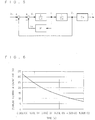
- FIG. 4 is a diagram showing the circuit.
- D 1/L
- E R/L
- F 1/LC
- FIG. 6 graphically illustrates the expression (9), and shows a relationship of a current flowing in the capacitor relative to time.
- FIG. 6 shows a result obtained when an inductance of the reactor L is 1 mH, an electrostatic capacitance of the capacitor C is 330 ⁇ F, a resistance value of the resistor R is 10 ⁇ , and the power supply voltage Vs is 400V.
- step ST5 the power supply detection section 51 determines whether or not a predefined time period has elapsed after step ST4 started.
- step ST5 is performed again.
- the power supply detection section 51 renders the switch S1 non-conducting in step ST6.
- step ST4 for example, a pair of the transistors Srp, Srn are rendered conducting, and the transistors Ssp, Ssn, Stp, Stn are non-conducting. Therefore, the capacitors Cr, Cs, Ct and the clamp capacitors Cc1, Cc2 are not connected to each other. Accordingly, even when the capacitors Cr, Cs, Ct are charged, flowing of an inrush current from the capacitors Cr, Cs, Ct to the clamp capacitors Cc1, Cc2 can be prevented.
- step ST7 the direct AC power converting apparatus is activated, and the operation is changed to the normal operation. More specifically, in order to switch a switching operation of the current-source converter 1 into a normal operation mode, the current-source converter 1 is reactivated, and additionally the voltage-source inverter 3 is activated.
- the switching control section 52 gives switching signals to the transistors Srp, Srn, Ssp, Ssn, Stp, Stn to operate the current-source converter 1, so that an AC voltage inputted from the input lines ACLr, ACLs, ACLt is converted into a square-waveform DC voltage having two potentials, and the DC voltage is supplied to the DC power supply lines L1, L2.
- the voltage-source inverter 3 operates in synchronization with the current-source converter 1, converts the square-waveform DC voltage between the DC power supply lines L1, L2 into a square-waveform AC voltage, and applies the AC voltage to the motor 4.
- step ST4 the DC voltage which has been subjected to the voltage doubler rectification is applied to the clamp capacitors Cc1, Cc2. Therefore, a voltage between both ends of a pair of the clamp capacitors Cc1, Cc2 is higher (specifically 2/ ⁇ 3 times higher) than a voltage between both ends of a pair of the capacitors Cr, Cs, for example. Therefore, in starting the normal operation, a current initially flowing from the capacitors Cr, Cs to the clamp capacitors Cc1, Cc2 can be effectively prevented from flowing as an inrush current.
- the present motor driving device can prevent an inrush current from flowing from the power source E1 to the clamp capacitors Cc1, Cc2. Moreover, in starting the normal operation, an inrush current can be effectively prevented from flowing from the capacitors Cr, Cs, Ct to the clamp capacitors Cc1, Cc2. Furthermore, it suffices that a pair of the transistors Srp, Srn are rendered conducting, and it is not necessary to perform a switching control based on a phase of the power supply voltage, for example. Therefore, the switching signal can be easily generated.
- a reactor is generally provided at an output of a current-source converter, and therefore a current-limiting resistor is not provided in the current-source converter.
- a current-limiting resistor is not provided in the current-source converter.
- FIG. 7 a conceptual configuration of a motor driving device is shown in FIG. 7 .
- the motor driving device shown in FIG. 7 is the same as the motor driving device shown in FIG. 1 , except for the clamp circuit 2.
- illustration of the circuits in stages subsequent to the clamp circuit 2 is omitted.
- the clamp circuit 2 includes the clamp capacitors Cc1, Cc2 and diodes D2 to D4.
- the clamp capacitor Cc1 is connected between the DC power supply lines L1, L2.
- the clamp capacitor Cc2 is connected in series with the clamp capacitor Cc1, and provided at the DC power supply line L2 side relative to the clamp capacitor Cc1.
- the diode D2 is provided between the clamp capacitors Cc1, Cc2, and has the anode thereof connected to the clamp capacitor Cc1 and the cathode thereof connected to the clamp capacitor Cc2.
- the diode D3 has the anode thereof connected to a point between the clamp capacitor Cc2 and the diode D2, and the cathode thereof connected to the DC power supply line L1.
- the diode D4 has the anode thereof connected to the DC power supply line L2, and the cathode thereof connected to a point between the clamp capacitor Cc1 and the diode D2.
- the clamp circuit 2 of this type when a current flowing in the motor 4 delays behind a voltage between the DC power supply lines L1, L2 due to a load power factor at the voltage-source inverter 3 side, a return current flows from the motor 4 to the DC power supply lines L1, L2 in a predetermined time period, and the clamp capacitors Cc1, Cc2 are charged in a state of being connected in series with each other.
- a charging voltage (a voltage between both ends of a pair of the clamp capacitors Cc1, Cc2) at this time is also determined based on the load power factor.
- the voltages of the clamp capacitors Cc1, Cc2 act to obtain equilibrium, in a case where a discharging current is larger than a charging current.
- the return current from the motor 4 can be charged, and discharged again to be supplied to the motor 4 again. Therefore, the motor 4 can be efficiently driven. Moreover, since the clamp circuit 2 does not require a so-called active device such as a switching element, power consumption and manufacturing costs can be reduced.
- FIG. 8 a conceptual configuration of a motor driving device is shown in FIG. 8 .
- the conceptual configuration of the present motor driving device is the same as that of the motor driving device shown in FIG. 7 , except for resistors R1 to R3 and an auxiliary switch Sr.
- FIG. 8 illustration of the circuits in stages subsequent to the clamp circuit 2 is omitted.
- a mode of the clamp circuit 2 may be the one shown in FIG. 1 .
- the resistors R1 to R3 are inserted in the input lines ACLr, ACLs, ACLt, respectively.
- the auxiliary switch Sr is connected in series with any of the reactors Lr to Lt. In an exemplary mode illustrated in FIG. 8 , the auxiliary switch Sr is connected in series with the reactor Lr.
- the reactors Ls, Lt are connected in parallel with the resistors R2, R3, respectively.
- a pair of the auxiliary switch Sr and the reactor Lr are connected in parallel with the resistor R1.
- the power supply detection section 51 can control a selection operation of the auxiliary switch Sr.
- step ST6 an operation of the control section 5 is the same as the operation shown in the flowchart of FIG. 2 , except for step ST6.
- the power supply detection section 51 renders the switch S1 non-conducting, and renders the auxiliary switch Sr conducting.
- step ST4 the switching control section 52 preferably outputs switching signals to the current-source converter 1 as shown in FIG. 3 .
- the switch S1 is rendered conducting in step ST3, and at the time when the current-source converter 1 is controlled in step ST4, the auxiliary switch Sr is non-conducting. Therefore, the AC current flowing in the input line ACLr and the neutral phase input line ACLn inevitably flows through the resistor R1. Thus, flowing of an inrush current to the clamp capacitors Cc1, Cc2 can be effectively prevented. It may also be acceptable that the auxiliary switch Sr is not provided and a part of the AC current flowing in the input line ACLr and the neutral phase input line ACLn flows to the clamp capacitors Cc1, Cc2 via the reactor Lr. In this case as well, since another part of the AC current goes through the resistor R1, the inrush current can be reduced. Moreover, as for the AC current going through the reactor Lr, the inrush current can be also reduced by a resistor component of the reactor Lr, for example.
- the resistors R1 to R3 can improve input/output transient characteristics of the capacitors Cr, Cs, Ct.
- a specific description will be given.
- FIG. 9 is a diagram showing a configuration of the circuit.
- a voltage Vo between both ends of the capacitor C is recognized as an output.
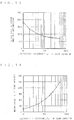
- FIG. 10 is a Bode diagram showing frequency characteristics of the transfer function.
- FIG. 10 shows results which are obtained in three cases where a resistance value of the resistor R is 10 ⁇ , 30 ⁇ , and 100 ⁇ , where an inductance of the reactor L is 1.5 mH and an electrostatic capacitance of the capacitor C is 10 ⁇ F.
- FIG. 11 shows a voltage Vrt, a voltage between both ends of a pair of the capacitors Cr, Ct, a voltage between both ends of a pair of the clamp capacitors Cc1, Cc2, and a voltage between the DC power supply lines L1, L2, in the motor driving device of FIG. 8 using the carrier current component removal filter as described above. Note that FIG. 11 shows results obtained when the resistance value of the resistor R1 is 10 ⁇ and 100 ⁇ .
- damping is produced by the resistance value of the resistor R1, whereby it is possible to reduce a voltage (transient voltage) applied to each of the capacitors Cr, Ct and the clamp capacitors Cc1, Cc2 in a transient period (see the results obtained when the resistance value is 10 ⁇ and 100 ⁇ ).
Landscapes
- Engineering & Computer Science (AREA)
- Power Engineering (AREA)
- Inverter Devices (AREA)
- Rectifiers (AREA)
- Control Of Ac Motors In General (AREA)
Claims (4)
- Direktwechselstromwandlervorrichtung, umfassend:eine Vielzahl von Eingangsleitungen (ACLr, ACLs, ACLt), die mit einer mehrphasigen Wechselstrom-Energiequelle (E1) verbunden sind;eine positivseitige Gleichstromversorgungsleitung (L1);eine negativseitige Gleichstromversorgungsleitung (L2), an die ein Potential angelegt ist, das niedriger als ein Potential ist, das an die positivseitige Gleichstromversorgungsleitung (L1) angelegt ist;einen Stromquellenwandler (1), der beinhaltet:hocharmseitige Schaltelemente (Drp+Srp, Dsp+Ssp, Dtp+Stp) und niederarmseitige Schaltelemente (Drn+Srn, Dsn+Ssn, Dtn+Stn),wobei jedes der hocharmseitigen Schaltelemente (Drp+Srp, Dsp+Ssp, Dtp+Stp) eine Rückwärtssperrfähigkeit hat und zwischen der positivseitigen Gleichstromversorgungsleitung (L1) und einer entsprechenden der Eingangsleitungen (ACLr, ACLs, ACLt) verbunden ist,wobei jedes der niederarmseitigen Schaltelemente (Drn+Srn, Dsn+Ssn, Dtn+Stn) eine Rückwärtssperrfähigkeit hat und zwischen der negativseitigen Gleichstromversorgungsleitung (L2) und einer entsprechenden der Eingangsleitungen (ACLr, ACLs, ACLt) verbunden ist,wobei der Stromquellenwandler konfiguriert ist zumUmwandeln einer mehrphasigen Wechselspannung, die zwischen den Eingangsleitungen (L1, L2) angelegt ist, in eine Rechteckwellenform-Gleichspannung mit zwei Potentialen, durch einen Auswahlbetrieb der hocharmseitigen Schaltelemente (Drp+Srp, Dsp+Ssp, Dtp+Stp) und der niederarmseitigen Schaltelemente (Drn+Srn, Dsn+Ssn, Dtn+Stn); undAnlegen der Gleichspannung zwischen der positivseitigen Gleichstromversorgungsleitung (L1) und der negativseitigen Gleichstromversorgungsleitung (L2);eine Vielzahl von Eingangskondensatoren (Cr, Cs, Ct), jeweils zwischen den einen von den Eingangsleitungen (L1, L2) bereitgestellt und konfiguriert, als jeweils eine Spannungsquelle zu fungieren;eine erste Diode (D1; D2), einen ersten Kondensator (CC1) und einen zweiten Kondensator (Cc2), wobei die erste Diode (D1; D2), der erste Kondensator (CC1) und der zweite Kondensator (Cc2) in Serie zwischen der positivseitigen Gleichstromversorgungsleitung (L1) und der negativseitigen Gleichstromversorgungsleitung (L2) verbunden sind, sodass eine Anode der ersten Diode (D1) mit der positivseitigen Gleichstromversorgungsleitungsseite (L1) verbunden ist und eine Kathode der ersten Diode mit dem ersten Kondensator (Cc1) verbunden ist oder wobeider erste Kondensator (Cc1), die erste Diode (D2) und der zweite Kondensator (Cc2) in Serie zwischen der positivseitigen Gleichstromversorgungsleitung (L1) und der negativseitigen Gleichstromversorgungsleitung (L2) verbunden sind, sodass eine Anode der ersten Diode (D1) mit dem ersten Kondensator (Cc1) verbunden ist und eine Kathode der ersten Diode mit dem zweiten Kondensator (Cc2) verbunden ist;eine neutrale Phaseneingangsleitung (ACLn), die konfiguriert ist, einen neutralen Punkt der mehrphasigen Wechselstrom-Energiequelle und einen Punkt zwischen dem ersten Kondensator (Cc1) und dem zweiten Kondensator (Cc2) zu verbinden;einen Schalter (S1), der in der neutralen Phaseneingangsleitung eingefügt ist;einen Spannungsquellen-Energiewandler (3), der konfiguriert ist, die Gleichspannung in eine Rechteckwellenform-Wechselspannung umzuwandeln und konfiguriert ist, die Wechselspannung an einen induktiven mehrphasigen Stromabnehmer (4) auszugeben;einen Widerstand (R1), der in eine der mehreren Eingangsleitungen (ACLr, ACLs, ACLt) und die neutrale Phaseneingangsleitung (ACLn) eingefügt ist; undeinen Steuerabschnitt (5), der konfiguriert ist, ein Paar (Srp, Srn) des hocharmseitigen Schaltelements (Drp+Srp, Dsp+Ssp, Dtp+Stp) und des niederarmseitigen Schaltelements (Drn+Srn, Dsn+Ssn, Dtn+Stn) leitend zu machen, ungeachtet dessen, ob die Polarität der Phasenspannung (Vrn) positiv oder negativ ist, während der Schalter (S1) leitet, wobei das Paar (Srp, Srn) des hocharmseitigen Schaltelements (Drp+Srp, Dsp+Ssp, Dtp+Stp) und des niederarmseitigen Schaltelements (Drn+Srn, Dsn+Ssn, Dtn+Stn) mit derselben einen der Eingangsleitungen (ACLr, ACLs, ACLt) verbunden ist und zum Laden des ersten Kondensators (Cc1) und des zweiten Kondensators (Cc2) über den Widerstand (R1) dient und konfiguriert ist, den Schalter (S1) nichtleitend zu machen, nachdem eine vorbestimmte Zeitdauer verstreicht.
- Direktwechselstromwandlervorrichtung nach Anspruch 1, wobei der Widerstand (R1) auf der neutralen Phaseneingangsleitung (ACLn) bereitgestellt ist.
- Direktwechselstromwandlervorrichtung nach Anspruch 1, wobei
der Widerstand (R1) auf einer der Eingangsleitungen (ACLr, ACLs, ACLt) bereitgestellt ist, und
die Direktwechselstromwandlervorrichtung weiter eine Drosselspule (Lr, Ls, Lt) umfasst, die parallel mit dem Widerstand (R1) verbunden ist. - Direktwechselstromwandlervorrichtung nach einem der Ansprüche 1 bis 3, weiter umfassend:eine zweite Diode (D3) mit einer Anode, die mit einem Punkt zwischen der ersten Diode (D2) und dem zweiten Kondensator (Cc2) verbunden ist, und eine Kathode, die mit der positivseitigen Gleichstromversorgungsleitung (L1) verbunden ist; undeine dritte Diode (D4) mit einer Anode, die mit der negativseitigen Gleichstromversorgungsleitung (L2) verbunden ist, und eine Kathode, die mit einem Punkt zwischen der ersten Diode (D2) und dem ersten Kondensator (Cc1) verbunden ist.
Applications Claiming Priority (2)
| Application Number | Priority Date | Filing Date | Title |
|---|---|---|---|
| JP2008047897A JP5146011B2 (ja) | 2008-02-28 | 2008-02-28 | 直接形交流電力変換装置 |
| PCT/JP2009/051751 WO2009107461A1 (ja) | 2008-02-28 | 2009-02-03 | 直接形交流電力変換装置 |
Publications (3)
| Publication Number | Publication Date |
|---|---|
| EP2249471A1 EP2249471A1 (de) | 2010-11-10 |
| EP2249471A4 EP2249471A4 (de) | 2017-09-13 |
| EP2249471B1 true EP2249471B1 (de) | 2019-05-15 |
Family
ID=41015864
Family Applications (1)
| Application Number | Title | Priority Date | Filing Date |
|---|---|---|---|
| EP09715461.1A Active EP2249471B1 (de) | 2008-02-28 | 2009-02-03 | Direktwechselstromwandler |
Country Status (7)
| Country | Link |
|---|---|
| US (1) | US8374005B2 (de) |
| EP (1) | EP2249471B1 (de) |
| JP (1) | JP5146011B2 (de) |
| KR (1) | KR101327692B1 (de) |
| CN (1) | CN101960702B (de) |
| AU (1) | AU2009219515C1 (de) |
| WO (1) | WO2009107461A1 (de) |
Families Citing this family (15)
| Publication number | Priority date | Publication date | Assignee | Title |
|---|---|---|---|---|
| JP4238935B1 (ja) * | 2007-08-28 | 2009-03-18 | ダイキン工業株式会社 | 直接形交流電力変換装置 |
| WO2010131344A1 (ja) * | 2009-05-13 | 2010-11-18 | 三菱電機株式会社 | 電力変換装置および電力変換装置のコンデンサ電圧の制御方法 |
| US10772499B2 (en) * | 2009-07-25 | 2020-09-15 | Lensar, Inc. | System and method for measuring tilt |
| JP4951053B2 (ja) * | 2009-11-20 | 2012-06-13 | ダイヤモンド電機株式会社 | インダイレクトマトリクスコンバータ |
| JP5062347B1 (ja) * | 2011-05-02 | 2012-10-31 | ダイキン工業株式会社 | 電力変換回路及び空気調和装置 |
| JP5115636B2 (ja) * | 2011-05-02 | 2013-01-09 | ダイキン工業株式会社 | 電力変換回路および空気調和装置 |
| KR101621994B1 (ko) * | 2011-12-30 | 2016-05-17 | 엘에스산전 주식회사 | 회생형 고압 인버터의 제어장치 |
| US9099934B2 (en) * | 2012-01-10 | 2015-08-04 | Yaskawa America, Inc. | Three phase active rectifier system |
| JP5429316B2 (ja) * | 2012-03-02 | 2014-02-26 | ダイキン工業株式会社 | インダイレクトマトリックスコンバータ |
| CN103078493B (zh) * | 2013-01-18 | 2015-02-25 | 广州金升阳科技有限公司 | 一种升压电路 |
| CN103178738A (zh) * | 2013-02-27 | 2013-06-26 | 薛建仁 | 新型高效节能pwm工业整流电源 |
| EP3217522A1 (de) * | 2016-03-08 | 2017-09-13 | Siemens Aktiengesellschaft | Rückspeisefähige gleichrichtervorrichtung |
| US9919610B1 (en) * | 2017-01-12 | 2018-03-20 | The Florida International University Board Of Trustees | Wireless power electronics and controls |
| CN114270688A (zh) * | 2019-08-30 | 2022-04-01 | 三菱电机株式会社 | 电力变换装置以及空气调节机 |
| DE102019131410A1 (de) * | 2019-11-21 | 2021-05-27 | Ebm-Papst Mulfingen Gmbh & Co. Kg | Vorrichtung zur effizienten netzartunabhängigen Zwischenkreisaufbereitung |
Family Cites Families (20)
| Publication number | Priority date | Publication date | Assignee | Title |
|---|---|---|---|---|
| JPH0265667A (ja) | 1988-08-27 | 1990-03-06 | Hitachi Ltd | コンバータの制御装置 |
| JPH02265667A (ja) | 1989-04-05 | 1990-10-30 | Nippon Paint Co Ltd | ロールコータによる帯板の塗装装置 |
| JPH05292759A (ja) | 1992-04-13 | 1993-11-05 | Shinko Electric Co Ltd | エンジン式発電装置 |
| JPH07289766A (ja) * | 1994-04-28 | 1995-11-07 | Matsushita Electric Ind Co Ltd | 工業用ミシン駆動装置 |
| JPH0879963A (ja) | 1994-09-06 | 1996-03-22 | Daikin Ind Ltd | 電力変換制御装置における故障診断装置 |
| DE69533001T2 (de) * | 1995-10-06 | 2005-05-04 | Hitachi, Ltd. | Motorregler |
| US5841647A (en) * | 1996-10-07 | 1998-11-24 | Kabushiki Kaisha Toshiba | Power conversion system |
| JPH11285253A (ja) * | 1998-03-26 | 1999-10-15 | Omron Corp | 電源装置 |
| JPH11332239A (ja) | 1998-05-15 | 1999-11-30 | Fuji Electric Co Ltd | 単相三線電源用電力変換装置 |
| US6118676A (en) * | 1998-11-06 | 2000-09-12 | Soft Switching Technologies Corp. | Dynamic voltage sag correction |
| JP2000341967A (ja) * | 1999-05-26 | 2000-12-08 | Matsushita Electric Works Ltd | インバータ装置 |
| US6018473A (en) * | 1999-05-26 | 2000-01-25 | Xerox Corporation | Power supply and printing machine containing same |
| KR20010001187A (ko) * | 1999-06-02 | 2001-01-05 | 구자홍 | 자동 전압 전환장치 |
| JP3681050B2 (ja) * | 1999-11-15 | 2005-08-10 | 国産電機株式会社 | 磁石発電機を用いた電源装置 |
| US6995992B2 (en) | 2003-06-20 | 2006-02-07 | Wisconsin Alumni Research Foundation | Dual bridge matrix converter |
| JP4279640B2 (ja) | 2003-09-26 | 2009-06-17 | 東芝三菱電機産業システム株式会社 | 電力変換装置 |
| JP4021431B2 (ja) | 2004-08-10 | 2007-12-12 | ファナック株式会社 | コンバータ装置、インバータ装置及びdcリンク電圧の制御方法 |
| US7492616B2 (en) | 2005-03-25 | 2009-02-17 | Lineage Power Corporation | Modulation controller, method of controlling and three phase converter system employing the same |
| KR100700787B1 (ko) * | 2005-08-16 | 2007-03-27 | 엘지전자 주식회사 | 영상표시기기의 전원 제어장치 |
| JP4238935B1 (ja) * | 2007-08-28 | 2009-03-18 | ダイキン工業株式会社 | 直接形交流電力変換装置 |
-
2008
- 2008-02-28 JP JP2008047897A patent/JP5146011B2/ja active Active
-
2009
- 2009-02-03 AU AU2009219515A patent/AU2009219515C1/en active Active
- 2009-02-03 WO PCT/JP2009/051751 patent/WO2009107461A1/ja not_active Ceased
- 2009-02-03 KR KR1020107016914A patent/KR101327692B1/ko not_active Expired - Fee Related
- 2009-02-03 CN CN200980106667.7A patent/CN101960702B/zh active Active
- 2009-02-03 EP EP09715461.1A patent/EP2249471B1/de active Active
- 2009-02-03 US US12/812,892 patent/US8374005B2/en active Active
Non-Patent Citations (1)
| Title |
|---|
| None * |
Also Published As
| Publication number | Publication date |
|---|---|
| EP2249471A1 (de) | 2010-11-10 |
| WO2009107461A1 (ja) | 2009-09-03 |
| US20100296321A1 (en) | 2010-11-25 |
| KR101327692B1 (ko) | 2013-11-11 |
| US8374005B2 (en) | 2013-02-12 |
| JP2009207300A (ja) | 2009-09-10 |
| EP2249471A4 (de) | 2017-09-13 |
| AU2009219515C1 (en) | 2012-11-08 |
| JP5146011B2 (ja) | 2013-02-20 |
| KR20100097756A (ko) | 2010-09-03 |
| AU2009219515B2 (en) | 2012-05-24 |
| CN101960702A (zh) | 2011-01-26 |
| CN101960702B (zh) | 2013-09-11 |
| AU2009219515A1 (en) | 2009-09-03 |
Similar Documents
| Publication | Publication Date | Title |
|---|---|---|
| EP2249471B1 (de) | Direktwechselstromwandler | |
| EP2184843B1 (de) | Direktwechselstromrichter | |
| US8310848B2 (en) | Direct AC power converting apparatus | |
| EP2178199B1 (de) | Direktstromwandler | |
| US9496790B2 (en) | Power conversion device | |
| JP2009017772A (ja) | Dc/dc電力変換装置 | |
| JP2010119239A (ja) | Smes装置、smes用インターフェース装置及びその駆動方法 | |
| JP2010148204A (ja) | 電力変換装置 |
Legal Events
| Date | Code | Title | Description |
|---|---|---|---|
| PUAI | Public reference made under article 153(3) epc to a published international application that has entered the european phase |
Free format text: ORIGINAL CODE: 0009012 |
|
| 17P | Request for examination filed |
Effective date: 20100810 |
|
| AK | Designated contracting states |
Kind code of ref document: A1 Designated state(s): AT BE BG CH CY CZ DE DK EE ES FI FR GB GR HR HU IE IS IT LI LT LU LV MC MK MT NL NO PL PT RO SE SI SK TR |
|
| AX | Request for extension of the european patent |
Extension state: AL BA RS |
|
| DAX | Request for extension of the european patent (deleted) | ||
| RA4 | Supplementary search report drawn up and despatched (corrected) |
Effective date: 20170817 |
|
| RIC1 | Information provided on ipc code assigned before grant |
Ipc: H02M 7/48 20070101AFI20170810BHEP Ipc: H02M 7/12 20060101ALI20170810BHEP Ipc: H02P 9/10 20060101ALI20170810BHEP Ipc: H02P 27/06 20060101ALI20170810BHEP |
|
| GRAP | Despatch of communication of intention to grant a patent |
Free format text: ORIGINAL CODE: EPIDOSNIGR1 |
|
| STAA | Information on the status of an ep patent application or granted ep patent |
Free format text: STATUS: GRANT OF PATENT IS INTENDED |
|
| INTG | Intention to grant announced |
Effective date: 20181102 |
|
| RIN1 | Information on inventor provided before grant (corrected) |
Inventor name: SAKAKIBARA, KENICHI |
|
| GRAJ | Information related to disapproval of communication of intention to grant by the applicant or resumption of examination proceedings by the epo deleted |
Free format text: ORIGINAL CODE: EPIDOSDIGR1 |
|
| STAA | Information on the status of an ep patent application or granted ep patent |
Free format text: STATUS: REQUEST FOR EXAMINATION WAS MADE |
|
| GRAP | Despatch of communication of intention to grant a patent |
Free format text: ORIGINAL CODE: EPIDOSNIGR1 |
|
| STAA | Information on the status of an ep patent application or granted ep patent |
Free format text: STATUS: GRANT OF PATENT IS INTENDED |
|
| INTC | Intention to grant announced (deleted) | ||
| INTG | Intention to grant announced |
Effective date: 20190109 |
|
| GRAS | Grant fee paid |
Free format text: ORIGINAL CODE: EPIDOSNIGR3 |
|
| GRAA | (expected) grant |
Free format text: ORIGINAL CODE: 0009210 |
|
| STAA | Information on the status of an ep patent application or granted ep patent |
Free format text: STATUS: THE PATENT HAS BEEN GRANTED |
|
| AK | Designated contracting states |
Kind code of ref document: B1 Designated state(s): AT BE BG CH CY CZ DE DK EE ES FI FR GB GR HR HU IE IS IT LI LT LU LV MC MK MT NL NO PL PT RO SE SI SK TR |
|
| REG | Reference to a national code |
Ref country code: CH Ref legal event code: EP Ref country code: GB Ref legal event code: FG4D |
|
| REG | Reference to a national code |
Ref country code: DE Ref legal event code: R096 Ref document number: 602009058361 Country of ref document: DE |
|
| REG | Reference to a national code |
Ref country code: IE Ref legal event code: FG4D |
|
| REG | Reference to a national code |
Ref country code: NL Ref legal event code: MP Effective date: 20190515 |
|
| REG | Reference to a national code |
Ref country code: LT Ref legal event code: MG4D |
|
| PG25 | Lapsed in a contracting state [announced via postgrant information from national office to epo] |
Ref country code: FI Free format text: LAPSE BECAUSE OF FAILURE TO SUBMIT A TRANSLATION OF THE DESCRIPTION OR TO PAY THE FEE WITHIN THE PRESCRIBED TIME-LIMIT Effective date: 20190515 Ref country code: PT Free format text: LAPSE BECAUSE OF FAILURE TO SUBMIT A TRANSLATION OF THE DESCRIPTION OR TO PAY THE FEE WITHIN THE PRESCRIBED TIME-LIMIT Effective date: 20190915 Ref country code: NO Free format text: LAPSE BECAUSE OF FAILURE TO SUBMIT A TRANSLATION OF THE DESCRIPTION OR TO PAY THE FEE WITHIN THE PRESCRIBED TIME-LIMIT Effective date: 20190815 Ref country code: SE Free format text: LAPSE BECAUSE OF FAILURE TO SUBMIT A TRANSLATION OF THE DESCRIPTION OR TO PAY THE FEE WITHIN THE PRESCRIBED TIME-LIMIT Effective date: 20190515 Ref country code: LT Free format text: LAPSE BECAUSE OF FAILURE TO SUBMIT A TRANSLATION OF THE DESCRIPTION OR TO PAY THE FEE WITHIN THE PRESCRIBED TIME-LIMIT Effective date: 20190515 Ref country code: HR Free format text: LAPSE BECAUSE OF FAILURE TO SUBMIT A TRANSLATION OF THE DESCRIPTION OR TO PAY THE FEE WITHIN THE PRESCRIBED TIME-LIMIT Effective date: 20190515 Ref country code: ES Free format text: LAPSE BECAUSE OF FAILURE TO SUBMIT A TRANSLATION OF THE DESCRIPTION OR TO PAY THE FEE WITHIN THE PRESCRIBED TIME-LIMIT Effective date: 20190515 Ref country code: NL Free format text: LAPSE BECAUSE OF FAILURE TO SUBMIT A TRANSLATION OF THE DESCRIPTION OR TO PAY THE FEE WITHIN THE PRESCRIBED TIME-LIMIT Effective date: 20190515 |
|
| PG25 | Lapsed in a contracting state [announced via postgrant information from national office to epo] |
Ref country code: LV Free format text: LAPSE BECAUSE OF FAILURE TO SUBMIT A TRANSLATION OF THE DESCRIPTION OR TO PAY THE FEE WITHIN THE PRESCRIBED TIME-LIMIT Effective date: 20190515 Ref country code: BG Free format text: LAPSE BECAUSE OF FAILURE TO SUBMIT A TRANSLATION OF THE DESCRIPTION OR TO PAY THE FEE WITHIN THE PRESCRIBED TIME-LIMIT Effective date: 20190815 Ref country code: GR Free format text: LAPSE BECAUSE OF FAILURE TO SUBMIT A TRANSLATION OF THE DESCRIPTION OR TO PAY THE FEE WITHIN THE PRESCRIBED TIME-LIMIT Effective date: 20190816 |
|
| REG | Reference to a national code |
Ref country code: AT Ref legal event code: MK05 Ref document number: 1134601 Country of ref document: AT Kind code of ref document: T Effective date: 20190515 |
|
| PG25 | Lapsed in a contracting state [announced via postgrant information from national office to epo] |
Ref country code: CZ Free format text: LAPSE BECAUSE OF FAILURE TO SUBMIT A TRANSLATION OF THE DESCRIPTION OR TO PAY THE FEE WITHIN THE PRESCRIBED TIME-LIMIT Effective date: 20190515 Ref country code: RO Free format text: LAPSE BECAUSE OF FAILURE TO SUBMIT A TRANSLATION OF THE DESCRIPTION OR TO PAY THE FEE WITHIN THE PRESCRIBED TIME-LIMIT Effective date: 20190515 Ref country code: AT Free format text: LAPSE BECAUSE OF FAILURE TO SUBMIT A TRANSLATION OF THE DESCRIPTION OR TO PAY THE FEE WITHIN THE PRESCRIBED TIME-LIMIT Effective date: 20190515 Ref country code: DK Free format text: LAPSE BECAUSE OF FAILURE TO SUBMIT A TRANSLATION OF THE DESCRIPTION OR TO PAY THE FEE WITHIN THE PRESCRIBED TIME-LIMIT Effective date: 20190515 Ref country code: EE Free format text: LAPSE BECAUSE OF FAILURE TO SUBMIT A TRANSLATION OF THE DESCRIPTION OR TO PAY THE FEE WITHIN THE PRESCRIBED TIME-LIMIT Effective date: 20190515 Ref country code: SK Free format text: LAPSE BECAUSE OF FAILURE TO SUBMIT A TRANSLATION OF THE DESCRIPTION OR TO PAY THE FEE WITHIN THE PRESCRIBED TIME-LIMIT Effective date: 20190515 |
|
| REG | Reference to a national code |
Ref country code: DE Ref legal event code: R097 Ref document number: 602009058361 Country of ref document: DE |
|
| PG25 | Lapsed in a contracting state [announced via postgrant information from national office to epo] |
Ref country code: IT Free format text: LAPSE BECAUSE OF FAILURE TO SUBMIT A TRANSLATION OF THE DESCRIPTION OR TO PAY THE FEE WITHIN THE PRESCRIBED TIME-LIMIT Effective date: 20190515 |
|
| PLBE | No opposition filed within time limit |
Free format text: ORIGINAL CODE: 0009261 |
|
| STAA | Information on the status of an ep patent application or granted ep patent |
Free format text: STATUS: NO OPPOSITION FILED WITHIN TIME LIMIT |
|
| PG25 | Lapsed in a contracting state [announced via postgrant information from national office to epo] |
Ref country code: TR Free format text: LAPSE BECAUSE OF FAILURE TO SUBMIT A TRANSLATION OF THE DESCRIPTION OR TO PAY THE FEE WITHIN THE PRESCRIBED TIME-LIMIT Effective date: 20190515 |
|
| 26N | No opposition filed |
Effective date: 20200218 |
|
| PG25 | Lapsed in a contracting state [announced via postgrant information from national office to epo] |
Ref country code: PL Free format text: LAPSE BECAUSE OF FAILURE TO SUBMIT A TRANSLATION OF THE DESCRIPTION OR TO PAY THE FEE WITHIN THE PRESCRIBED TIME-LIMIT Effective date: 20190515 |
|
| PG25 | Lapsed in a contracting state [announced via postgrant information from national office to epo] |
Ref country code: SI Free format text: LAPSE BECAUSE OF FAILURE TO SUBMIT A TRANSLATION OF THE DESCRIPTION OR TO PAY THE FEE WITHIN THE PRESCRIBED TIME-LIMIT Effective date: 20190515 |
|
| REG | Reference to a national code |
Ref country code: CH Ref legal event code: PL |
|
| REG | Reference to a national code |
Ref country code: BE Ref legal event code: MM Effective date: 20200229 |
|
| PG25 | Lapsed in a contracting state [announced via postgrant information from national office to epo] |
Ref country code: MC Free format text: LAPSE BECAUSE OF FAILURE TO SUBMIT A TRANSLATION OF THE DESCRIPTION OR TO PAY THE FEE WITHIN THE PRESCRIBED TIME-LIMIT Effective date: 20190515 Ref country code: LU Free format text: LAPSE BECAUSE OF NON-PAYMENT OF DUE FEES Effective date: 20200203 |
|
| PG25 | Lapsed in a contracting state [announced via postgrant information from national office to epo] |
Ref country code: LI Free format text: LAPSE BECAUSE OF NON-PAYMENT OF DUE FEES Effective date: 20200229 Ref country code: CH Free format text: LAPSE BECAUSE OF NON-PAYMENT OF DUE FEES Effective date: 20200229 |
|
| PG25 | Lapsed in a contracting state [announced via postgrant information from national office to epo] |
Ref country code: IE Free format text: LAPSE BECAUSE OF NON-PAYMENT OF DUE FEES Effective date: 20200203 |
|
| PG25 | Lapsed in a contracting state [announced via postgrant information from national office to epo] |
Ref country code: BE Free format text: LAPSE BECAUSE OF NON-PAYMENT OF DUE FEES Effective date: 20200229 |
|
| PG25 | Lapsed in a contracting state [announced via postgrant information from national office to epo] |
Ref country code: MT Free format text: LAPSE BECAUSE OF FAILURE TO SUBMIT A TRANSLATION OF THE DESCRIPTION OR TO PAY THE FEE WITHIN THE PRESCRIBED TIME-LIMIT Effective date: 20190515 Ref country code: CY Free format text: LAPSE BECAUSE OF FAILURE TO SUBMIT A TRANSLATION OF THE DESCRIPTION OR TO PAY THE FEE WITHIN THE PRESCRIBED TIME-LIMIT Effective date: 20190515 |
|
| PG25 | Lapsed in a contracting state [announced via postgrant information from national office to epo] |
Ref country code: MK Free format text: LAPSE BECAUSE OF FAILURE TO SUBMIT A TRANSLATION OF THE DESCRIPTION OR TO PAY THE FEE WITHIN THE PRESCRIBED TIME-LIMIT Effective date: 20190515 Ref country code: IS Free format text: LAPSE BECAUSE OF FAILURE TO SUBMIT A TRANSLATION OF THE DESCRIPTION OR TO PAY THE FEE WITHIN THE PRESCRIBED TIME-LIMIT Effective date: 20190915 |
|
| P01 | Opt-out of the competence of the unified patent court (upc) registered |
Effective date: 20230525 |
|
| PGFP | Annual fee paid to national office [announced via postgrant information from national office to epo] |
Ref country code: FR Payment date: 20251231 Year of fee payment: 18 |
|
| PGFP | Annual fee paid to national office [announced via postgrant information from national office to epo] |
Ref country code: GB Payment date: 20260106 Year of fee payment: 18 |
|
| PGFP | Annual fee paid to national office [announced via postgrant information from national office to epo] |
Ref country code: DE Payment date: 20251230 Year of fee payment: 18 |