EP2249534A1 - Dispositif de synchronisation de phase et procédé de synchronisation de phase - Google Patents
Dispositif de synchronisation de phase et procédé de synchronisation de phase Download PDFInfo
- Publication number
- EP2249534A1 EP2249534A1 EP09707566A EP09707566A EP2249534A1 EP 2249534 A1 EP2249534 A1 EP 2249534A1 EP 09707566 A EP09707566 A EP 09707566A EP 09707566 A EP09707566 A EP 09707566A EP 2249534 A1 EP2249534 A1 EP 2249534A1
- Authority
- EP
- European Patent Office
- Prior art keywords
- signal
- phase
- time
- sampling
- synchronization
- Prior art date
- Legal status (The legal status is an assumption and is not a legal conclusion. Google has not performed a legal analysis and makes no representation as to the accuracy of the status listed.)
- Withdrawn
Links
- 238000000034 method Methods 0.000 title claims description 29
- 238000005070 sampling Methods 0.000 claims abstract description 75
- 238000007689 inspection Methods 0.000 claims abstract description 20
- 238000001914 filtration Methods 0.000 claims abstract description 19
- 230000008859 change Effects 0.000 claims abstract description 15
- 230000036962 time dependent Effects 0.000 claims abstract description 11
- 230000001360 synchronised effect Effects 0.000 claims description 7
- 238000006243 chemical reaction Methods 0.000 claims description 3
- 238000004891 communication Methods 0.000 description 14
- 239000003990 capacitor Substances 0.000 description 10
- 238000012545 processing Methods 0.000 description 9
- 238000011084 recovery Methods 0.000 description 8
- 238000010586 diagram Methods 0.000 description 7
- 230000010363 phase shift Effects 0.000 description 7
- 230000005540 biological transmission Effects 0.000 description 6
- 230000009467 reduction Effects 0.000 description 6
- 230000000630 rising effect Effects 0.000 description 6
- 238000013461 design Methods 0.000 description 3
- NRNCYVBFPDDJNE-UHFFFAOYSA-N pemoline Chemical compound O1C(N)=NC(=O)C1C1=CC=CC=C1 NRNCYVBFPDDJNE-UHFFFAOYSA-N 0.000 description 3
- 230000004044 response Effects 0.000 description 3
- 238000012546 transfer Methods 0.000 description 3
- 230000001747 exhibiting effect Effects 0.000 description 2
- 235000008733 Citrus aurantifolia Nutrition 0.000 description 1
- 235000011941 Tilia x europaea Nutrition 0.000 description 1
- 230000003321 amplification Effects 0.000 description 1
- 230000008901 benefit Effects 0.000 description 1
- 230000015556 catabolic process Effects 0.000 description 1
- 238000007796 conventional method Methods 0.000 description 1
- 238000012937 correction Methods 0.000 description 1
- 238000006731 degradation reaction Methods 0.000 description 1
- 230000003111 delayed effect Effects 0.000 description 1
- 230000000694 effects Effects 0.000 description 1
- 238000005516 engineering process Methods 0.000 description 1
- 238000000605 extraction Methods 0.000 description 1
- 238000009499 grossing Methods 0.000 description 1
- 230000002452 interceptive effect Effects 0.000 description 1
- 239000004571 lime Substances 0.000 description 1
- 230000000670 limiting effect Effects 0.000 description 1
- 238000003199 nucleic acid amplification method Methods 0.000 description 1
- 230000008569 process Effects 0.000 description 1
- 230000002829 reductive effect Effects 0.000 description 1
- 230000002441 reversible effect Effects 0.000 description 1
- 238000005549 size reduction Methods 0.000 description 1
- 230000002194 synthesizing effect Effects 0.000 description 1
Images


Classifications
-
- H—ELECTRICITY
- H04—ELECTRIC COMMUNICATION TECHNIQUE
- H04L—TRANSMISSION OF DIGITAL INFORMATION, e.g. TELEGRAPHIC COMMUNICATION
- H04L27/00—Modulated-carrier systems
- H04L27/18—Phase-modulated carrier systems, i.e. using phase-shift keying
- H04L27/22—Demodulator circuits; Receiver circuits
- H04L27/227—Demodulator circuits; Receiver circuits using coherent demodulation
-
- H—ELECTRICITY
- H04—ELECTRIC COMMUNICATION TECHNIQUE
- H04L—TRANSMISSION OF DIGITAL INFORMATION, e.g. TELEGRAPHIC COMMUNICATION
- H04L27/00—Modulated-carrier systems
- H04L27/0014—Carrier regulation
-
- H—ELECTRICITY
- H04—ELECTRIC COMMUNICATION TECHNIQUE
- H04L—TRANSMISSION OF DIGITAL INFORMATION, e.g. TELEGRAPHIC COMMUNICATION
- H04L7/00—Arrangements for synchronising receiver with transmitter
- H04L7/02—Speed or phase control by the received code signals, the signals containing no special synchronisation information
- H04L7/033—Speed or phase control by the received code signals, the signals containing no special synchronisation information using the transitions of the received signal to control the phase of the synchronising-signal-generating means, e.g. using a phase-locked loop
- H04L7/0337—Selecting between two or more discretely delayed clocks or selecting between two or more discretely delayed received code signals
-
- H—ELECTRICITY
- H04—ELECTRIC COMMUNICATION TECHNIQUE
- H04L—TRANSMISSION OF DIGITAL INFORMATION, e.g. TELEGRAPHIC COMMUNICATION
- H04L27/00—Modulated-carrier systems
- H04L27/0014—Carrier regulation
- H04L2027/0044—Control loops for carrier regulation
- H04L2027/0053—Closed loops
-
- H—ELECTRICITY
- H04—ELECTRIC COMMUNICATION TECHNIQUE
- H04L—TRANSMISSION OF DIGITAL INFORMATION, e.g. TELEGRAPHIC COMMUNICATION
- H04L27/00—Modulated-carrier systems
- H04L27/0014—Carrier regulation
- H04L2027/0044—Control loops for carrier regulation
- H04L2027/0063—Elements of loops
- H04L2027/0067—Phase error detectors
Definitions
- the present invention relates to a technique for demodulating a phase-modulated reception signal.
- ASK Amplitude Shift Keying
- FSK Frequency Shift Keying
- PSK Phase Shift Keying
- FIG. 12 is a graph illustrating, according to the type of the digital modulation method, a relationship between a value obtained by dividing the energy allocated to each bit of a reception signal by a noise power and bit error rate. This is disclosed in NPL 1 to be described later. As is clear from the graph, in the case where the SNR (Signal-to-Noise Ratio) of a reception signal, i.e., a value proportional to that plotted on the horizontal axis is the same between the modulation methods, the PSK exhibits the most satisfactory bit error rate.
- SNR Signal-to-Noise Ratio
- the PSK As the modulation method, it is possible to achieve a desired bit error rate while reducing the required SNR to the smallest possible. Further, in this case, it is possible to increase the estimation tolerance of noise to be mixed in a reception circuit during signal input to signal demodulation. This enables an increase of the tolerance of thermal noise to be set in a low noise amplifier of a wireless reception circuit, with the result that power reduction of a reception circuit can be achieved.
- the PSK requires a reference phase in demodulation. The reason for this will be described below.
- a signal whose phase advances from 0 degrees to 90 degrees with respect to a carrier wave and a signal whose phase advances from 90 degrees to 180 degrees have the same digital data.
- a reception side determines whether the modulation with respect to a carrier wave is modulation in the phase-advance direction or modulation in the phase-delay direction to thereby acquire digital data. Further, in data demodulation on the reception side, the phase of the carrier wave need not be made to coincide with that on the transmission side.
- a clock required for reading out data can be sent through a communication line provided separately from a communication line of the data.
- a communication line provided separately from a communication line of the data.
- a wireless communication there exists only one physical transmission line, so that it is difficult to simultaneously send the clock required for demodulation and data.
- the ASK or FSK is still mainly used in UHF band, while in ISM band (Industry Science Medical band) of 2.4 GHz, Bluetooth®, ZIGBee®, or the like adopts the PSK.
- ISM band Industry Science Medical band
- Bluetooth® ZigBee®
- ZIGBee® ZigBee®
- a feedback loop called Costas loop is used for the carrier wave recovery.
- This feedback loop is implemented in the analog signal region that has been frequency-converted by, e.g., a mixer.
- PTL 1 and PTL 2 disclose such a technique.
- the phase of a received modulation signal and carrier wave phase in a reception circuit are A/D converted and then multiplied in a complex multiplier to detect the phase difference between them.
- a loop filter is used to remove signal components other than a desired signal component from the reception signal and, after that, a numerically-controlled oscillator is used to output a synchronization correction signal.
- the technique based on the Costas loop that uses the analog signal region and technique disclosed in PTL 1 and PTL 2 that used the digital signal region have the following problems.
- phase synchronization can be realized with high accuracy in the analog signal region, it is difficult to reduce the size of a circuit for cost reduction.
- an analog circuit such as an analog mixer for multiplying a reception signal and a demodulation clock or an analog low-pass filter for removing high-frequency noise from a signal representing a phase difference for smoothing. It is difficult to reduce the size of the above analog circuit following miniaturization of a CMOS.
- An object of the present invention is therefore to provide a technique for achieving power saving and low cost in a configuration in which a reference phase used for demodulation of a phase-modulated signal is detected.
- a phase synchronization device includes: a sampling section that samples a phase-modulated continuous-time signal to generate a quantized signal; and a synchronization section that detects a reference phase synchronized with the phase of the quantized signal in a digital signal region.
- the sampling section includes: a sampling filter that converts the continuous-time signal into a discrete-time signal and applies filtering of low-pass characteristics to the discrete-time signal; and a one-bit quantizer that applies filtering of high-pass characteristics to the discrete-time signal that has passed through the sampling filter and outputs, as the quantized signal, a signal representing a time-dependent change in the discrete-time signal by the filtering.
- the synchronization section includes: a phase difference detector that calculates the phase difference between an inspection signal and the quantized signal; and a delay control circuit that feeds back the inspection signal to the phase difference detector at the timing set in consideration of a delay amount corresponding to the phase difference calculated by the phase difference detector.
- a phase synchronization method includes: a sampling step that samples a phase-modulated continuous-time signal to generate a quantized signal; and a synchronization step that detects a reference phase synchronized with the phase of the quantized signal in a digital signal region.
- the sampling step includes: converting the phase-modulated continuous-time signal into a discrete-time signal, applying filtering of low-pass characteristics to the discrete-time signal, and applying filtering of high-pass characteristics to the discrete-time signal that has passed through the filtering of low-pass characteristics to generate the quantized signal representing a time-dependent change in the discrete-time signal.
- the synchronization step includes: calculating the phase difference between an inspection signal and the quantized signal, outputting a new inspection signal at the timing set in consideration of a delay amount corresponding to the phase difference, and detecting the phase of the new inspection signal as a reference phase when the phase difference between the new inspection signal and current quantized signal shows the same phase.
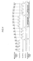
- FIG 1 A block diagram of a phase synchronization device according to a first exemplary embodiment of the present invention.
- FIG. 1 is a block diagram illustrating a configuration of a phase synchronization device 100 according to a first exemplary embodiment of the present invention.
- the phase synchronization device 100 is provided at the subsequent stage of a front-end section (not shown) of a communication receiver.
- the front-end section Upon reception of a signal that has been phase-modulated on the transmission side, the front-end section applies amplification, frequency conversion, filtering, etc., so as to put the reception signal into a condition suitable for demodulation and inputs the resultant signal to the phase synchronization device 100 as a reception signal 101.
- the front-end section includes an antenna, a low noise amplifier, a mixer, a communication band limiting filter, an interfering wave removal filter, and the like.
- the front-end section includes a reception input buffer designed in accordance with a transmission side output impedance and a transmission line characteristic impedance.
- the phase synchronization device 100 includes a sampling section 100A, a synchronization section 100B, and a clock generator 104.
- the sampling section 100A samples the reception signal that has passed through the front-end section to generate a quantized signal 108.
- the synchronization section 100B detects a reference phase synchronized with the phase of the quantized signal 108, in the digital signal region.
- the clock generator 104 supplies a common clock signal to the sampling section 100A and synchronization section 100B.
- the sampling section 100A includes a sampling filter 102 for converting the reception signal 101 which is a continuous-time signal into a discrete-time signal and a one-bit quantizer 107 for generating the quantized signal 108 representing a time-dependent change of the discrete-time signal.
- FIG. 2 illustrates a detailed configuration of the sampling section 100A.
- the reception signal 101 that has been input to the sampling filter 102 is then input to a two-system sample-and-hold circuit (103a and 103b).
- the sample and hold circuits 103a and 103b each have filter characteristics defined by a sampling clock of a frequency fs supplied from the clock generator 104.
- Sampling switches 105a and 105b in the sample and hold circuits 103a and 103b repeat ON/OFF operation according to clock signals "a" and "b" supplied thereto.
- Sampling capacitors 106a and 106b accumulate signals input thereto when switches 105a and 105b are tuned ON.
- Switches 105c1 and 105c2 are output switches operating according to a clock signal "c".
- the signals accumulated in the sampling capacitors 106a and 106b are output to the one-bit quantizer 107 when the switches 105c1 and 105c2 are tuned ON.
- the one-bit quantizer 107 generates, according to a clock signal supplied from the clock generator (104), the quantized signal 108 representing a time-dependent change of the discrete-time signal output from the sampling filter 102.
- the generated quantized signal 108 is output to the synchronization section 100B.
- the synchronization section 100B includes a phase difference detector 110, a low-pass filter 112, and a delay control circuit 114.
- the phase difference detector 110 outputs a phase difference signal 111 representing the phase difference between the quantized signal 108 output from the one-bit quantizer 107 and a reproduction demodulation clock 109 to be described later fed back from the delay control circuit 114.
- the low-pass filter 112 removes a high-frequency component which is noise for the phase difference signal 111 and outputs the resultant signal to the delay control circuit 114.
- the delay control circuit 114 generates a signal representing a time delay amount corresponding to the phase difference represented by the noise-removed phase difference signal 111, i.e., a filter output signal 113. Then, the reproduction demodulation clock 109 is fed back to the delay control circuit 114 at a timing set in consideration of the time delay amount.
- the reproduction demodulation clock corresponds to an inspection signal of the present invention.
- the reception signal 101 of a frequency f1 input to the sampling filter 102 is sampled by the sample and hold circuits 103a and 103b according to the clocks "a" and "b" each having a frequency fs0 and the sampled values are held by the sample and hold circuits 103a and 103b.
- the reception signal 101 is converted from a continuous-time signal into a discrete-time signal (step S1).
- FIG. 4 illustrates an example of the sampling performed by the sampling filter 102.
- the reception signal 101 is converted into discrete signals of A1 to A4 and A9 to A12 according to the clock "a" and discrete signals of B5 to B8 and B13 to B16 according to the clock "b".
- the values of A1 to A4 are held in the sampling capacitor 106a as an analog addition value (A1+A2+A3+A4), and values of A9 to A12 are held in the sampling capacitor 106a as an analog addition value (A9+A10+A11+A12).
- the values of B5 to B8 and values of B13 to B16 are held in the sampling capacitor 106b as analog addition values.
- the sampling filter 102 calculates the moving average of a block of four sampling points held in the sampling capacitors 106a and 106b. As a result of this calculation, a filter exhibiting low-pass characteristics is formed (step S2 of FIG. 3 ).
- the transfer function of the formed filter is represented by the following ⁇ Expression 1>.
- the switches 105c1 and 105c2 are tuned ON according to the clock "c" having a frequency (fs0)/4, the signal that has been subjected to the filtering with low-pass characteristics according to the ⁇ Expression 1> is output to the one-bit quantizer 107. More specifically, the average value of, e.g., A1+A2+A3+A4 is output from the sampling capacitor 106a, and average value of, e.g., B5+B6+B7+B8 is output from the sampling capacitor 106b.
- the one-bit quantizer 107 compares the two average values output from the sampling filter 102, that is, calculates the subtraction of two sampling points. As a result of the subtraction, a filter exhibiting high-pass characteristics is formed (step S3).
- the transfer function of the formed filter is represented by the following expression 2.
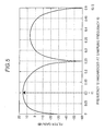
- a filter formed by the sampling filter 102 and one-bit quantizer 107 is a band-pass filter obtained by synthesizing the moving average low-pass filter represented by the ⁇ Expression 1> and subtractive high-pass filter represented by the ⁇ Expression 2>.
- the frequency characteristics of this filter is illustrated in FIG. 5 .
- band-pass characteristics as illustrated in FIG. 5 , noise included as a harmonic signal of a frequency 2 ⁇ f1, 3 ⁇ f1, and the like or noise such as thermal noise added when the signal passes through the front-end section of the precedent stage is removed.
- the characteristics of the band-pass filter may be changed in accordance with the degree of noise mixed into the reception signal (101).
- the filter characteristics represented by the ⁇ Expression 1> and ⁇ Expression 2> are characteristics of so-called a finite impulse response filter that does not have a process of feeding back a part of output as an input.
- a finite impulse response filter that does not have a process of feeding back a part of output as an input.
- a comparatively large number of calculation stages are required.
- an infinite impulse response filter that feeds back a part of output as an input may be used. This reduces the number of calculation stages.
- the filter characteristics In order to prevent intensity loss of the reception signal (101) caused due to use of the band-pass filter, it is desirable to set the filter characteristics such that the frequency f1 of the reception signal (101) is located at the maximum gain point (denoted by a broken arrow) in the frequency characteristics of FIG. 5 .
- the quantized signal 108 output from the one-bit quantizer 107 represents the time rate of change in the interval 1/(fs0/4) in the case where the reception signal 101 is regarded as a sine wave.
- the one-bit quantizer 107 outputs a signal of "1". This signal represents that a change in the reception signal on the time axis has a positive slope (step S5).
- the one-bit quantizer 107 In the reverse case (No in step S4), the one-bit quantizer 107 outputs a signal of "0" representing that a change in the reception signal on the time axis has a negative slope (step S6). As described above, the one-bit quantizer 107 of the present exemplary embodiment simply represents the time-dependent change of the reception signal waveform with binary values of "0" and "1".
- the linear distortion of the reception signal 101 is removed to some extent by the filter formed in the sampling section 100A. Therefore, in the synchronization section 100B of the subsequent stage, it is sufficient to obtain binary level information as information representing the time-dependent change of the reception signal 101. Further, the use of the one-bit quantizer 107 simplifies the circuit configuration, thereby enabling a reduction in the circuit scale.
- the operation shifts to the operation of combining the phase of the quantized signal 108 and phase of the inspection signal (reproduction demodulation clock 109) for phase synchronization.
- the phase difference detector 110 detects the time difference between the rising edge of the quantized signal 108 and rising edge of the reproduction demodulation clock 109 serving as the inspection signal and outputs the detected time difference as the phase difference signal 111 (step S7 of FIG. 3 ).
- NOT gates 110a and 110c, and NAND gate 110b constituted as shown in FIG. 6 are used as The phase difference detector 110.
- the phase difference signal 111 represents the time difference between the rising edges of the reproduction demodulation clock 109 and quantized signal 108. Actually, however, the phase difference signal 111 includes high-frequency noise that has been mixed along the way to the phase difference detector 110. Thus, the low-pass filter 112, which is a digital filter, is used to remove the high frequency noise (step S8). This facilitates extraction of the time difference information from the phase difference signal 111.
- the low-pass filter 112 may be constituted by delay flip-flop circuits (DFF) 112a and 112b operating according to a filter clock 104A supplied from the clock generator 104, and an XOR gate 112c.
- DFF delay flip-flop circuits
- FIG. 7 illustrates the waveform of the phase difference signal 111 corresponding to the phase difference between the quantized signal 108 and reproduction demodulation clock 109 and waveform of the filter output signal 113 generated according to the filter clock 104A.
- the low-pass filter 112 outputs, as the filter output signal 113, the moving average of the phase difference signal 111 at three consecutive timings which is based on the filter clock 104A.
- the characteristics of the low-pass filter 112 are appropriately set in accordance with noise that can be included in the phase difference signal 111. Since the low-pass filter 112 is a digital filter ( FIG. 6 ) constituted by only the logic gates as described above, the characteristics can comparatively easily be controlled.
- the phase difference signal 111 is subjected to removal of the high-frequency noise by the low-pass filter 112 and then input to the delay control circuit 114 as the filter output signal 113.
- the delay control circuit 114 determines whether the input filter output signal 113 exhibits the same phase as those of the quantized signal 108 and reproduction demodulation clock 109. While the reproduction demodulation clock 109 has not yet been synchronized with the quantized signal 108, e.g., at the starting point of the synchronization processing, the filer output signal 113 does not exhibit the same phase (No in step S9 of FIG. 3 ).
- the delay control circuit 114 generates a control code corresponding to the current phase difference so as to make the filter output signal 113 exhibit the same phase (step S10) and feeds back the reproduction demodulation clock 109 serving as the inspection signal to the phase difference detector 110 at a delayed timing based on the control code (step S11).
- a digital phase adjustment circuit 114c is a digital circuit that discretely controls the rising edge position of the reproduction demodulation clock 109.
- the digital phase adjustment circuit 114c identifies the delay amount ([Deg.]) to be added to the output timing of the reproduction demodulation clock 109, based on a control code 114b (binary number) output from a decoder 114a.
- the decoder 114a generates the control code 114b corresponding to the phase difference represented by the filter output signal 113 output from the low-pass filter 112.
- the pulse width of the filter output signal 113 corresponds to the time difference between the rising edge of the quantized signal 108 and rising edge of the reproduction demodulation clock 109.
- the filter output signal 113 exhibits a certain amount of phase difference until the phase synchronization is established.
- the above operation of the delay control circuit 114 is the operation of feeding back the reproduction demodulation clock 109 to the phase difference detector 110 at the timing set in consideration of a delay amount corresponding to the current phase difference. This operation is repetitively performed so as to make the phase difference represented by the filter output signal 113 converge to 0.
- the delay control circuit 114 recognizes that the phase synchronization between the reception signal 101 and reproduction demodulation clock 109 has been established (step S12).
- the phase of the reproduction demodulation clock 109 at this time point corresponds to the reference phase to be detected in the synchronization section 10B.
- the one-bit quantizer 107 demodulates the reception signal using the detected reference phase, whereby data can be reproduced properly.
- the phase of a carrier wave of a reception signal always fluctuates due to mixing of various noise components.
- the convergence time of the feedback loop is comparatively short.
- the convergence time tends to be long.
- the phase-shift that fluctuates with a long period causes degradation of bit error rate particularly in the case of communication with a large amount of data.
- the present exemplary embodiment it is possible to eliminate the need of providing a high resolution power/high sampling rate A/D converter which has been required in a conventional technique in which the reference phase is detected in the digital signal region. This enables a reduction in the circuit scale and power consumption.
- filtering for noise removal is performed in the sampling section 100A of the precedent stage that operates according to the same clock as the synchronization section 100B ( FIG. 5 ). That is, in the sampling section 100A of the precedent stage that operates according to the same clock as the synchronization section 100B, a certain amount of noise has already been removed from the quantized signal 108 to be input to the synchronization section 100B, which prevents the convergence time of the subsequent loop processing in the synchronization section 100B from being increased.
- sampling section 100A can be utilized not only for the phase synchronization processing described in the above exemplary embodiment but also for subsequent data demodulation processing. This configuration contributes to a reduction of the size of the entire reception circuit.
- FIG. 9 illustrates a configuration of a second exemplary embodiment of the present invention.
- the same reference numerals are given to those components that are the same as the corresponding components of the first embodiment ( FIG. 1 ).
- a phase synchronization device 200 of the present exemplary embodiment includes a sampling section 200A, the synchronization section 100B, the clock generator 104, a multi-phase generator 215, and a phase compensator 216.
- the multi-phase generator 215 converts a clock signal to be supplied from the clock generator 104 to a sampling switch of a sampling filter 202 into multi-phase clock signals.
- the phase compensator 216 compensates the correlation skews of the multi-phase clock signals to be input to the sampling filter 202, that is, compensates the phase variation between the multi-phase clock signals.
- FIG. 10 illustrates a part of a configuration of the sampling filter 202 according to the present exemplary embodiment.
- the configuration illustrated relates to a clock a which is one of clock signals output from the clock generator (104).
- the sampling filter 202 has a sample and hold circuit 203a receiving clock a1 to a4 obtained by multi-phasing of the clock "a".
- the sampling filter 202 has sample and hold circuits corresponding to the number of multi-phases of clocks other than the clock a.
- the basic configuration of the sample and hold circuit 203a corresponds to the configuration of the sample and hold circuit 103a ( FIG. 2 ) according to the above first exemplary embodiment. That is, the sample and hold circuit 203 a has sampling switches 105a1 to 105a4 that turn ON/OFF according to the clocks a1 to a4 and accumulates discrete-time signals of the reception signal 101 in respective sampling capacitors at ON time of the sampling switches.
- phase synchronization device 200 having the configuration described above will be described.
- the operation of the synchronization section 100B according to the present exemplary embodiment is the same as that of the first exemplary embodiment, and the description thereof will be omitted.
- a part of the operation of the sampling section 200A different from that of the sampling section 100A of the first exemplary embodiment will mainly be described.
- the multi-phase generator 215 divides the phase of the clock "a" input from the clock generator 104 to generate clocks a1 to a4 of four phases and outputs the generated clocks to the phase compensator 216.
- the phase compensator 216 adjusts the correlation skews of the clocks a1 to a4 and sequentially inputs the resultant clocks to the sample and hold circuit 203a. More concretely, as illustrated in FIG. 10 , the clock a1 is input to the switch 105a1 of the sample and hold circuit 203a, clock a2 is input to the switch 105a2, clock a3 is input to the switch 105a3, and clock a4 is input to the switch 105a4.
- FIG. 11 illustrates the timing relationship between the clocks a1 to a4 and clock "c".
- consecutive sample values like A1 to A4 FIG. 4
- the multi-phased clocks a1 to a4 are used to acquire consecutive sample values based on the plurality of clocks.
- the clock a1 is used to acquire A1
- clock a2 is used to acquire A2
- clock a3 is used to acquire A3
- clock a4 is used to acquire A4.
- the sampling filter 202 adds the acquired sample values (A1+A2+A3+A4) at the timing of the clock "c" and outputs the average value of the added value to the one-bit quantizer 107. This operation is the same as that of the above first exemplary embodiment.
- the clock signal for obtaining consecutive sample values is multi-phased, so that the sampling frequency can easily be increased. This is useful in, e.g., an environment where it is difficult to sufficiently increase the sampling frequency.
- the present invention is not limited to the above exemplary embodiments and may appropriately be modified within the scope of the claims of the invention.
- the low-pass filter 112 is provided at the subsequent stage of the phase difference detector 110 in order to remove high-frequency noise included in the phase difference signal 111 in the above exemplary embodiments; however, in the case where the noise can sufficiently be removed by the filtering ( FIG. 5 ) in the sampling section 100A, the low-pass filter 112 need not be provided in the synchronization section 100B.
- the processing time in the synchronization section 100B can be reduced by the amount corresponding to the omission of the filtering processing.
- the single clock generator (104) is used in order to supply a common clock signal to the respective circuits in the phase synchronization device, a plurality of clock generators may be used. In this case, clock signals from the respective generators are previously synchronized with one another before being supplied.
Landscapes
- Engineering & Computer Science (AREA)
- Computer Networks & Wireless Communication (AREA)
- Signal Processing (AREA)
- Digital Transmission Methods That Use Modulated Carrier Waves (AREA)
- Synchronisation In Digital Transmission Systems (AREA)
- Circuits Of Receivers In General (AREA)
Applications Claiming Priority (2)
| Application Number | Priority Date | Filing Date | Title |
|---|---|---|---|
| JP2008023779 | 2008-02-04 | ||
| PCT/JP2009/051406 WO2009098989A1 (fr) | 2008-02-04 | 2009-01-29 | Dispositif de synchronisation de phase et procédé de synchronisation de phase |
Publications (2)
| Publication Number | Publication Date |
|---|---|
| EP2249534A1 true EP2249534A1 (fr) | 2010-11-10 |
| EP2249534A4 EP2249534A4 (fr) | 2016-05-18 |
Family
ID=40952065
Family Applications (1)
| Application Number | Title | Priority Date | Filing Date |
|---|---|---|---|
| EP09707566.7A Withdrawn EP2249534A4 (fr) | 2008-02-04 | 2009-01-29 | Dispositif de synchronisation de phase et procédé de synchronisation de phase |
Country Status (4)
| Country | Link |
|---|---|
| US (1) | US8125258B2 (fr) |
| EP (1) | EP2249534A4 (fr) |
| JP (1) | JP5354293B2 (fr) |
| WO (1) | WO2009098989A1 (fr) |
Families Citing this family (9)
| Publication number | Priority date | Publication date | Assignee | Title |
|---|---|---|---|---|
| EP2299588B1 (fr) * | 2009-09-11 | 2012-12-19 | Stichting IMEC Nederland | Récepteur avec performance de bruit améliorée |
| WO2016061781A1 (fr) * | 2014-10-23 | 2016-04-28 | Lattice Semiconductor Corporation | Boucle à verrouillage de phase (pll) à fonctionnalité empêchant un verrouillage sous-harmonique |
| KR102022377B1 (ko) * | 2017-12-18 | 2019-09-18 | 주식회사 포인투테크놀로지 | 위상 동기화 장치 |
| WO2019124721A1 (fr) * | 2017-12-18 | 2019-06-27 | 주식회사 포인투테크놀로지 | Dispositif de synchronisation de phase |
| US10746814B2 (en) * | 2018-06-21 | 2020-08-18 | Allegro Microsystems, Llc | Diagnostic methods and apparatus for magnetic field sensors |
| JP7174271B2 (ja) * | 2018-07-10 | 2022-11-17 | 株式会社ソシオネクスト | 位相同期回路、送受信回路及び集積回路 |
| US11561257B2 (en) | 2020-12-22 | 2023-01-24 | Allegro Microsystems, Llc | Signal path monitor |
| US20260081813A1 (en) * | 2024-09-16 | 2026-03-19 | Infineon Technologies Ag | Demodulator circuit |
| CN120352870B (zh) * | 2025-06-23 | 2025-09-19 | 中国科学院空天信息创新研究院 | 一种基于频率扫描的双基sar相位同步方法及装置 |
Family Cites Families (15)
| Publication number | Priority date | Publication date | Assignee | Title |
|---|---|---|---|---|
| US4233565A (en) * | 1979-06-29 | 1980-11-11 | Motorola, Inc. | Method and apparatus for a PSK signal detector |
| EP0467712B1 (fr) * | 1990-07-20 | 1998-04-29 | Nec Corporation | Démodulateur de phase pour signaux modulés en sauts de phase |
| JP2841935B2 (ja) | 1990-07-20 | 1998-12-24 | 日本電気株式会社 | 位相復調器 |
| JP2885254B2 (ja) * | 1991-10-16 | 1999-04-19 | 日本電気株式会社 | ボータイミング抽出回路 |
| JPH0630063A (ja) * | 1992-07-08 | 1994-02-04 | Sanyo Electric Co Ltd | デジタル復調器 |
| JP2795585B2 (ja) | 1992-08-19 | 1998-09-10 | ユニデン株式会社 | 選択呼出し受信機のフィルタ回路 |
| JPH09130443A (ja) * | 1995-10-31 | 1997-05-16 | Toshiba Corp | ディジタル復調装置 |
| JPH09224063A (ja) * | 1996-02-16 | 1997-08-26 | Nippon Telegr & Teleph Corp <Ntt> | クロック再生回路 |
| JP3628463B2 (ja) | 1996-12-26 | 2005-03-09 | 松下電器産業株式会社 | デルタシグマ型a/d変換器 |
| JP2002094585A (ja) | 2000-09-12 | 2002-03-29 | Sony Corp | 受信装置、フィルタ回路制御装置およびそれらの方法 |
| JP2002124999A (ja) | 2000-10-16 | 2002-04-26 | Ee O R:Kk | Psk同調確認方法及びpsk同調確認装置 |
| JP2006041580A (ja) | 2004-07-22 | 2006-02-09 | Renesas Technology Corp | 通信用半導体集積回路 |
| EP1806891A4 (fr) | 2004-10-27 | 2012-09-26 | Nec Corp | Récepteur numérique sans fil |
| JP2007174620A (ja) * | 2005-11-25 | 2007-07-05 | Seiko Epson Corp | Psk受信機、psk復調回路、通信装置、および、psk受信方法 |
| JP5046622B2 (ja) | 2005-12-13 | 2012-10-10 | パナソニック株式会社 | サンプリングフィルタ装置 |
-
2009
- 2009-01-29 EP EP09707566.7A patent/EP2249534A4/fr not_active Withdrawn
- 2009-01-29 JP JP2009552448A patent/JP5354293B2/ja not_active Expired - Fee Related
- 2009-01-29 WO PCT/JP2009/051406 patent/WO2009098989A1/fr not_active Ceased
- 2009-01-29 US US12/865,192 patent/US8125258B2/en active Active
Non-Patent Citations (1)
| Title |
|---|
| See references of WO2009098989A1 * |
Also Published As
| Publication number | Publication date |
|---|---|
| JP5354293B2 (ja) | 2013-11-27 |
| EP2249534A4 (fr) | 2016-05-18 |
| JPWO2009098989A1 (ja) | 2011-05-26 |
| US8125258B2 (en) | 2012-02-28 |
| US20100308879A1 (en) | 2010-12-09 |
| WO2009098989A1 (fr) | 2009-08-13 |
Similar Documents
| Publication | Publication Date | Title |
|---|---|---|
| US8125258B2 (en) | Phase synchronization device and phase synchronization method | |
| JP4979413B2 (ja) | パルス無線受信装置 | |
| US20070140382A1 (en) | Bandpass sampling receiver and the sampling method | |
| US6996193B2 (en) | Timing error detection circuit, demodulation circuit and methods thereof | |
| EP0805560A2 (fr) | Circuit d'asservissement de phase numérique et procédé d'initalisation | |
| US20110043693A1 (en) | Synchronous control circuit and video display device | |
| CN111492533B (zh) | 相位同步装置 | |
| WO2005055449A1 (fr) | Recepteur a echantillonnage en bande passante et procede d'echantillonnage correspondant | |
| US8861648B2 (en) | Receiving device and demodulation device | |
| KR100505669B1 (ko) | 디지털 텔레비전 수신 시스템의 복조 회로 및 복조 방법 | |
| CN101005480A (zh) | 解调电路和解调方法 | |
| JP4463063B2 (ja) | 復調回路及び復調方法 | |
| JPH118659A (ja) | クロックタイミング再生方法および回路 | |
| JP2000049877A (ja) | クロックタイミング再生回路 | |
| JP4637661B2 (ja) | 変調信号の復調装置 | |
| KR960000542B1 (ko) | 디지탈 무선 통신 시스템에서 동기 신호를 이용한 프레임 타이밍신호 추출방법 및 시스템 | |
| KR100289404B1 (ko) | 국소대칭강제파형부를 이용한 패턴지터를 줄이는 장치 및 방법 | |
| JP2005303846A (ja) | ディジタル復調器 | |
| KR19980077667A (ko) | 심볼 타이밍 복구장치 | |
| EP1578076A1 (fr) | Dispositif de detection de la position d'un symbole, et procede correspondant | |
| JP5269751B2 (ja) | 復調装置 | |
| JP2016058979A (ja) | 復調装置および無線装置 | |
| JP2002111763A (ja) | デジタル直交変調信号の復調装置及び方法 | |
| JP2001024562A (ja) | デジタルpll装置およびシンボル同期装置 | |
| JP2006157652A (ja) | 受信装置 |
Legal Events
| Date | Code | Title | Description |
|---|---|---|---|
| PUAI | Public reference made under article 153(3) epc to a published international application that has entered the european phase |
Free format text: ORIGINAL CODE: 0009012 |
|
| 17P | Request for examination filed |
Effective date: 20100729 |
|
| AK | Designated contracting states |
Kind code of ref document: A1 Designated state(s): AT BE BG CH CY CZ DE DK EE ES FI FR GB GR HR HU IE IS IT LI LT LU LV MC MK MT NL NO PL PT RO SE SI SK TR |
|
| AX | Request for extension of the european patent |
Extension state: AL BA RS |
|
| DAX | Request for extension of the european patent (deleted) | ||
| RA4 | Supplementary search report drawn up and despatched (corrected) |
Effective date: 20160419 |
|
| RIC1 | Information provided on ipc code assigned before grant |
Ipc: H04L 27/227 20060101AFI20160413BHEP Ipc: H04L 7/033 20060101ALI20160413BHEP |
|
| STAA | Information on the status of an ep patent application or granted ep patent |
Free format text: STATUS: THE APPLICATION HAS BEEN WITHDRAWN |
|
| 18W | Application withdrawn |
Effective date: 20160926 |