EP2249621B1 - Zur Verwendung in einem Dimmer angepasste LED-Dimmervorrichtung - Google Patents
Zur Verwendung in einem Dimmer angepasste LED-Dimmervorrichtung Download PDFInfo
- Publication number
- EP2249621B1 EP2249621B1 EP09159349.1A EP09159349A EP2249621B1 EP 2249621 B1 EP2249621 B1 EP 2249621B1 EP 09159349 A EP09159349 A EP 09159349A EP 2249621 B1 EP2249621 B1 EP 2249621B1
- Authority
- EP
- European Patent Office
- Prior art keywords
- voltage
- dimmer
- led
- detection circuit
- transformer
- Prior art date
- Legal status (The legal status is an assumption and is not a legal conclusion. Google has not performed a legal analysis and makes no representation as to the accuracy of the status listed.)
- Not-in-force
Links
- 238000001514 detection method Methods 0.000 claims description 15
- 230000005669 field effect Effects 0.000 claims description 3
- 229910044991 metal oxide Inorganic materials 0.000 claims description 3
- 150000004706 metal oxides Chemical class 0.000 claims description 3
- 239000004065 semiconductor Substances 0.000 claims description 3
- 238000001914 filtration Methods 0.000 claims description 2
- WFKWXMTUELFFGS-UHFFFAOYSA-N tungsten Chemical compound [W] WFKWXMTUELFFGS-UHFFFAOYSA-N 0.000 description 11
- 229910052721 tungsten Inorganic materials 0.000 description 11
- 239000010937 tungsten Substances 0.000 description 11
- 230000001960 triggered effect Effects 0.000 description 2
- 238000005516 engineering process Methods 0.000 description 1
- 238000012986 modification Methods 0.000 description 1
- 230000004048 modification Effects 0.000 description 1
- 230000001131 transforming effect Effects 0.000 description 1
Images


Classifications
-
- H—ELECTRICITY
- H05—ELECTRIC TECHNIQUES NOT OTHERWISE PROVIDED FOR
- H05B—ELECTRIC HEATING; ELECTRIC LIGHT SOURCES NOT OTHERWISE PROVIDED FOR; CIRCUIT ARRANGEMENTS FOR ELECTRIC LIGHT SOURCES, IN GENERAL
- H05B45/00—Circuit arrangements for operating light-emitting diodes [LED]
- H05B45/30—Driver circuits
- H05B45/37—Converter circuits
- H05B45/3725—Switched mode power supply [SMPS]
- H05B45/382—Switched mode power supply [SMPS] with galvanic isolation between input and output
-
- H—ELECTRICITY
- H05—ELECTRIC TECHNIQUES NOT OTHERWISE PROVIDED FOR
- H05B—ELECTRIC HEATING; ELECTRIC LIGHT SOURCES NOT OTHERWISE PROVIDED FOR; CIRCUIT ARRANGEMENTS FOR ELECTRIC LIGHT SOURCES, IN GENERAL
- H05B45/00—Circuit arrangements for operating light-emitting diodes [LED]
- H05B45/30—Driver circuits
- H05B45/37—Converter circuits
- H05B45/3725—Switched mode power supply [SMPS]
- H05B45/385—Switched mode power supply [SMPS] using flyback topology
-
- H—ELECTRICITY
- H05—ELECTRIC TECHNIQUES NOT OTHERWISE PROVIDED FOR
- H05B—ELECTRIC HEATING; ELECTRIC LIGHT SOURCES NOT OTHERWISE PROVIDED FOR; CIRCUIT ARRANGEMENTS FOR ELECTRIC LIGHT SOURCES, IN GENERAL
- H05B45/00—Circuit arrangements for operating light-emitting diodes [LED]
- H05B45/30—Driver circuits
- H05B45/355—Power factor correction [PFC]; Reactive power compensation
-
- H—ELECTRICITY
- H05—ELECTRIC TECHNIQUES NOT OTHERWISE PROVIDED FOR
- H05B—ELECTRIC HEATING; ELECTRIC LIGHT SOURCES NOT OTHERWISE PROVIDED FOR; CIRCUIT ARRANGEMENTS FOR ELECTRIC LIGHT SOURCES, IN GENERAL
- H05B45/00—Circuit arrangements for operating light-emitting diodes [LED]
- H05B45/30—Driver circuits
- H05B45/37—Converter circuits
- H05B45/3725—Switched mode power supply [SMPS]
- H05B45/38—Switched mode power supply [SMPS] using boost topology
Definitions
- the present invention relates to a dimmer device, and more particularly pertains to a LED dimmer device adapted for use in dimmer.
- Si-controlled dimmer and electro-transistor dimmer can adjust brightness of tungsten lamp.
- on-time of dimmer 5 is determined by charging time of capacitance 9 of circuit, and therefore change conduction angle of sinusoidal alternating current non-sinusoidal waveforms, and thus change current of the tungsten lamp 10 so as to adjust brightness, which is defined as leading edge technology.
- dimmer 5 is connected with tungsten lamp 10 in series. Current passes through fuse 1, inductance 2, Potentiometer 7, resistance 8, capacitance 9, and tungsten lamp 10 to form a charging loop of charging capacitance 9.
- the charging time of the capacitance 9 is determined by resistance of the potentiometer 7.
- the capacitance 9 When charging of the capacitance 9 is finished after a predetermined time, the capacitance 9 triggers control end of the dimmer 5 via trigger diode 6 to make dimmer 5 conductive. Because the tungsten lamp 10 is resistance load, a voltage waveform 1 is consistent with current waveform 3 (referring to FIG. 2 ) after edge of dimmer, and the on-time is same as off-time. Therefore, the adjusting of brightness of the tungsten lamp 10 is achieved.
- LED is energy-saving and new lamp.
- the power of LED is much smaller than tungsten lamp.
- LED is a low-voltage direct current element.
- LED lamp need to be equipped with a LED driving power supply so as to be drived to illuminate.
- LED driving-switch power supply is capacitive load and is not equipped with dimmer control circuit.
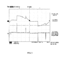
- the on-time of the dimmer 5 is shorter than that of voltage (referring to FIG. 3 ).
- there is no current passing through the dimmer 5 there is voltage existed between the resistance 7 and the capacitance 9. This voltage charges for the capacitance 9.
- the dimmer 5 When charging for a predetermined time, the dimmer 5 is triggered, the dimmer 5 is in on-time twice in a half-period. LED lamp flashes frequently because of intermittence of input of driving-switch power supply. Therefore, the dimmer cannot adjust brightness of LED lamp with Internal/Extemal Auto-switch
- a dimmer device adapted for use in dimmer is desired to overcome the above-described shortcomings.
- US-A-2005/0231133 in its figures 8-10 shows a conventional light source power supply, which employs a power factor correction apparatus between the rectifier and the DC-DC converter for adjusting the waveform and phase of the input voltage.
- the DC-DC converter of the power supply has a feedback-control loop as a power supply controller to receive the converter's output voltage and provide a control signal to a switch so as to adjust the amount of energy transferred across the transformer of the converter in a given time period.
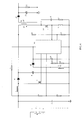
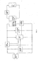
- the LED dimmer device includes rectifier, voltage boost device, pre-voltage detection circuit and after-voltage detection circuit adapted for detecting voltage, master chip adapted for driving circuit and elements to work, elementary transformer and secondary transformer adapter for changing voltage, secondary rectifier adapted for rectifying and secondary filter capacitance circuit adapter for filtering, and secondary switch.
- the rectifier is adapted for transforming alternating current into direct current.
- the voltage boost device includes a metal oxide semiconductor field effect transistor used to make dimmer entering into a normal phase-cutting state.
- the master chip includes integrated comparing element used to compare voltage.
- the secondary switch is used to drive transformer primary and secondary circuits, secondary rectifier, secondary filter capacitance circuit so as to drive LED light source to illuminate.
- the voltage booster device is adapted for enabling on-time current and on-time voltage of dimmer being in same phase mode, and having a relative lower peak value of current.
- the voltage of the pre-voltage detection circuit changes correspondingly, which acts as standard voltage to control brightness changing and is inputted to the master chip to control frequency and duty-cycle of secondary switch, then the primary and secondary circuits of transformer, secondary rectifier and secondary filter circuit are driven so as to drive LED light source to illuminate.
- the dimmer is any one of Si-controlled dimmer and electro-transistor dimmer.
- the number of the LED light source is one or more, and the LED light source is single color or multi-color.
- Si-controlled dimmer and electro-transistor dimmer may adjust brightness of LED light source such that environment friendly LED is more widely applied.
- the dimmer device has good the brightness adjusting efficiency.
- mains supply voltage is transformed into direct-current voltage via primary rectifier 1 and filter capacitance 2.
- the start-up resistance 9 firstly charges the master chip 10 so as to drive voltage boost device 5, 6, 7 to work.
- the voltage respectively detected by pre-voltage detection circuit 3, 4 and after-voltage detection circuit 11, 12 are simultaneously inputted to integrated comparator in the master chip 10 to compare, and then duty-cycle of metal oxide semiconductor field effect transistor (MOSFET) 7 of the step-up is adjusted to ensure that the voltage of step-up filter capacitance 8 is higher 30 volt-ampere than that of the filter capacitance 2.
- MOSFET metal oxide semiconductor field effect transistor
- the peak value current of the adapter is relative low and has the same on-time as the voltage waveform. Furthermore, the power factor can be over 0.8.
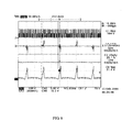
- switch tubes of step-up circuit is always in high frequency switch working state. The charge path of trigger circuit of the adapter is maintained, the adapter can be triggered again and works normally, which can be seen from waveform shown in FIG. 6 and FIG. 7 .
- the secondary switch 14 is driven by the master chip 10 to work.
- the pre-voltage detection circuit 3, 4 can detect change of voltage, which is also detection voltage of adapting information, and which is inputted to the master chip 10.
- Changing the duty-cycle of the secondary switch 14 adapts elementary charging current of the transformer.
- the secondary switch 14 is turned off, energy of transformer obtained by charging discharges to transformer secondary circuit 23. After acted by the secondary rectifier 24 and the secondary filter capacitance 25, the LED is driven to illuminate. Therefore, the brightness and driving current of the LED is controlled by the adapter such that the Si-controlled dimmer and electro-transistor dimmer can adjust the LED light source.
- FIG. 6 shows a schematic view of voltage and current waveform of a dimmer device adapted for use in dimmer according to a preferred embodiment according to the present invention.
- 1 indicates waveform rectified by electro-transistor dimmer, and the Si-controlled is adjusted to a lowest controlling angle, and the voltage thereof is 164 VDC.
- 2 indicates voltage waveform of the capacitance after step-up, and maximum of voltage is 210 VDC.
- 3 indicates alternating current waveform, in which current and voltage are in same mode and in same on-time. Maximum of current is 360 MA. 4 indicates driving waveform of MOSFET, of which frequency is 63 KHZ, and of which duty-cycle is 32%.
- FIG. 7 shows a schematic view of voltage and current waveform of a dimmer device adapted for use in dimmer according to a preferred embodiment according to the present invention.
- 1 indicates waveform rectified by Si-controlled dimmer, and the Si-controlled is adjusted to a lowest controlling angle, and the voltage thereof is 184 VDC.
- 2 indicates voltage waveform of the capacitance after step-up, and maximum of voltage is 250 VDC.
- 3 indicates alternating current waveform, in which current and voltage are in same phase mode and in same on-time. Maximum of current is 300 mA.
- 4 indicates driving waveform of MOSFET, of which frequency is 63 KHZ, and of which duty-cycle is 25%.
Landscapes
- Circuit Arrangement For Electric Light Sources In General (AREA)
Claims (6)
- Zum Betrieb mit einem Phasenabschnittsdimmer abgestimmte LED-Dimmervorrichtung, welche umfasst:einen für die Umwandlung von Wechselstrom zu Gleichstrom angepassten Primärgleichrichter (1);einen Spannungserhöher (5-7), welcher einen Transistor (7) beinhaltet, abgestimmt, um den Dimmer in einen normalen Phasenanschnitt-Betrieb kommen zu lassen;eine Eingangsspannungs-Detektorschaltung (3, 4) sowie eine Nachspannungs-Detektorschaltung (11, 12), abgestimmt für das Erkennen einer Spannung nach dem Primärgleichrichter beziehungsweise einer Spannung nach dem Spannungserhöher;einen für die Ansteuerung der Stromkreise und Elemente der Vorrichtung angepassten Masterchip (10), wobei der Masterchip einen integrierten Komparator beinhaltet, der ausgelegt ist auf das Abgleichen von Spannungen;einen Transformator, der einen Primärkreis (13) und einen Sekundärkreis (23) beinhaltet, ausgelegt für eine Spannungsänderung, wobei der Primärkreis (13) verbunden ist mit dem Ausgang des Spannungserhöhers (5-7);einen für die Gleichrichtung des Ausgangsstroms des besagten Transformators angepassten Sekundärgleichrichter (24);einen für das Filtern des Ausgangsstroms des Transformators angepassten Sekundärfilter (25, 26);
undeinen Sekundärschalter (14), der ausgelegt ist auf den Betrieb des besagten Primär- und Sekundärkreises des Transformators, des Sekundärgleichrichters und des Sekundärfilters, sodass die LED-Lichtquelle zum Leuchten gebracht werden kann,
dadurch gekennzeichnet,dass besagter Transistor (7) des Spannungserhöhers (5-7) ein Metall-Oxid-Halbleiter-Feldeffekttransistor ist, unddass besagter Masterchip (10) ausgerichtet ist auf den Betrieb des Sekundärschalters (14), basierend auf der durch die Eingangsspannungs-Detektorschaltung (3, 4) erkannten Spannung. - Die LED-Dimmervorrichtung nach Anspruch 1, wobei der Spannungserhöher so ausgelegt ist, dass er bewirkt, dass Laststrom und Lastspannung des Dimmers die gleiche Phase haben, sowie dass der Spitzenwert des Stroms im Vergleich geringer ist.
- Die LED-Dimmervorrichtung nach Anspruch 2, wobei nach Gleichrichtung des Wechselstroms die Vorrichtung ausgelegt ist auf das zeitgleiche Einspeisen der durch die Eingangsspannungs-Detektorschaltung erkannten Spannung sowie der durch die Detektorschaltung für die Spannung nach dem Spannungserhöher gemessenen Spannung in besagten integrierten Komparator des Masterchip, um dadurch Frequenz und Tastverhältnis des Spannungserhöhers so zu steuern, dass die Differenz zwischen der hochtransformierten Spannung und der elementar gleichgerichteten Spannung bei 30 Volt gehalten wird.
- Die LED-Dimmervorrichtung nach Anspruch 3, wobei das Gerät ausgelegt ist auf die Änderung des Einschaltwinkels der Wechselspannung des Phasenanschnittdimmers, sodass sich die Spannung an der Eingangsspannungs-Detektorschaltung entsprechend ändert, welche als Basisspannung für eine Helligkeitsänderung der LED-Lichtquelle dient und angepasst wird, um vom Masterchip eingelesen zu werden, um Frequenz und Tastverhältnis des Sekundärschalters zu steuern, sodass der Transformator, der Sekundärgleichrichter und der Sekundärfilter in einer Weise angesteuert werden, dass die LED-Lichtquelle zum Leuchten gebracht wird.
- Dimmer, der eine LED-Dimmervorrichtung nach Anspruch 1 beinhaltet, wobei der Dimmer ein Si-gesteuerter Dimmer oder ein Elektrotransistor-Dimmer ist.
- LED-Anordnung die eine LED-Dimmervorrichtung nach Anspruch 1 beinhaltet, wobei die LED-Lichtquelle eine oder mehrere LEDs aufweist, und die LED-Lichtquelle einfarbig oder mit Farbwechsel ist.
Priority Applications (1)
| Application Number | Priority Date | Filing Date | Title |
|---|---|---|---|
| EP09159349.1A EP2249621B1 (de) | 2009-05-04 | 2009-05-04 | Zur Verwendung in einem Dimmer angepasste LED-Dimmervorrichtung |
Applications Claiming Priority (1)
| Application Number | Priority Date | Filing Date | Title |
|---|---|---|---|
| EP09159349.1A EP2249621B1 (de) | 2009-05-04 | 2009-05-04 | Zur Verwendung in einem Dimmer angepasste LED-Dimmervorrichtung |
Publications (2)
| Publication Number | Publication Date |
|---|---|
| EP2249621A1 EP2249621A1 (de) | 2010-11-10 |
| EP2249621B1 true EP2249621B1 (de) | 2014-04-30 |
Family
ID=40941658
Family Applications (1)
| Application Number | Title | Priority Date | Filing Date |
|---|---|---|---|
| EP09159349.1A Not-in-force EP2249621B1 (de) | 2009-05-04 | 2009-05-04 | Zur Verwendung in einem Dimmer angepasste LED-Dimmervorrichtung |
Country Status (1)
| Country | Link |
|---|---|
| EP (1) | EP2249621B1 (de) |
Families Citing this family (2)
| Publication number | Priority date | Publication date | Assignee | Title |
|---|---|---|---|---|
| GB2507308A (en) * | 2012-10-25 | 2014-04-30 | Spled Ltd | LED module driver |
| CN108289354A (zh) * | 2018-02-02 | 2018-07-17 | Tcl-罗格朗国际电工(惠州)有限公司 | 调光电路及电位器 |
Family Cites Families (3)
| Publication number | Priority date | Publication date | Assignee | Title |
|---|---|---|---|---|
| US6956336B2 (en) * | 2002-07-22 | 2005-10-18 | International Rectifier Corporation | Single chip ballast control with power factor correction |
| DK3589081T3 (da) | 2004-03-15 | 2024-03-18 | Signify North America Corp | Effektstyringfremgangsmåder og -apparat |
| KR100727354B1 (ko) * | 2005-11-09 | 2007-06-13 | 주식회사 유양정보통신 | 발광 다이오드 정전류 펄스폭 변조 구동 회로 |
-
2009
- 2009-05-04 EP EP09159349.1A patent/EP2249621B1/de not_active Not-in-force
Also Published As
| Publication number | Publication date |
|---|---|
| EP2249621A1 (de) | 2010-11-10 |
Similar Documents
| Publication | Publication Date | Title |
|---|---|---|
| US8139378B2 (en) | LED dimmer device adapted for use in dimmer | |
| US8736194B2 (en) | LED dimmer circuit | |
| CN100482015C (zh) | 照明用的低压电源电路、低压电源输出方法以及照明装置 | |
| CN101505568B (zh) | 一种适用于调光器的led调光装置 | |
| US9271347B2 (en) | TRIAC dimmable LED driver circuit | |
| CN102412709B (zh) | 开关电源装置以及可调节电源系统 | |
| CN102099621B (zh) | 发光二极管灯 | |
| US8872444B2 (en) | Lighting device for solid-state light source and illumination apparatus including same | |
| US9419528B2 (en) | Trailing edge detector using current collapse | |
| US8044600B2 (en) | Brightness-adjustable LED driving circuit | |
| US8829819B1 (en) | Enhanced active preload for high performance LED driver with extended dimming | |
| CN108650744B (zh) | Led驱动控制器、led驱动电路及led发光装置 | |
| US8497637B2 (en) | Constant voltage dimmable LED driver | |
| TWI527494B (zh) | 光源驅動電路、方法及控制器 | |
| EP2536013A2 (de) | Aufwärts- und Abwärtswandler in Kaskade mit unabhängiger Steuerung | |
| EP2911474B1 (de) | Hochspannungsumrichter ohne Hilfswicklung | |
| US20120056551A1 (en) | High power-factor control circuit and method for switched mode power supply | |
| US9431895B2 (en) | High power-factor control circuit and power supply | |
| CN107071985B (zh) | 一种控制电路和灯具 | |
| EP3043624A1 (de) | LED-Treiber mit Standby-Modus und Verfahren zur Verwendung des Standby-Modus in einem LED-Treiber | |
| US8674615B2 (en) | Control apparatus for LED diodes | |
| CN102612224A (zh) | 一种mr16led灯驱动电路、驱动方法以及应用其的mr16led灯照明系统 | |
| JP6278314B2 (ja) | 点灯装置およびそれを用いた照明器具 | |
| US11172551B2 (en) | Solid-state lighting with a driver controllable by a power-line dimmer | |
| EP2249621B1 (de) | Zur Verwendung in einem Dimmer angepasste LED-Dimmervorrichtung |
Legal Events
| Date | Code | Title | Description |
|---|---|---|---|
| PUAI | Public reference made under article 153(3) epc to a published international application that has entered the european phase |
Free format text: ORIGINAL CODE: 0009012 |
|
| AK | Designated contracting states |
Kind code of ref document: A1 Designated state(s): AT BE BG CH CY CZ DE DK EE ES FI FR GB GR HR HU IE IS IT LI LT LU LV MC MK MT NL NO PL PT RO SE SI SK TR |
|
| AX | Request for extension of the european patent |
Extension state: AL BA RS |
|
| 17P | Request for examination filed |
Effective date: 20110510 |
|
| 17Q | First examination report despatched |
Effective date: 20110712 |
|
| RIC1 | Information provided on ipc code assigned before grant |
Ipc: H05B 33/08 20060101AFI20130429BHEP |
|
| GRAP | Despatch of communication of intention to grant a patent |
Free format text: ORIGINAL CODE: EPIDOSNIGR1 |
|
| INTG | Intention to grant announced |
Effective date: 20131210 |
|
| GRAS | Grant fee paid |
Free format text: ORIGINAL CODE: EPIDOSNIGR3 |
|
| GRAA | (expected) grant |
Free format text: ORIGINAL CODE: 0009210 |
|
| AK | Designated contracting states |
Kind code of ref document: B1 Designated state(s): AT BE BG CH CY CZ DE DK EE ES FI FR GB GR HR HU IE IS IT LI LT LU LV MC MK MT NL NO PL PT RO SE SI SK TR |
|
| REG | Reference to a national code |
Ref country code: GB Ref legal event code: FG4D Ref country code: CH Ref legal event code: EP |
|
| REG | Reference to a national code |
Ref country code: AT Ref legal event code: REF Ref document number: 665827 Country of ref document: AT Kind code of ref document: T Effective date: 20140515 |
|
| REG | Reference to a national code |
Ref country code: IE Ref legal event code: FG4D |
|
| REG | Reference to a national code |
Ref country code: DE Ref legal event code: R096 Ref document number: 602009023631 Country of ref document: DE Effective date: 20140612 |
|
| PGFP | Annual fee paid to national office [announced via postgrant information from national office to epo] |
Ref country code: GB Payment date: 20140630 Year of fee payment: 6 |
|
| PGFP | Annual fee paid to national office [announced via postgrant information from national office to epo] |
Ref country code: DE Payment date: 20140531 Year of fee payment: 6 |
|
| REG | Reference to a national code |
Ref country code: AT Ref legal event code: MK05 Ref document number: 665827 Country of ref document: AT Kind code of ref document: T Effective date: 20140430 |
|
| REG | Reference to a national code |
Ref country code: LT Ref legal event code: MG4D |
|
| REG | Reference to a national code |
Ref country code: NL Ref legal event code: VDEP Effective date: 20140430 |
|
| PG25 | Lapsed in a contracting state [announced via postgrant information from national office to epo] |
Ref country code: FI Free format text: LAPSE BECAUSE OF FAILURE TO SUBMIT A TRANSLATION OF THE DESCRIPTION OR TO PAY THE FEE WITHIN THE PRESCRIBED TIME-LIMIT Effective date: 20140430 Ref country code: GR Free format text: LAPSE BECAUSE OF FAILURE TO SUBMIT A TRANSLATION OF THE DESCRIPTION OR TO PAY THE FEE WITHIN THE PRESCRIBED TIME-LIMIT Effective date: 20140731 Ref country code: LT Free format text: LAPSE BECAUSE OF FAILURE TO SUBMIT A TRANSLATION OF THE DESCRIPTION OR TO PAY THE FEE WITHIN THE PRESCRIBED TIME-LIMIT Effective date: 20140430 Ref country code: NO Free format text: LAPSE BECAUSE OF FAILURE TO SUBMIT A TRANSLATION OF THE DESCRIPTION OR TO PAY THE FEE WITHIN THE PRESCRIBED TIME-LIMIT Effective date: 20140730 Ref country code: BG Free format text: LAPSE BECAUSE OF FAILURE TO SUBMIT A TRANSLATION OF THE DESCRIPTION OR TO PAY THE FEE WITHIN THE PRESCRIBED TIME-LIMIT Effective date: 20140730 Ref country code: IS Free format text: LAPSE BECAUSE OF FAILURE TO SUBMIT A TRANSLATION OF THE DESCRIPTION OR TO PAY THE FEE WITHIN THE PRESCRIBED TIME-LIMIT Effective date: 20140830 Ref country code: CY Free format text: LAPSE BECAUSE OF FAILURE TO SUBMIT A TRANSLATION OF THE DESCRIPTION OR TO PAY THE FEE WITHIN THE PRESCRIBED TIME-LIMIT Effective date: 20140430 Ref country code: NL Free format text: LAPSE BECAUSE OF FAILURE TO SUBMIT A TRANSLATION OF THE DESCRIPTION OR TO PAY THE FEE WITHIN THE PRESCRIBED TIME-LIMIT Effective date: 20140430 |
|
| PG25 | Lapsed in a contracting state [announced via postgrant information from national office to epo] |
Ref country code: HR Free format text: LAPSE BECAUSE OF FAILURE TO SUBMIT A TRANSLATION OF THE DESCRIPTION OR TO PAY THE FEE WITHIN THE PRESCRIBED TIME-LIMIT Effective date: 20140430 Ref country code: AT Free format text: LAPSE BECAUSE OF FAILURE TO SUBMIT A TRANSLATION OF THE DESCRIPTION OR TO PAY THE FEE WITHIN THE PRESCRIBED TIME-LIMIT Effective date: 20140430 Ref country code: PL Free format text: LAPSE BECAUSE OF FAILURE TO SUBMIT A TRANSLATION OF THE DESCRIPTION OR TO PAY THE FEE WITHIN THE PRESCRIBED TIME-LIMIT Effective date: 20140430 Ref country code: LV Free format text: LAPSE BECAUSE OF FAILURE TO SUBMIT A TRANSLATION OF THE DESCRIPTION OR TO PAY THE FEE WITHIN THE PRESCRIBED TIME-LIMIT Effective date: 20140430 Ref country code: ES Free format text: LAPSE BECAUSE OF FAILURE TO SUBMIT A TRANSLATION OF THE DESCRIPTION OR TO PAY THE FEE WITHIN THE PRESCRIBED TIME-LIMIT Effective date: 20140430 Ref country code: SE Free format text: LAPSE BECAUSE OF FAILURE TO SUBMIT A TRANSLATION OF THE DESCRIPTION OR TO PAY THE FEE WITHIN THE PRESCRIBED TIME-LIMIT Effective date: 20140430 |
|
| PGFP | Annual fee paid to national office [announced via postgrant information from national office to epo] |
Ref country code: FR Payment date: 20140630 Year of fee payment: 6 |
|
| PG25 | Lapsed in a contracting state [announced via postgrant information from national office to epo] |
Ref country code: PT Free format text: LAPSE BECAUSE OF FAILURE TO SUBMIT A TRANSLATION OF THE DESCRIPTION OR TO PAY THE FEE WITHIN THE PRESCRIBED TIME-LIMIT Effective date: 20140901 |
|
| REG | Reference to a national code |
Ref country code: CH Ref legal event code: PL |
|
| PG25 | Lapsed in a contracting state [announced via postgrant information from national office to epo] |
Ref country code: CH Free format text: LAPSE BECAUSE OF NON-PAYMENT OF DUE FEES Effective date: 20140531 Ref country code: LI Free format text: LAPSE BECAUSE OF NON-PAYMENT OF DUE FEES Effective date: 20140531 Ref country code: EE Free format text: LAPSE BECAUSE OF FAILURE TO SUBMIT A TRANSLATION OF THE DESCRIPTION OR TO PAY THE FEE WITHIN THE PRESCRIBED TIME-LIMIT Effective date: 20140430 Ref country code: MC Free format text: LAPSE BECAUSE OF FAILURE TO SUBMIT A TRANSLATION OF THE DESCRIPTION OR TO PAY THE FEE WITHIN THE PRESCRIBED TIME-LIMIT Effective date: 20140430 Ref country code: DK Free format text: LAPSE BECAUSE OF FAILURE TO SUBMIT A TRANSLATION OF THE DESCRIPTION OR TO PAY THE FEE WITHIN THE PRESCRIBED TIME-LIMIT Effective date: 20140430 Ref country code: SK Free format text: LAPSE BECAUSE OF FAILURE TO SUBMIT A TRANSLATION OF THE DESCRIPTION OR TO PAY THE FEE WITHIN THE PRESCRIBED TIME-LIMIT Effective date: 20140430 Ref country code: RO Free format text: LAPSE BECAUSE OF FAILURE TO SUBMIT A TRANSLATION OF THE DESCRIPTION OR TO PAY THE FEE WITHIN THE PRESCRIBED TIME-LIMIT Effective date: 20140430 Ref country code: BE Free format text: LAPSE BECAUSE OF FAILURE TO SUBMIT A TRANSLATION OF THE DESCRIPTION OR TO PAY THE FEE WITHIN THE PRESCRIBED TIME-LIMIT Effective date: 20140430 Ref country code: CZ Free format text: LAPSE BECAUSE OF FAILURE TO SUBMIT A TRANSLATION OF THE DESCRIPTION OR TO PAY THE FEE WITHIN THE PRESCRIBED TIME-LIMIT Effective date: 20140430 |
|
| REG | Reference to a national code |
Ref country code: DE Ref legal event code: R097 Ref document number: 602009023631 Country of ref document: DE |
|
| REG | Reference to a national code |
Ref country code: IE Ref legal event code: MM4A |
|
| PLBE | No opposition filed within time limit |
Free format text: ORIGINAL CODE: 0009261 |
|
| STAA | Information on the status of an ep patent application or granted ep patent |
Free format text: STATUS: NO OPPOSITION FILED WITHIN TIME LIMIT |
|
| PG25 | Lapsed in a contracting state [announced via postgrant information from national office to epo] |
Ref country code: IT Free format text: LAPSE BECAUSE OF FAILURE TO SUBMIT A TRANSLATION OF THE DESCRIPTION OR TO PAY THE FEE WITHIN THE PRESCRIBED TIME-LIMIT Effective date: 20140430 |
|
| 26N | No opposition filed |
Effective date: 20150202 |
|
| PG25 | Lapsed in a contracting state [announced via postgrant information from national office to epo] |
Ref country code: IE Free format text: LAPSE BECAUSE OF NON-PAYMENT OF DUE FEES Effective date: 20140504 |
|
| REG | Reference to a national code |
Ref country code: DE Ref legal event code: R097 Ref document number: 602009023631 Country of ref document: DE Effective date: 20150202 |
|
| PG25 | Lapsed in a contracting state [announced via postgrant information from national office to epo] |
Ref country code: SI Free format text: LAPSE BECAUSE OF FAILURE TO SUBMIT A TRANSLATION OF THE DESCRIPTION OR TO PAY THE FEE WITHIN THE PRESCRIBED TIME-LIMIT Effective date: 20140430 |
|
| REG | Reference to a national code |
Ref country code: DE Ref legal event code: R119 Ref document number: 602009023631 Country of ref document: DE |
|
| GBPC | Gb: european patent ceased through non-payment of renewal fee |
Effective date: 20150504 |
|
| REG | Reference to a national code |
Ref country code: FR Ref legal event code: ST Effective date: 20160129 |
|
| PG25 | Lapsed in a contracting state [announced via postgrant information from national office to epo] |
Ref country code: MT Free format text: LAPSE BECAUSE OF FAILURE TO SUBMIT A TRANSLATION OF THE DESCRIPTION OR TO PAY THE FEE WITHIN THE PRESCRIBED TIME-LIMIT Effective date: 20140430 |
|
| PG25 | Lapsed in a contracting state [announced via postgrant information from national office to epo] |
Ref country code: GB Free format text: LAPSE BECAUSE OF NON-PAYMENT OF DUE FEES Effective date: 20150504 Ref country code: DE Free format text: LAPSE BECAUSE OF NON-PAYMENT OF DUE FEES Effective date: 20151201 |
|
| PG25 | Lapsed in a contracting state [announced via postgrant information from national office to epo] |
Ref country code: FR Free format text: LAPSE BECAUSE OF NON-PAYMENT OF DUE FEES Effective date: 20150601 |
|
| PG25 | Lapsed in a contracting state [announced via postgrant information from national office to epo] |
Ref country code: LU Free format text: LAPSE BECAUSE OF NON-PAYMENT OF DUE FEES Effective date: 20140504 Ref country code: TR Free format text: LAPSE BECAUSE OF FAILURE TO SUBMIT A TRANSLATION OF THE DESCRIPTION OR TO PAY THE FEE WITHIN THE PRESCRIBED TIME-LIMIT Effective date: 20140430 Ref country code: HU Free format text: LAPSE BECAUSE OF FAILURE TO SUBMIT A TRANSLATION OF THE DESCRIPTION OR TO PAY THE FEE WITHIN THE PRESCRIBED TIME-LIMIT; INVALID AB INITIO Effective date: 20090504 |
|
| PG25 | Lapsed in a contracting state [announced via postgrant information from national office to epo] |
Ref country code: MK Free format text: LAPSE BECAUSE OF FAILURE TO SUBMIT A TRANSLATION OF THE DESCRIPTION OR TO PAY THE FEE WITHIN THE PRESCRIBED TIME-LIMIT Effective date: 20140430 |