EP2249622B1 - Temperaturstabilisierter Stromregeltreiber - Google Patents
Temperaturstabilisierter Stromregeltreiber Download PDFInfo
- Publication number
- EP2249622B1 EP2249622B1 EP10161521A EP10161521A EP2249622B1 EP 2249622 B1 EP2249622 B1 EP 2249622B1 EP 10161521 A EP10161521 A EP 10161521A EP 10161521 A EP10161521 A EP 10161521A EP 2249622 B1 EP2249622 B1 EP 2249622B1
- Authority
- EP
- European Patent Office
- Prior art keywords
- transistor
- stabilization
- led
- voltage
- resistance
- Prior art date
- Legal status (The legal status is an assumption and is not a legal conclusion. Google has not performed a legal analysis and makes no representation as to the accuracy of the status listed.)
- Not-in-force
Links
- 230000033228 biological regulation Effects 0.000 title description 6
- 230000006641 stabilisation Effects 0.000 claims abstract description 29
- 238000011105 stabilization Methods 0.000 claims abstract description 29
- 238000005192 partition Methods 0.000 claims abstract description 4
- 230000001105 regulatory effect Effects 0.000 claims abstract 5
- 230000010287 polarization Effects 0.000 claims description 4
- 239000000243 solution Substances 0.000 description 7
- 239000012086 standard solution Substances 0.000 description 4
- 230000007423 decrease Effects 0.000 description 2
- 238000010586 diagram Methods 0.000 description 2
- 239000000463 material Substances 0.000 description 2
- 230000003247 decreasing effect Effects 0.000 description 1
- 230000001419 dependent effect Effects 0.000 description 1
- 230000005669 field effect Effects 0.000 description 1
- 238000005259 measurement Methods 0.000 description 1
- 238000000034 method Methods 0.000 description 1
- 230000000087 stabilizing effect Effects 0.000 description 1
Images

Classifications
-
- H—ELECTRICITY
- H05—ELECTRIC TECHNIQUES NOT OTHERWISE PROVIDED FOR
- H05B—ELECTRIC HEATING; ELECTRIC LIGHT SOURCES NOT OTHERWISE PROVIDED FOR; CIRCUIT ARRANGEMENTS FOR ELECTRIC LIGHT SOURCES, IN GENERAL
- H05B45/00—Circuit arrangements for operating light-emitting diodes [LED]
- H05B45/30—Driver circuits
- H05B45/395—Linear regulators
-
- H—ELECTRICITY
- H05—ELECTRIC TECHNIQUES NOT OTHERWISE PROVIDED FOR
- H05B—ELECTRIC HEATING; ELECTRIC LIGHT SOURCES NOT OTHERWISE PROVIDED FOR; CIRCUIT ARRANGEMENTS FOR ELECTRIC LIGHT SOURCES, IN GENERAL
- H05B45/00—Circuit arrangements for operating light-emitting diodes [LED]
- H05B45/10—Controlling the intensity of the light
- H05B45/18—Controlling the intensity of the light using temperature feedback
-
- Y—GENERAL TAGGING OF NEW TECHNOLOGICAL DEVELOPMENTS; GENERAL TAGGING OF CROSS-SECTIONAL TECHNOLOGIES SPANNING OVER SEVERAL SECTIONS OF THE IPC; TECHNICAL SUBJECTS COVERED BY FORMER USPC CROSS-REFERENCE ART COLLECTIONS [XRACs] AND DIGESTS
- Y02—TECHNOLOGIES OR APPLICATIONS FOR MITIGATION OR ADAPTATION AGAINST CLIMATE CHANGE
- Y02B—CLIMATE CHANGE MITIGATION TECHNOLOGIES RELATED TO BUILDINGS, e.g. HOUSING, HOUSE APPLIANCES OR RELATED END-USER APPLICATIONS
- Y02B20/00—Energy efficient lighting technologies, e.g. halogen lamps or gas discharge lamps
- Y02B20/30—Semiconductor lamps, e.g. solid state lamps [SSL] light emitting diodes [LED] or organic LED [OLED]
Definitions
- This disclosure relates to current regulation devices.
- LED lighting modules may comprise several printed circuit boards (PCBs), each of them with one or more LEDs, the PCBs being connected through wires or cables in order to be flexible and fit into channel letter light signs, that normally require custom light sources, or adaptable systems.
- PCBs printed circuit boards
- the high number of units (or modules) connected in parallel requires a low cost driving solution.
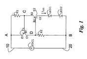
- the linear current regulation device according to the diagram of Figure 1 is an example of a solution presently used for the purpose.
- the device comprises two bipolar transistors (BJT), in this case of a pnp type, indicated by the reference numbers T1 and T2, and two resistances R1 and R2.
- BJT bipolar transistors
- the positive terminal of a direct voltage input generator VDC1 is connected to the emitter E1 of the first transistor T1 (node A).
- the resistance R1 is connected between the emitter E1 and the base B1 of the first transistor T1.
- the emitter E2 of the second transistor T2 is connected (node C) to the base B1.
- the collector C1 of the first transistor T1 is connected, via the node D, to the base B2 of the second transistor T2.
- the resistance R2 is connected between the node D and the node B, i.e. the negative terminal of the voltage generator VDC1.
- the collector C2 of the second transistor T2 feeds the series of both LED1 and LED2.
- the cathode of the second diode LED2 is connected to the above mentioned node B on the second supply line 20.
- the high-impedance resistance R2 polarizes the first transistor T1 with a very low collector current Ic ( ⁇ A), but the base-emitter voltage V BE1 of the first transistor T1 is set to the value V BEon .
- the transistor T2 is therefore used as a driver circuit of the LEDs, while the transistor T1 has a stabilizing function.
- the collector current I C2 of the driver transistor T2 drives the light sources LED1 and LED 2 and the stabilization circuit T1, R1, R2 generates a reference voltage V BE1 - stable with reference to the input voltage VDC1 - which, applied to the transistor T2, makes the current I LED flowing through the LEDs equally stable with reference to the input voltage VDC1. The consequence is a stabilization of the current I LED with reference to the input voltage VDC1.
- a possible range of the operating temperatures of LED modules goes from -30°C to +80°C, because of the different ambient conditions where they can be employed.
- the base-emitter junction voltage of the transistor T1 varies with the temperature T on the basis of a coefficient k (mV/°C).
- I LED T V BE ⁇ 1 T
- R 1 V BE ⁇ 1 T ⁇ 0 + k ⁇ ⁇ T
- R 1 V BE ⁇ 1 T ⁇ 0 + k ⁇ T - T ⁇ 0
- R 1 V BE ⁇ 1 T ⁇ 0
- the value of the current I LED (T) at a given temperature T is therefore given by the value of the current I LED (T0) flowing in the LEDs at the reference temperature of 25°C with a variation ⁇ I LED (T) (positive or negative) which depends on the temperature T.
- a typical value for the coefficient k for a p-n junction is -2 mV/°C.
- the LED module input power could have a variation of ⁇ 20% from the rated input power at a reference ambient temperature of 25°C.
- a driver device for a LED lighting system wherein two transistors are connected to a LED load in order to stabilize and to maintain the LED current in a safe operating area in relationship with temperature variations. Such an arrangement does not allow to keep the load current constant when temperature variation occurs.
- drivers for light sources for example LEDs (Light Emitting Diodes), capable of performing a linear regulation of the current, while allowing to obtain a thermal stabilization of the current itself.
- LEDs Light Emitting Diodes
- the object of the invention is to provide such a device.
- a linear current regulation driver is achieved using three bipolar transistors (BJT), respectively indicated with the references T1a, T1b and T2, here of the npn type, and five resistances (resistors) R1, R2, R3, R4 and RS.
- BJT bipolar transistors
- At least the transistor T2 can be a field effect transistor, such as a MOSFET.
- a field effect transistor such as a MOSFET.
- the circuit is supposed to drive a load made up of a light source, comprising two diodes LED connected in series, indicated with LED1 and LED2.
- a first input line 30 is connected, comprising the resistances R1 and R2, that serve primarily as polarization resistances of the transistors T1a and T1b, particularly (as will be detailed in the following) as regards the setting of the values of the respective base-emitter voltages.
- the resistance R1 is interposed between the supply line 30 (node L) and the collector C1b of the transistor T1b, while the resistance R2 is interposed between the supply line 30 (node M) and the collector C1a of the transistor T1a.
- the transistor T1b has the base B1b and the collector C1b mutually connected (node O, that coincides with node P), so as to function essentially as a diode.
- the resistances R3 and R4 form a voltage divider between the base B1b of the transistor T1b and the base B1a of the transistor T1a.
- the resistance R3 is interposed (as a "high” branch of the divider) between the bases B1a and B1b of the two transistors T1a and T1b, while the resistance R4 is interposed (as a "low” branch of the divider) between a node Q, arranged between the base B1a of the transistor T1a and the resistance R3, and a second supply line 40 leading to the negative terminal of the voltage generator VDC1 (node S).
- the emitter E1a of the transistor T1a is connected to the second line 40 as well, via the node V.
- the resistance R2 is connected between the first supply line 30 (node M) and the node N, to which in turn the collector C1a of the transistor T1a and the base B2 of the transistor T2 are connected.
- the emitter E1b of the transistor T1b and the emitter E2 are mutually connected in a node R, to which also the resistance RS is connected, obtaining a function of amperometric resistor sensing the current flowing through the load, i.e. through the diodes LED1 and LED2 (for example to perform regulation functions that are not specifically considered herein).
- the resistance RS is connected between said node S and node R.
- the two diodes LED1 and LED2 are connected in a series configuration and the anode of LED1 is connected to node M, while the cathode of LED2 is connected to collector C2 of the transistor T2; therefore, through the two LEDs a current flows that equals the collector current of the transistor T2.
- the function of thermal stabilization makes use of the fact that the base-emitter voltage drop V BE of a bipolar transistor varies with the temperature T during use.
- the value of the resistance R1 is chosen as to supply the transistor T1b with such a current as to establish, between base and emitter, a voltage V BE1bON , which is the stable reference voltage of the circuit applied to the driver transistor T2.
- the current flowing through Rs is determined by the mesh stabilization given by R3, R4, T 1bon and Rs.
- the voltage T 1bon added to the voltage VRs, through the voltage divider made up by R3 and R4, must correspond to the voltage T 1aon (which is the same as VR4).
- the voltage VRs stabilizes and, on the basis of the value of Rs, it is possible to set the needed current I LED .
- the electrical and thermal behaviour of the circuit can be improved making use of the fact that bipolar transistors such as the transistors T1a and T1b have the same thermal behaviour, particularly as regards their base-emitter junction, so that their thermal drifts are compensated.
- this result is achieved by choosing the transistors T1a and T1b mutually identical.
- T1a and T1b are on the same integrated component (and so both transistors are subjected to the same temperature).
- T1a and T1b are a pair of integrated monolithic components.
- V BE1bON is set and I LED is fixed, the values of R3, R4 (and RS) may be chosen so as to minimize the current variation due to the thermal behaviour of the p-n junctions of T1a and T1b.
- ⁇ ⁇ I LED ⁇ ⁇ V BE ⁇ 1 ⁇ aON R S ⁇ R 3 + R 4 R 4 - ⁇ ⁇ V BE ⁇ 1 ⁇ bON R S
- I LED T I LED T ⁇ 0 1 + k ⁇ R 3 ⁇ T - T 0 V BE ⁇ 1 ⁇ aON ⁇ R 3 + R 4 - V BE ⁇ 1 ⁇ bON ⁇ R 4
- V BE1aON , V BE1bON , R3 and R4 the denominator V BE 1 aON ⁇ ( R 3 + R 4 ) -V BE 1 bON ⁇ R 4 modifies the value of H2 in different ways.
- V BE1aON >V BE1bON represents the best solution in order to control the current variation I LED with reference to the temperature variation T, and it is obtained only modifying the values of the resistances R3 and R4.
- a current variation I LED (-30°C) has been detected at a temperature of -30 °C, as compared to the current I LED (25 °C) at ambient temperature in the case V BE1aON is 0,65 V, R4 is 10k ⁇ and V BE1bON is 0,62 V.
- Table 1 that follows summarizes, as a function of different values of the quantities considered in the foregoing, the data of current variation I LED as a function of temperature T.
- Table 1 Values of the components R1 10k 30k 30k 30k 47k R2 10k 10k 10k 10k 10k R3 1k 1k 4.7k 0.56k 1k R4 10k 10k 4.7k 10k 10k Ratio 0.907063197 0.907063197 0.5 0.996969697 0.907063197 V BE1aON 0.597 0.629 0.622 0.628 0.622 V BE1bON 0.597 0.599 0.591 0.588 0.577 ⁇ V BEON 0 0.03 0.031 0.04 0.045 RS 2.2 3.9 18 1.8 3.2 Standard T(°C) I LED A I LED B I LED C I LED D I LED E sol.
- the upper part of the Table shows the values of the components and the corresponding value of the ratio corresponding to (R4/(R3+R4)).
- the central and the lower parts of the Table show on the contrary the different current values through the LEDs for different temperatures, such values being shown both in their absolute value and as a percentage of the value at 25°C.
- "standard sol.” indicated the standard solution discussed in the introductory part of the description, with reference to Figure 1 .
- the value of the sensing resistance RS does not in itself take on a decisive role in achieving the results, even though such a resistance determines a voltage drop between the points R and S (and therefore V) that makes it possible to fulfil the condition V BE1aON > V BE1bON .
- the details and the embodiments may vary, even appreciably, with respect to what has been described by way of example only, without departing from the scope of the invention as defined by the annexed claims.
- the presently described solution can be carried out in an embodiment in which at least the driver transistor T2 is a MOSFET and/or it can be used in general to obtain a current regulator with low drop-out for applications other than light source driving.
Landscapes
- Led Devices (AREA)
- Continuous-Control Power Sources That Use Transistors (AREA)
Claims (10)
- Eine Treibervorrichtung, um einen geregelten Strom (ILED) aus einer Eingangsspannung (VDC1) zu erzeugen, umfassend:- einen Treibertransistor (T2) zum Bereitstellen des geregelten Stroms (ILED), und- einen Stabilisationsschaltkreis (T1a, T1b, R1, R2, R3, R4, RS) zum Erzeugen, von der Eingangsspannung (VDC1), einer stabilisierten Referenzspannung (VBE1bON), zum Anlegen an den Treibertransistor (T2), wobei der Stabilisationsschaltkreis umfasst:- einen ersten (T1a) und einen zweiten (T1b) bipolaren Stabilisationstransistor, wobei die Basis-Emitter Spannung (VBE1bON) des zweiten Stabilisationstransistors (T1b) die stabilisierte Referenzspannung (VBE1bON) für den Treibertransistor (T2) bestimmt;- einen Spannungsteiler (R3, R4), der einen ersten (R3) und einen zweiten (R4) Widerstand umfasst, wobei der Spannungsteiler (R3, R4) zwischen den Basen des ersten (T1a) und des zweiten (T1b) Stabilisationstransistors geschaltet ist, wobei der erste Widerstand (R3) zwischen der Basis des zweiten Stabilisationstransistors (T1b) und dem Teilungspunkt (Q) des Spannungsteilers verbunden ist, und der Teilpunkt (Q) als die Basis des ersten Stabilisationstransistors (T1a) wirkt; und- ein Polarisationsnetzwerk (R1, R2, RS) um die Basis-Emitter Spannungen (VBE1aON, VBE1bON), des ersten (T1a) und des zweiten (T1b) Stabilisationstransistors zu bestimmen, wobei das Polarisationsnetzwerk einen Widerstand (RS) umfasst, der zwischen den Emittern des ersten (T1a) und des zweiten (T1b) Stabilisationstransistors wirkt, um einen Spannungsabfall zwischen den Emittern herbeizuführen, und:- i) der zweite Stabilisationstransistor (T1b) ist diodenverbunden mit dem Kollektor, der mit der Basis verbunden ist,- ii) der erste Widerstand (R3) des Spannungsteilers hat einen Wert, der niedriger ist, als der Wert des zweiten Widerstands (R4) des Spannungsteilers, und- iii) die Basis-Emitter Spannung (VBE1aON) des ersten Stabilisationstransistors (T1a) is höher, als die Basis-Emitter Spannung (VBE1bON) des zweiten Stabilisationstransistors (T1b).
- Vorrichtung nach Anspruch 1, wobei der erste Widerstand (R3) des Spannungsteilers einen Wert von ungefähr gleich 1/10 des Wertes des zweiten Widerstandes (R4) des Spannungsteilers aufweist.
- Vorrichtung nach Anspruch 1, wobei der erste Widerstand (R3) des Spannungsteilers einen Wert aufweist, der niedriger ist, als 1/10 des Wertes des zweiten Widerstandes (R4) des Spannungsteilers.
- Vorrichtung nach irgendeinem der vorhergehenden Ansprüche, wobei das Polarisationsnetzwerk entsprechende Widerstände (R1, R2) umfasst, die zwischen der Eingangsspannung (VDC1) und den Kollektoren des ersten (T1a) und des zweiten (T1b) Stabilisationstransistors wirken.
- Treiberschaltung nach irgendeinem der vorhergehenden Ansprüche, wobei der erste (T1a) und zweite (T1b) Stabilisationstransistor identisch zueinander sind.
- Treiberschaltung nach irgendeinem der vorhergehenden Ansprüche, wobei der erste (T1a) und der zweite (T1b) Stabilisationstransistor auf einer gemeinsamen Unterlage montiert sind, um der selben Temperatur unterworfen zu sein.
- Vorrichtung nach irgendeinem der vorhergehenden Ansprüche, wobei der erste (T1a) und der zweite (T1b) Stabilisationstransistor ein Paar an monolithischen integrierten Komponenten bilden.
- Vorrichtung nach irgendeinem der vorhergehenden Ansprüche, wobei der Treibertransistor (T2) ein Bipolartransistor ist.
- Vorrichtung nach irgendeinem der vorhergehenden Ansprüche 1 bis 8, wobei der Treibertransistor (T2) ein MOSFET Transistor ist.
- Vorrichtung nach irgendeinem der vorhergehenden Ansprüche, wobei der Treibertransistor (T2) mit einer Lichtquelle gekoppelt ist, wie einer LED Lichtquelle (LED1, LED2), die von dem geregelten Strom (ILED) getrieben wird.
Applications Claiming Priority (1)
| Application Number | Priority Date | Filing Date | Title |
|---|---|---|---|
| ITTO20090358 | 2009-05-04 |
Publications (3)
| Publication Number | Publication Date |
|---|---|
| EP2249622A1 EP2249622A1 (de) | 2010-11-10 |
| EP2249622A8 EP2249622A8 (de) | 2011-02-09 |
| EP2249622B1 true EP2249622B1 (de) | 2011-09-07 |
Family
ID=42617532
Family Applications (1)
| Application Number | Title | Priority Date | Filing Date |
|---|---|---|---|
| EP10161521A Not-in-force EP2249622B1 (de) | 2009-05-04 | 2010-04-29 | Temperaturstabilisierter Stromregeltreiber |
Country Status (5)
| Country | Link |
|---|---|
| US (1) | US8633652B2 (de) |
| EP (1) | EP2249622B1 (de) |
| KR (1) | KR101065528B1 (de) |
| CN (1) | CN101883459A (de) |
| AT (1) | ATE524050T1 (de) |
Families Citing this family (4)
| Publication number | Priority date | Publication date | Assignee | Title |
|---|---|---|---|---|
| DE102010028795A1 (de) * | 2010-05-10 | 2011-11-10 | Osram Gesellschaft mit beschränkter Haftung | Schaltung zum Betrieb einer Leuchteinheit sowie Leuchte mit einer solchen Schaltung |
| ITCS20110016A1 (it) * | 2011-06-17 | 2012-12-18 | E D P Srl | Sistema elettronico di alimentazione e regolazione della corrente per lampade a led |
| GB2492551A (en) | 2011-07-04 | 2013-01-09 | Accuric Ltd | Current regulator |
| EP3474632B1 (de) * | 2017-10-19 | 2020-07-15 | ZKW Group GmbH | Schaltungsanordnung zum erzeugen einer referenzspannung für die stromversorgung einer led-anordnung |
Family Cites Families (9)
| Publication number | Priority date | Publication date | Assignee | Title |
|---|---|---|---|---|
| US5701133A (en) * | 1994-10-13 | 1997-12-23 | Lucent Technologies Inc. | Cascaded multiplying current mirror driver for LED's |
| JP2004039290A (ja) | 2002-06-28 | 2004-02-05 | Matsushita Electric Works Ltd | 照明装置 |
| JP2005057094A (ja) * | 2003-08-05 | 2005-03-03 | Agilent Technologies Japan Ltd | 発光ダイオードの駆動回路 |
| US7064529B2 (en) | 2003-09-17 | 2006-06-20 | Atmel Corporation | Dual stage voltage regulation circuit |
| US7211967B2 (en) * | 2003-11-21 | 2007-05-01 | Yuan Lin | Strip light with constant current |
| TWI242323B (en) * | 2004-02-12 | 2005-10-21 | Airoha Tech Corp | Gain control circuit and gain amplifier using the same |
| FR2872645B1 (fr) | 2004-07-02 | 2006-09-22 | Atmel Corp | Dispositif de conversion de puissance avec detecteur efficace de courant de sortie |
| US7847486B2 (en) * | 2004-08-04 | 2010-12-07 | Dr. LED (Holdings), Inc | LED lighting system |
| CN101032188A (zh) | 2004-08-04 | 2007-09-05 | 詹姆斯·K·吴 | Led照明系统 |
-
2010
- 2010-04-29 EP EP10161521A patent/EP2249622B1/de not_active Not-in-force
- 2010-04-29 AT AT10161521T patent/ATE524050T1/de not_active IP Right Cessation
- 2010-04-30 US US12/770,933 patent/US8633652B2/en not_active Expired - Fee Related
- 2010-05-03 KR KR1020100041389A patent/KR101065528B1/ko not_active Expired - Fee Related
- 2010-05-04 CN CN2010101702446A patent/CN101883459A/zh active Pending
Also Published As
| Publication number | Publication date |
|---|---|
| KR101065528B1 (ko) | 2011-09-19 |
| US8633652B2 (en) | 2014-01-21 |
| EP2249622A1 (de) | 2010-11-10 |
| KR20100120087A (ko) | 2010-11-12 |
| CN101883459A (zh) | 2010-11-10 |
| EP2249622A8 (de) | 2011-02-09 |
| ATE524050T1 (de) | 2011-09-15 |
| US20100277091A1 (en) | 2010-11-04 |
Similar Documents
| Publication | Publication Date | Title |
|---|---|---|
| US7683553B2 (en) | LED current control circuits and methods | |
| US8941325B2 (en) | Light emitting device array driver circuit and current splitter circuit and method of splitting current therefor | |
| US9491824B2 (en) | Method and apparatus for precise temperature brightness compensation of LED | |
| US7839097B2 (en) | System and method for wide-range high-accuracy-low-dropout current regulation | |
| EP1980140A1 (de) | Temperaturgesteuerte led-ausrichtung | |
| JPH04137116A (ja) | 電流制御装置 | |
| EP2249622B1 (de) | Temperaturstabilisierter Stromregeltreiber | |
| EP2584871A1 (de) | Antriebsvorrichtung für ein organisches el-element und organische el-beleuchtungsvorrichtung | |
| KR101935626B1 (ko) | 전류조정기 | |
| EP2249623A1 (de) | Ein Stromregler mit geringen Abfallstrom | |
| CN109309986B (zh) | 一种自恒流保护电路及恒流驱动电路 | |
| JP2012064009A (ja) | 電圧出力回路 | |
| US9961729B1 (en) | Trimming system and method for regulated current mirrors | |
| US20070200546A1 (en) | Reference voltage generating circuit for generating low reference voltages | |
| JP2011258616A (ja) | Led駆動回路 | |
| KR100979835B1 (ko) | 발광 다이오드 조명을 위한 정전류 공급 장치 | |
| US6356066B1 (en) | Voltage reference source | |
| CN121725726A (zh) | Led驱动电路及显示系统 | |
| EP3772822A1 (de) | Konstantstromtreibervorrichtung | |
| JPH02132874A (ja) | 温度安定化レーザダイオードモジュール | |
| NZ620582B2 (en) | Current regulator |
Legal Events
| Date | Code | Title | Description |
|---|---|---|---|
| PUAI | Public reference made under article 153(3) epc to a published international application that has entered the european phase |
Free format text: ORIGINAL CODE: 0009012 |
|
| AK | Designated contracting states |
Kind code of ref document: A1 Designated state(s): AT BE BG CH CY CZ DE DK EE ES FI FR GB GR HR HU IE IS IT LI LT LU LV MC MK MT NL NO PL PT RO SE SI SK SM TR |
|
| AX | Request for extension of the european patent |
Extension state: AL BA ME RS |
|
| RAP1 | Party data changed (applicant data changed or rights of an application transferred) |
Owner name: OSRAM GESELLSCHAFT MIT BESCHRAENKTER HAFTUNG Owner name: OSRAM S.P.A. - SOCIETA' RIUNITE OSRAM EDISON CLERI |
|
| 17P | Request for examination filed |
Effective date: 20110214 |
|
| GRAP | Despatch of communication of intention to grant a patent |
Free format text: ORIGINAL CODE: EPIDOSNIGR1 |
|
| RIC1 | Information provided on ipc code assigned before grant |
Ipc: H05B 33/08 20060101AFI20110309BHEP |
|
| RIN1 | Information on inventor provided before grant (corrected) |
Inventor name: TOSCAN, MATTEO Inventor name: BRIEDA, ALESSANDRO |
|
| GRAS | Grant fee paid |
Free format text: ORIGINAL CODE: EPIDOSNIGR3 |
|
| GRAA | (expected) grant |
Free format text: ORIGINAL CODE: 0009210 |
|
| REG | Reference to a national code |
Ref country code: GB Ref legal event code: FG4D |
|
| REG | Reference to a national code |
Ref country code: CH Ref legal event code: EP |
|
| RAP2 | Party data changed (patent owner data changed or rights of a patent transferred) |
Owner name: OSRAM AG Owner name: OSRAM S.P.A. - SOCIETA' RIUNITE OSRAM EDISON CLERI |
|
| REG | Reference to a national code |
Ref country code: IE Ref legal event code: FG4D |
|
| REG | Reference to a national code |
Ref country code: DE Ref legal event code: R096 Ref document number: 602010000179 Country of ref document: DE Effective date: 20111110 |
|
| REG | Reference to a national code |
Ref country code: NL Ref legal event code: VDEP Effective date: 20110907 |
|
| PG25 | Lapsed in a contracting state [announced via postgrant information from national office to epo] |
Ref country code: HR Free format text: LAPSE BECAUSE OF FAILURE TO SUBMIT A TRANSLATION OF THE DESCRIPTION OR TO PAY THE FEE WITHIN THE PRESCRIBED TIME-LIMIT Effective date: 20110907 Ref country code: SE Free format text: LAPSE BECAUSE OF FAILURE TO SUBMIT A TRANSLATION OF THE DESCRIPTION OR TO PAY THE FEE WITHIN THE PRESCRIBED TIME-LIMIT Effective date: 20110907 Ref country code: NO Free format text: LAPSE BECAUSE OF FAILURE TO SUBMIT A TRANSLATION OF THE DESCRIPTION OR TO PAY THE FEE WITHIN THE PRESCRIBED TIME-LIMIT Effective date: 20111207 Ref country code: LT Free format text: LAPSE BECAUSE OF FAILURE TO SUBMIT A TRANSLATION OF THE DESCRIPTION OR TO PAY THE FEE WITHIN THE PRESCRIBED TIME-LIMIT Effective date: 20110907 Ref country code: FI Free format text: LAPSE BECAUSE OF FAILURE TO SUBMIT A TRANSLATION OF THE DESCRIPTION OR TO PAY THE FEE WITHIN THE PRESCRIBED TIME-LIMIT Effective date: 20110907 |
|
| LTIE | Lt: invalidation of european patent or patent extension |
Effective date: 20110907 |
|
| PG25 | Lapsed in a contracting state [announced via postgrant information from national office to epo] |
Ref country code: LV Free format text: LAPSE BECAUSE OF FAILURE TO SUBMIT A TRANSLATION OF THE DESCRIPTION OR TO PAY THE FEE WITHIN THE PRESCRIBED TIME-LIMIT Effective date: 20110907 Ref country code: GR Free format text: LAPSE BECAUSE OF FAILURE TO SUBMIT A TRANSLATION OF THE DESCRIPTION OR TO PAY THE FEE WITHIN THE PRESCRIBED TIME-LIMIT Effective date: 20111208 Ref country code: CY Free format text: LAPSE BECAUSE OF FAILURE TO SUBMIT A TRANSLATION OF THE DESCRIPTION OR TO PAY THE FEE WITHIN THE PRESCRIBED TIME-LIMIT Effective date: 20110907 Ref country code: AT Free format text: LAPSE BECAUSE OF FAILURE TO SUBMIT A TRANSLATION OF THE DESCRIPTION OR TO PAY THE FEE WITHIN THE PRESCRIBED TIME-LIMIT Effective date: 20110907 Ref country code: SI Free format text: LAPSE BECAUSE OF FAILURE TO SUBMIT A TRANSLATION OF THE DESCRIPTION OR TO PAY THE FEE WITHIN THE PRESCRIBED TIME-LIMIT Effective date: 20110907 |
|
| REG | Reference to a national code |
Ref country code: AT Ref legal event code: MK05 Ref document number: 524050 Country of ref document: AT Kind code of ref document: T Effective date: 20110907 |
|
| PG25 | Lapsed in a contracting state [announced via postgrant information from national office to epo] |
Ref country code: BE Free format text: LAPSE BECAUSE OF FAILURE TO SUBMIT A TRANSLATION OF THE DESCRIPTION OR TO PAY THE FEE WITHIN THE PRESCRIBED TIME-LIMIT Effective date: 20110907 |
|
| PG25 | Lapsed in a contracting state [announced via postgrant information from national office to epo] |
Ref country code: IS Free format text: LAPSE BECAUSE OF FAILURE TO SUBMIT A TRANSLATION OF THE DESCRIPTION OR TO PAY THE FEE WITHIN THE PRESCRIBED TIME-LIMIT Effective date: 20120107 Ref country code: CZ Free format text: LAPSE BECAUSE OF FAILURE TO SUBMIT A TRANSLATION OF THE DESCRIPTION OR TO PAY THE FEE WITHIN THE PRESCRIBED TIME-LIMIT Effective date: 20110907 Ref country code: SK Free format text: LAPSE BECAUSE OF FAILURE TO SUBMIT A TRANSLATION OF THE DESCRIPTION OR TO PAY THE FEE WITHIN THE PRESCRIBED TIME-LIMIT Effective date: 20110907 |
|
| PG25 | Lapsed in a contracting state [announced via postgrant information from national office to epo] |
Ref country code: EE Free format text: LAPSE BECAUSE OF FAILURE TO SUBMIT A TRANSLATION OF THE DESCRIPTION OR TO PAY THE FEE WITHIN THE PRESCRIBED TIME-LIMIT Effective date: 20110907 Ref country code: NL Free format text: LAPSE BECAUSE OF FAILURE TO SUBMIT A TRANSLATION OF THE DESCRIPTION OR TO PAY THE FEE WITHIN THE PRESCRIBED TIME-LIMIT Effective date: 20110907 Ref country code: RO Free format text: LAPSE BECAUSE OF FAILURE TO SUBMIT A TRANSLATION OF THE DESCRIPTION OR TO PAY THE FEE WITHIN THE PRESCRIBED TIME-LIMIT Effective date: 20110907 Ref country code: PL Free format text: LAPSE BECAUSE OF FAILURE TO SUBMIT A TRANSLATION OF THE DESCRIPTION OR TO PAY THE FEE WITHIN THE PRESCRIBED TIME-LIMIT Effective date: 20110907 Ref country code: PT Free format text: LAPSE BECAUSE OF FAILURE TO SUBMIT A TRANSLATION OF THE DESCRIPTION OR TO PAY THE FEE WITHIN THE PRESCRIBED TIME-LIMIT Effective date: 20120109 Ref country code: IT Free format text: LAPSE BECAUSE OF FAILURE TO SUBMIT A TRANSLATION OF THE DESCRIPTION OR TO PAY THE FEE WITHIN THE PRESCRIBED TIME-LIMIT Effective date: 20110907 |
|
| REG | Reference to a national code |
Ref country code: DE Ref legal event code: R084 Ref document number: 602010000179 Country of ref document: DE Effective date: 20120423 |
|
| PLBE | No opposition filed within time limit |
Free format text: ORIGINAL CODE: 0009261 |
|
| STAA | Information on the status of an ep patent application or granted ep patent |
Free format text: STATUS: NO OPPOSITION FILED WITHIN TIME LIMIT |
|
| PG25 | Lapsed in a contracting state [announced via postgrant information from national office to epo] |
Ref country code: DK Free format text: LAPSE BECAUSE OF FAILURE TO SUBMIT A TRANSLATION OF THE DESCRIPTION OR TO PAY THE FEE WITHIN THE PRESCRIBED TIME-LIMIT Effective date: 20110907 |
|
| 26N | No opposition filed |
Effective date: 20120611 |
|
| REG | Reference to a national code |
Ref country code: DE Ref legal event code: R097 Ref document number: 602010000179 Country of ref document: DE Effective date: 20120611 |
|
| PG25 | Lapsed in a contracting state [announced via postgrant information from national office to epo] |
Ref country code: MC Free format text: LAPSE BECAUSE OF NON-PAYMENT OF DUE FEES Effective date: 20120430 |
|
| PG25 | Lapsed in a contracting state [announced via postgrant information from national office to epo] |
Ref country code: MK Free format text: LAPSE BECAUSE OF FAILURE TO SUBMIT A TRANSLATION OF THE DESCRIPTION OR TO PAY THE FEE WITHIN THE PRESCRIBED TIME-LIMIT Effective date: 20110907 |
|
| REG | Reference to a national code |
Ref country code: DE Ref legal event code: R081 Ref document number: 602010000179 Country of ref document: DE Owner name: OSRAM GMBH, DE Free format text: FORMER OWNER: OSRAM AG, 81543 MUENCHEN, DE Effective date: 20130205 |
|
| PG25 | Lapsed in a contracting state [announced via postgrant information from national office to epo] |
Ref country code: ES Free format text: LAPSE BECAUSE OF FAILURE TO SUBMIT A TRANSLATION OF THE DESCRIPTION OR TO PAY THE FEE WITHIN THE PRESCRIBED TIME-LIMIT Effective date: 20111218 Ref country code: IE Free format text: LAPSE BECAUSE OF NON-PAYMENT OF DUE FEES Effective date: 20120429 |
|
| PG25 | Lapsed in a contracting state [announced via postgrant information from national office to epo] |
Ref country code: BG Free format text: LAPSE BECAUSE OF FAILURE TO SUBMIT A TRANSLATION OF THE DESCRIPTION OR TO PAY THE FEE WITHIN THE PRESCRIBED TIME-LIMIT Effective date: 20111207 |
|
| PG25 | Lapsed in a contracting state [announced via postgrant information from national office to epo] |
Ref country code: MT Free format text: LAPSE BECAUSE OF FAILURE TO SUBMIT A TRANSLATION OF THE DESCRIPTION OR TO PAY THE FEE WITHIN THE PRESCRIBED TIME-LIMIT Effective date: 20110907 |
|
| PGFP | Annual fee paid to national office [announced via postgrant information from national office to epo] |
Ref country code: FR Payment date: 20130515 Year of fee payment: 4 |
|
| REG | Reference to a national code |
Ref country code: DE Ref legal event code: R081 Ref document number: 602010000179 Country of ref document: DE Owner name: OSRAM GMBH, DE Free format text: FORMER OWNER: OSRAM GMBH, 81543 MUENCHEN, DE Effective date: 20130829 |
|
| PG25 | Lapsed in a contracting state [announced via postgrant information from national office to epo] |
Ref country code: TR Free format text: LAPSE BECAUSE OF FAILURE TO SUBMIT A TRANSLATION OF THE DESCRIPTION OR TO PAY THE FEE WITHIN THE PRESCRIBED TIME-LIMIT Effective date: 20110907 |
|
| PG25 | Lapsed in a contracting state [announced via postgrant information from national office to epo] |
Ref country code: SM Free format text: LAPSE BECAUSE OF FAILURE TO SUBMIT A TRANSLATION OF THE DESCRIPTION OR TO PAY THE FEE WITHIN THE PRESCRIBED TIME-LIMIT Effective date: 20110907 Ref country code: LU Free format text: LAPSE BECAUSE OF NON-PAYMENT OF DUE FEES Effective date: 20120429 |
|
| PG25 | Lapsed in a contracting state [announced via postgrant information from national office to epo] |
Ref country code: HU Free format text: LAPSE BECAUSE OF FAILURE TO SUBMIT A TRANSLATION OF THE DESCRIPTION OR TO PAY THE FEE WITHIN THE PRESCRIBED TIME-LIMIT Effective date: 20100429 |
|
| REG | Reference to a national code |
Ref country code: CH Ref legal event code: PL |
|
| GBPC | Gb: european patent ceased through non-payment of renewal fee |
Effective date: 20140429 |
|
| REG | Reference to a national code |
Ref country code: FR Ref legal event code: ST Effective date: 20141231 |
|
| PG25 | Lapsed in a contracting state [announced via postgrant information from national office to epo] |
Ref country code: CH Free format text: LAPSE BECAUSE OF NON-PAYMENT OF DUE FEES Effective date: 20140430 Ref country code: GB Free format text: LAPSE BECAUSE OF NON-PAYMENT OF DUE FEES Effective date: 20140429 Ref country code: LI Free format text: LAPSE BECAUSE OF NON-PAYMENT OF DUE FEES Effective date: 20140430 |
|
| PG25 | Lapsed in a contracting state [announced via postgrant information from national office to epo] |
Ref country code: FR Free format text: LAPSE BECAUSE OF NON-PAYMENT OF DUE FEES Effective date: 20140430 |
|
| PGFP | Annual fee paid to national office [announced via postgrant information from national office to epo] |
Ref country code: DE Payment date: 20190418 Year of fee payment: 10 |
|
| REG | Reference to a national code |
Ref country code: DE Ref legal event code: R079 Ref document number: 602010000179 Country of ref document: DE Free format text: PREVIOUS MAIN CLASS: H05B0033080000 Ipc: H05B0045000000 |
|
| REG | Reference to a national code |
Ref country code: DE Ref legal event code: R119 Ref document number: 602010000179 Country of ref document: DE |
|
| PG25 | Lapsed in a contracting state [announced via postgrant information from national office to epo] |
Ref country code: DE Free format text: LAPSE BECAUSE OF NON-PAYMENT OF DUE FEES Effective date: 20201103 |