EP2251464A2 - Epitaxiesubstrat für Halbleiterbauelement, Halbleiterbauelement und Verfahren zur Herstellung eines Epitaxiesubstrats für ein Halbleiterbauelement - Google Patents
Epitaxiesubstrat für Halbleiterbauelement, Halbleiterbauelement und Verfahren zur Herstellung eines Epitaxiesubstrats für ein Halbleiterbauelement Download PDFInfo
- Publication number
- EP2251464A2 EP2251464A2 EP10250839A EP10250839A EP2251464A2 EP 2251464 A2 EP2251464 A2 EP 2251464A2 EP 10250839 A EP10250839 A EP 10250839A EP 10250839 A EP10250839 A EP 10250839A EP 2251464 A2 EP2251464 A2 EP 2251464A2
- Authority
- EP
- European Patent Office
- Prior art keywords
- layer
- semiconductor device
- barrier layer
- epitaxial substrate
- composition
- Prior art date
- Legal status (The legal status is an assumption and is not a legal conclusion. Google has not performed a legal analysis and makes no representation as to the accuracy of the status listed.)
- Granted
Links
Images







Classifications
-
- C—CHEMISTRY; METALLURGY
- C30—CRYSTAL GROWTH
- C30B—SINGLE-CRYSTAL GROWTH; UNIDIRECTIONAL SOLIDIFICATION OF EUTECTIC MATERIAL OR UNIDIRECTIONAL DEMIXING OF EUTECTOID MATERIAL; REFINING BY ZONE-MELTING OF MATERIAL; PRODUCTION OF A HOMOGENEOUS POLYCRYSTALLINE MATERIAL WITH DEFINED STRUCTURE; SINGLE CRYSTALS OR HOMOGENEOUS POLYCRYSTALLINE MATERIAL WITH DEFINED STRUCTURE; AFTER-TREATMENT OF SINGLE CRYSTALS OR A HOMOGENEOUS POLYCRYSTALLINE MATERIAL WITH DEFINED STRUCTURE; APPARATUS THEREFOR
- C30B25/00—Single-crystal growth by chemical reaction of reactive gases, e.g. chemical vapour-deposition growth
- C30B25/02—Epitaxial-layer growth
-
- C—CHEMISTRY; METALLURGY
- C30—CRYSTAL GROWTH
- C30B—SINGLE-CRYSTAL GROWTH; UNIDIRECTIONAL SOLIDIFICATION OF EUTECTIC MATERIAL OR UNIDIRECTIONAL DEMIXING OF EUTECTOID MATERIAL; REFINING BY ZONE-MELTING OF MATERIAL; PRODUCTION OF A HOMOGENEOUS POLYCRYSTALLINE MATERIAL WITH DEFINED STRUCTURE; SINGLE CRYSTALS OR HOMOGENEOUS POLYCRYSTALLINE MATERIAL WITH DEFINED STRUCTURE; AFTER-TREATMENT OF SINGLE CRYSTALS OR A HOMOGENEOUS POLYCRYSTALLINE MATERIAL WITH DEFINED STRUCTURE; APPARATUS THEREFOR
- C30B19/00—Liquid-phase epitaxial-layer growth
-
- C—CHEMISTRY; METALLURGY
- C30—CRYSTAL GROWTH
- C30B—SINGLE-CRYSTAL GROWTH; UNIDIRECTIONAL SOLIDIFICATION OF EUTECTIC MATERIAL OR UNIDIRECTIONAL DEMIXING OF EUTECTOID MATERIAL; REFINING BY ZONE-MELTING OF MATERIAL; PRODUCTION OF A HOMOGENEOUS POLYCRYSTALLINE MATERIAL WITH DEFINED STRUCTURE; SINGLE CRYSTALS OR HOMOGENEOUS POLYCRYSTALLINE MATERIAL WITH DEFINED STRUCTURE; AFTER-TREATMENT OF SINGLE CRYSTALS OR A HOMOGENEOUS POLYCRYSTALLINE MATERIAL WITH DEFINED STRUCTURE; APPARATUS THEREFOR
- C30B23/00—Single-crystal growth by condensing evaporated or sublimed materials
- C30B23/02—Epitaxial-layer growth
-
- C—CHEMISTRY; METALLURGY
- C30—CRYSTAL GROWTH
- C30B—SINGLE-CRYSTAL GROWTH; UNIDIRECTIONAL SOLIDIFICATION OF EUTECTIC MATERIAL OR UNIDIRECTIONAL DEMIXING OF EUTECTOID MATERIAL; REFINING BY ZONE-MELTING OF MATERIAL; PRODUCTION OF A HOMOGENEOUS POLYCRYSTALLINE MATERIAL WITH DEFINED STRUCTURE; SINGLE CRYSTALS OR HOMOGENEOUS POLYCRYSTALLINE MATERIAL WITH DEFINED STRUCTURE; AFTER-TREATMENT OF SINGLE CRYSTALS OR A HOMOGENEOUS POLYCRYSTALLINE MATERIAL WITH DEFINED STRUCTURE; APPARATUS THEREFOR
- C30B29/00—Single crystals or homogeneous polycrystalline material with defined structure characterised by the material or by their shape
- C30B29/10—Inorganic compounds or compositions
- C30B29/40—AIIIBV compounds wherein A is B, Al, Ga, In or Tl and B is N, P, As, Sb or Bi
- C30B29/403—AIII-nitrides
-
- C—CHEMISTRY; METALLURGY
- C30—CRYSTAL GROWTH
- C30B—SINGLE-CRYSTAL GROWTH; UNIDIRECTIONAL SOLIDIFICATION OF EUTECTIC MATERIAL OR UNIDIRECTIONAL DEMIXING OF EUTECTOID MATERIAL; REFINING BY ZONE-MELTING OF MATERIAL; PRODUCTION OF A HOMOGENEOUS POLYCRYSTALLINE MATERIAL WITH DEFINED STRUCTURE; SINGLE CRYSTALS OR HOMOGENEOUS POLYCRYSTALLINE MATERIAL WITH DEFINED STRUCTURE; AFTER-TREATMENT OF SINGLE CRYSTALS OR A HOMOGENEOUS POLYCRYSTALLINE MATERIAL WITH DEFINED STRUCTURE; APPARATUS THEREFOR
- C30B29/00—Single crystals or homogeneous polycrystalline material with defined structure characterised by the material or by their shape
- C30B29/10—Inorganic compounds or compositions
- C30B29/40—AIIIBV compounds wherein A is B, Al, Ga, In or Tl and B is N, P, As, Sb or Bi
- C30B29/403—AIII-nitrides
- C30B29/406—Gallium nitride
-
- H—ELECTRICITY
- H10—SEMICONDUCTOR DEVICES; ELECTRIC SOLID-STATE DEVICES NOT OTHERWISE PROVIDED FOR
- H10D—INORGANIC ELECTRIC SEMICONDUCTOR DEVICES
- H10D30/00—Field-effect transistors [FET]
- H10D30/40—FETs having zero-dimensional [0D], one-dimensional [1D] or two-dimensional [2D] charge carrier gas channels
- H10D30/47—FETs having zero-dimensional [0D], one-dimensional [1D] or two-dimensional [2D] charge carrier gas channels having two-dimensional [2D] charge carrier gas channels, e.g. nanoribbon FETs or high electron mobility transistors [HEMT]
- H10D30/471—High electron mobility transistors [HEMT] or high hole mobility transistors [HHMT]
- H10D30/475—High electron mobility transistors [HEMT] or high hole mobility transistors [HHMT] having wider bandgap layer formed on top of lower bandgap active layer, e.g. undoped barrier HEMTs such as i-AlGaN/GaN HEMTs
-
- H—ELECTRICITY
- H10—SEMICONDUCTOR DEVICES; ELECTRIC SOLID-STATE DEVICES NOT OTHERWISE PROVIDED FOR
- H10D—INORGANIC ELECTRIC SEMICONDUCTOR DEVICES
- H10D62/00—Semiconductor bodies, or regions thereof, of devices having potential barriers
- H10D62/80—Semiconductor bodies, or regions thereof, of devices having potential barriers characterised by the materials
- H10D62/85—Semiconductor bodies, or regions thereof, of devices having potential barriers characterised by the materials being Group III-V materials, e.g. GaAs
- H10D62/8503—Nitride Group III-V materials, e.g. AlN or GaN
-
- H—ELECTRICITY
- H10—SEMICONDUCTOR DEVICES; ELECTRIC SOLID-STATE DEVICES NOT OTHERWISE PROVIDED FOR
- H10P—GENERIC PROCESSES OR APPARATUS FOR THE MANUFACTURE OR TREATMENT OF DEVICES COVERED BY CLASS H10
- H10P14/00—Formation of materials, e.g. in the shape of layers or pillars
- H10P14/20—Formation of materials, e.g. in the shape of layers or pillars of semiconductor materials
- H10P14/24—Formation of materials, e.g. in the shape of layers or pillars of semiconductor materials using chemical vapour deposition [CVD]
-
- H—ELECTRICITY
- H10—SEMICONDUCTOR DEVICES; ELECTRIC SOLID-STATE DEVICES NOT OTHERWISE PROVIDED FOR
- H10P—GENERIC PROCESSES OR APPARATUS FOR THE MANUFACTURE OR TREATMENT OF DEVICES COVERED BY CLASS H10
- H10P14/00—Formation of materials, e.g. in the shape of layers or pillars
- H10P14/20—Formation of materials, e.g. in the shape of layers or pillars of semiconductor materials
- H10P14/29—Formation of materials, e.g. in the shape of layers or pillars of semiconductor materials characterised by the substrates
- H10P14/2901—Materials
-
- H—ELECTRICITY
- H10—SEMICONDUCTOR DEVICES; ELECTRIC SOLID-STATE DEVICES NOT OTHERWISE PROVIDED FOR
- H10P—GENERIC PROCESSES OR APPARATUS FOR THE MANUFACTURE OR TREATMENT OF DEVICES COVERED BY CLASS H10
- H10P14/00—Formation of materials, e.g. in the shape of layers or pillars
- H10P14/20—Formation of materials, e.g. in the shape of layers or pillars of semiconductor materials
- H10P14/29—Formation of materials, e.g. in the shape of layers or pillars of semiconductor materials characterised by the substrates
- H10P14/2901—Materials
- H10P14/2921—Materials being crystalline insulating materials
-
- H—ELECTRICITY
- H10—SEMICONDUCTOR DEVICES; ELECTRIC SOLID-STATE DEVICES NOT OTHERWISE PROVIDED FOR
- H10P—GENERIC PROCESSES OR APPARATUS FOR THE MANUFACTURE OR TREATMENT OF DEVICES COVERED BY CLASS H10
- H10P14/00—Formation of materials, e.g. in the shape of layers or pillars
- H10P14/20—Formation of materials, e.g. in the shape of layers or pillars of semiconductor materials
- H10P14/32—Formation of materials, e.g. in the shape of layers or pillars of semiconductor materials characterised by intermediate layers between substrates and deposited layers
- H10P14/3202—Materials thereof
- H10P14/3214—Materials thereof being Group IIIA-VA semiconductors
- H10P14/3216—Nitrides
-
- H—ELECTRICITY
- H10—SEMICONDUCTOR DEVICES; ELECTRIC SOLID-STATE DEVICES NOT OTHERWISE PROVIDED FOR
- H10P—GENERIC PROCESSES OR APPARATUS FOR THE MANUFACTURE OR TREATMENT OF DEVICES COVERED BY CLASS H10
- H10P14/00—Formation of materials, e.g. in the shape of layers or pillars
- H10P14/20—Formation of materials, e.g. in the shape of layers or pillars of semiconductor materials
- H10P14/34—Deposited materials, e.g. layers
- H10P14/3402—Deposited materials, e.g. layers characterised by the chemical composition
- H10P14/3414—Deposited materials, e.g. layers characterised by the chemical composition being group IIIA-VIA materials
- H10P14/3416—Nitrides
Definitions
- the present invention relates to an epitaxial substrate having a multi-layered structure and composed of a group III nitride semiconductor device, and particularly relates to an epitaxial substrate having a multi-layered structure for electronic devices and a method of manufacturing the same.
- Nitride semiconductors having higher breakdown electric field and higher electron saturation velocities have been drawing attention as the next generation semiconductor materials for high-frequency and high-power devices.
- a multi-layered structure formed by laminating layers composed of AlGaN and GaN is characterized in generating a two dimensional electron gas (2DEG) having high concentration in a lamination interface (heterointerface) by large polarization effect (spontaneous polarization effect and piezo polarization effect) specific to nitride material
- 2DEG two dimensional electron gas
- HEMT high electron mobility transistor
- the concentration of two dimensional electron gas inherent to the substrate for an HEMT device is greatly increased, controllable current density of the HEMT device, i.e. usable power density is increasingly improved.
- the two dimensional electron gas concentration has been known to increase in accordance with the increase of A1N mol fraction in AlGaN forming the barrier layer (for example, see " Gallium Nitride Based High Power Heterojunction Field Effect Transistors: process Development and Present Status at UCSB", Stacia Keller, Yi-Feng Wu, Giacinta Parish, Naiqian Ziang, Jane J.
- InAlGaN quaternary mixed crystal for the barrier layer As the HEMT device having the heterostructure of InAlGaN/GaN disclosed in Liu et al, thereby to improve the electric characteristics while individually controlling the tensile stress and the band structure produced inside the barrier layer.
- it is insufficient to be provided as a practical device because the mobility of the two dimensional electron gas is as low as 700cm 2 /Vs due to the combined factor such that composition ratio of InAlGaN quaternary mixed crystal is inappropriate, and moreover, growth condition of InAlGaN quaternary mixed crystal is inappropriate, and so on.
- the device disclosed in Japanese Patent Application Laid-Open No. 2007-324263 has the advantage of reducing the contact resistance and thus improving the device characteristics by forming the capping layer with InAlGaN, but the barrier layer is formed of AlGaN so that it has the same problem as KIKKAWA, Kellar et al. and Miyoshi et al. with respect to the two dimensional electron gas concentration.
- the present invention is directed to an epitaxial substrate for a semiconductor device having a multi-layered structure composed of a group III nitride semiconductor.
- the two dimensional electron gas having higher concentration and mobility than ever before is generated to provide the epitaxial substrate having preferable various contact characteristics such as ohmic characteristic and Schottky characteristic, and the semiconductor device using such an epitaxial substrate.
- the formation temperature of the spacer layer in the step b) is substantially same as that of the channel layer in the step a), and the formation temperature of the barrier layer in the step c) is lower than that of the channel layer.
- the temperature is lowered to the formation temperature of the barrier layer after forming the spacer layer, preventing deterioration of a surface of the channel layer caused by lowering the temperature with the channel layer being exposed when the spacer layer is not provided.
- FIG. 1 is a sectional diagram schematically showing a configuration of an HEMT device 10 according to a preferred embodiment of the present invention.
- the HEMT device 10 has a configuration in which a substrate 1, a buffer layer 2, a channel layer 3, a spacer layer 4, and a barrier layer 5 are laminated.
- a preferable example is to epitaxially form each of the buffer layer 2, the channel layer 3, the spacer layer 4, and the barrier layer 5 by a metal organic chemical vapor deposition method (MOCVD method) (described in details later).
- MOCVD method metal organic chemical vapor deposition method
- a laminated structure obtained by laminating the substrate 1, the buffer layer 2, the channel layer 3, the spacer layer 4, and the barrier layer 5 is referred to as an epitaxial substrate 10A.
- a ratio of a thickness of each layer in FIG. 1 does not reflect the actual ratio.
- the substrate 1 is used without specific limitations as long as a nitride semiconductor layer having preferable crystalline quality is formed thereon. While a sapphire substrate is preferably used, a substrate made of monocrystalline 6H-SiC, 4H-SiC, Si, GaAs, spinel, MgO, ZnO, ferrite, and the like may be used.
- the buffer layer 2 is formed of GaN, having a thickness of approximately several tens of nm so as to form the channel layer 3, the spacer layer 4, and the barrier layer 5 having preferable crystalline quality thereon.
- a preferable thickness is 25 nm.
- the channel layer 3 is formed of GaN, having a thickness of approximately several ⁇ m.
- a preferable thickness is 3 ⁇ m.
- the spacer layer 4 is formed in order to enhance the confinement effect of the two dimensional electron gas.
- the spacer layer 4 is formed of AlN, having a thickness in the range of between 0.5 nm and 1.5 nm. For example, a preferable thickness is 1 nm.
- a preferable thickness is 1 nm.
- the spacer layer 4 is formed to have the thickness of less than 0.5 nm, the formation of the layer is incomplete so that the confinement effect of the two dimensional electron gas is not sufficiently produced.
- the spacer layer 4 is formed to have the thickness of more than 1.5 nm, the film quality of the spacer layer 4 itself deteriorates in accordance with inner stress.
- the relation that a bandgap of AlN forming the spacer layer 4 is larger than that of group III nitride forming the barrier layer 5 is established regardless of the composition of the barrier layer 5.
- the barrier layer 5 will be described in details later.
- the interface between the channel layer 3 and the barrier layer 5 (more in detail, an interface region including the spacer layer 4) is to be a heterojunction interface so that a two dimensional electron gas region 3e having two dimensional electron gas with high concentration is formed in this interface (more in detail, near the interface of the channel layer 3) by spontaneous polarization effect and piezo polarization effect.
- This interface is formed to have an average roughness within the range of between 0.1 nm and 3 nm and a root mean square roughness within the range of between 0.1 nm and 3 nm in order to generate the above two dimensional electron gas.
- a flat interface exceeding the above range may be formed, however, this is not realistic in consideration of cost and manufacturing yield.
- this interface is formed to have the average roughness within the range of between 0.1 nm and 1 nm and the root mean square roughness within the range of between 0.1 nm and 1 nm.
- more preferable ohmic characteristic is obtained between each of a source electrode 6 and a drain electrode 7 and the barrier layer 5.
- more preferable Schottky characteristic is obtained between a gate electrode 8 and the barrier layer 5.
- the confinement effect of the two dimensional electron gas is more enhanced to generate the two dimensional electron gas with higher concentration.
- the source electrode 6, the drain electrode 7, and the gate electrode 8 are provided on the barrier layer 5.
- the source electrode 6 and the drain electrode 7 are multi-layered metal electrodes made of Ti/Al/Ni/Au, each layer having a thickness of approximately between a dozen nm and a hundred and several tens of nm. Each of the source electrode 6 and the drain electrode 7 is formed to have an ohmic contact with the barrier layer 5.
- the gate electrode 8 is a multi-layered metal electrode made of Pd/Au, each layer having a thickness of approximately between a dozen nm and a hundred and several tens of nm. The gate electrode 8 is formed to have a Schottky contact with the barrier layer 5.
- the epitaxial substrate 10A, and further, the HEMT device 10 are accomplished such that a contact resistance between the barrier layer 5 and the source electrode 6 or the drain electrode 7 (simply referred to as a contact resistance) is reduced and a leakage current density from the gate electrode 8 to the barrier layer 5 at the time of applying inverse voltage (simply referred to as a gate leakage current) is reduced, while the two dimensional electron gas region 3e having two dimensional electron gas with higher concentration and higher mobility than ever before is provided.
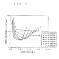
- FIGS. 2 , 3 , 4 , and 5 is a view plotting an example of the results of measuring the two dimensional electron gas concentration (2DEG concentration), the two dimensional electron gas mobility (2DEG mobility), the contact resistance, and the gate leakage current with respect to a plurality of HEMT devices 10 manufactured by variously differentiating the composition of each barrier layer 5.
- the two dimensional electron gas concentration and the two dimensional electron gas mobility are measured by the Hall effect method.
- the contact resistance is measured by a transmission line model method (TLM method).
- TLM method transmission line model method
- the gate leakage current is measured by a 2-terminal gate-drain I-V measurement method.
- FIGS. 2 through 5 also shows a criterion with respect to each characteristic value considered to be necessary for putting the HEMT device 10 into practical use (hereinafter, referred to as a "device characteristic criterion").
- this device characteristic criterion is set to be no less than 1.6 ⁇ 10 13 cm -2 for the two dimensional electron gas concentration (criterion 1), no less than 1300 cm 2 V -1 s -1 for the two dimensional electron gas mobility (criterion 2), no more than 10 ⁇ 10 -6 ⁇ cm 2 for the contact resistance (criterion 3), and no more than 1.0 ⁇ Amm -1 for the gate leakage current (criterion 4).
- the HEMT device 10 will have excellent device characteristics more than ever before by satisfying all these device characteristic criteria. It has been extremely difficult for the conventional AlGaN/GaN heterostructure to accomplish the epitaxial substrate and the HEMT device satisfying these four device characteristic criteria at the same time.
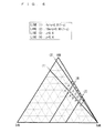
- FIG. 6 is a view of the ternary phase diagram with three components of InN, AlN, and GaN as the vertexes where the relation of the two dimensional electron gas concentration, the two dimensional electron gas mobility, the contact resistance, and the gate leakage current with the composition of the barrier layer 5 has been mapped in accordance with whether or not satisfying the above four device characteristic criteria on the basis of the results shown in FIGS. 2 and 5 .
- the HEMT devices 10 satisfying all the four device characteristic criteria are mapped with circles and the HEMT devices 10 not satisfying at least either one of the four device characteristic criteria are mapped with crosses.
- FIG. 6 indicates that the HEMT devices 10 satisfying all the four device characteristic criteria are obtained. As a result, FIG.
- the result shown in FIG. 6 indicates that the HEMT device 10 is obtained such that the two dimensional electron gas region 3e is formed with higher concentration and mobility than ever before on the heterojunction interface and the contact resistance and the gate leakage current are preferably reduced, by manufacturing the HEMT device 10 using the epitaxial substrate 10A in which the channel layer 3 is formed of GaN, the spacer layer 4 is formed of AlN, and the barrier layer 5 is formed of the composition satisfying the above range.
- the composition ratio of In in the barrier layer 5 is larger than the composition represented by the line (1) in FIG. 6 and the composition ratio of Ga in the barrier layer 5 is larger than the composition represented by the line (3) in FIG. 6 , the two dimensional electron gas concentration does not satisfy the above criteria.
- the composition ratio of In in the barrier layer 5 is smaller than the composition represented by the line (2) in FIG. 6 , the contact resistance does not satisfy the above criteria.
- the composition ratio of Ga in the barrier layer 5 is smaller than the composition represented by the line (4) in FIG. 6 , the gate leakage current increases.
- the channel layer 3, the spacer layer 4, and the barrier layer 5 include impurities.
- the channel layer 3, the spacer layer 4, and the barrier layer 5 may include oxygen atom with a concentration in the range of no less than 0.0005 at% (1 ⁇ 10 17 /cm 3 ) and no more than 0.05 at% (1 ⁇ 10 19 /cm 3 ) and carbon atom with a concentration in the range of no less than 0.0010 at% (2 ⁇ 10 7 /cm 3 ) and no more than 0.05 at% (1 ⁇ 10 19 /cm 3 )
- the concentration of each of the oxygen atom and the carbon atom may be smaller than each lower limit in the above range, it is not realistic in consideration of costs and manufacturing yield. Meanwhile, it is not preferable that the concentration of each of the oxygen atom and the carbon atom is larger than each upper limit in the above range because the crystalline quality of each layer deteriorates to the extent of causing the deterioration of the device characteristics.
- the epitaxial substrate 10A may be manufactured using a publicly known MOCVD furnace.
- the MOCVD furnace for use is constructed to be capable of supplying organic metal (MO) material gas for In, Al, and Ga (TMI, TMA, TMG), ammonia gas, hydrogen gas, and nitrogen gas into a reactor.
- MO organic metal
- a (0001) plane sapphire substrate with 2 inch diameter is prepared as a substrate 1, and the substrate 1 is placed on a susceptor provided in the reactor of the MOCVD furnace. After the atmosphere in the reactor is vacuumed, the atmosphere is regulated in a state of hydrogen/nitrogen mixed flow while the pressure in the reactor is maintained at a predetermined value of between 5 kPa and 50 kPa (e.g., 30 kPa), and then the temperature of the substrate is raised by susceptor heating.
- a susceptor temperature When a susceptor temperature reaches a predetermined temperature between 400°C and 600°C (e.g., 500°C) that is a formation temperature of the buffer layer, Ga material gas and ammonia gas are introduced into the reactor to form a GaN layer as the buffer layer 2. Alternatively, prior to this, thermal cleaning by maintaining high temperature may be performed.
- a predetermined temperature between 400°C and 600°C (e.g., 500°C) that is a formation temperature of the buffer layer.
- the susceptor temperature is maintained at a predetermined formation temperature T1 (°C) of the channel layer, and Ga material gas and ammonia gas are introduced into the reactor to form a GaN layer as the channel layer 3.
- T1 of the channel layer is a value determined within the range of 1000°C ⁇ T1 ⁇ 1200°C (e.g., 1100°C).
- an AlN layer as the spacer layer 4 is formed.
- the AlN layer is formed by maintaining the susceptor temperature at the formation temperature T1 (°C) of the channel layer, keeping the atmosphere of nitrogen gas in the reactor and setting the pressure in the reactor to be 10 kPa, and thereafter introducing Al material gas and ammonia gas into the reactor.
- the susceptor temperature is maintained at the predetermined formation temperature T2 (°C) of the barrier layer to form the atmosphere of nitrogen gas in the reactor.
- the formation temperature T2 of the barrier layer is a value determined within the range of 650°C ⁇ T2 ⁇ 900°C (e.g., 800°C).
- the pressure in the reactor is maintained to be a predetermined value between 1 kPa and 30 kPa (e.g., 10 kPa).
- the HEMT device 10 having low ohmic contact resistance and less gate leakage current (preferable Schottky contact characteristic) is obtained. This is the effect derived from the tendency that surface flatness of the barrier layer 5 is enhanced by lowering the pressure in the reactor.
- ammonia gas and organic metal material gas having a flow ratio in accordance with the composition of the barrier layer 5 are introduced into the reactor such that a so-called V/III ratio is to be a predetermined value of no less than 5000 and no more than 20000, to form an In x Al y Ga z N layer having a predetermined thickness as the barrier layer 5.
- the In x Al y Ga z N layer is formed so as to have the composition satisfying the formulas (1) to (4).
- the preferable growth rate of the barrier layer 5 is within the range of between 0.05 and 0.5 ⁇ m/h.
- the interface between the channel layer 3 and the barrier layer 5 is formed such that the average roughness is within the range of between 0.1 nm and 1 nm, and the root mean square roughness is within the range of between 0.1 nm and 1 nm.
- the barrier layer 5 nitrogen gas is used for all the bubbling gas and carrier gas for organic metal material.
- the atmosphere gas other than material gas is made of only nitrogen gas.
- hydrogen termination dangling bonds are to be nitrogen termination, and then the electron structure of the barrier layer 5 is maintained in an ideal state.
- the two dimensional electron gas with high concentration is generated in the two dimensional electron gas region 3e.
- the formation temperature T1 of the channel layer (also to be the formation temperature of the spacer layer) is determined within the range of 1000°C ⁇ T1 ⁇ 1200°C
- the formation temperature T2 of the barrier layer is determined within the range of 650°C ⁇ T2 ⁇ 900°C. Accordingly, after the channel layer 3 and the spacer layer 4 are formed, the susceptor temperature is lowered to form the barrier layer 5.
- the barrier layer is formed directly on the channel layer 3 without forming the spacer layer 4, the surface of the channel layer 3 remains exposed when the temperature is lowered, so that the surface thereof may be etched by the atmosphere gas.
- the susceptor temperature is to be lowered after the spacer layer 4 is formed, so that the spacer layer 4 functions as a protection layer for protecting the surface of the channel layer 3. This is considered to contribute to improve the two dimensional electron gas mobility.
- the barrier layer 5 has been formed, the epitaxial substrate 10A is completed.
- the epitaxial substrate 10A is obtained, and then the HEMT device 10 is manufactured by using this. It should be noted that each of the following steps is carried out by a publicly known method.
- a device isolation step is performed by etching and removing portions to be boundaries between individual devices to a depth of approximately 400 nm by a photolithography process and an RIE method. This device isolation step is only necessary for obtaining the plurality of HEMT devices 10 from a single epitaxial substrate 10A, and is not necessarily required as a step for the present invention.
- an SiO 2 film is formed on the epitaxial substrate 10A to have a predetermined thickness (e.g., 10 nm), and then, only the SiO 2 film at a portion in which the source electrode 6 and the drain electrode 7 are supposed to be formed is etched and removed by the photolithography process to form a SiO 2 pattern layer.
- a predetermined thickness e.g. 10 nm
- each of the source electrode 6 and the drain electrode 7 made of Ti/Al/Ni/Au is formed on a portion in which it is supposed to be formed, by a vacuum evaporation method and the photolithography process. Subsequently, the source electrode 6 and the drain electrode 7 are subjected to the heat treatment for several tens of seconds (e.g., 30 seconds) in the atmosphere of nitrogen gas at a predetermined temperature between 650°C and 1000°C (e.g., 850°C) in order to gain preferable ohmic quality.
- the gate electrode 8 is formed as a Schottky metal pattern.
- the HEMT device 10 is obtained by removing the rest of the SiO 2 pattern layer by the photolithography process.
- the HEMT device is accomplished so as to be equipped with all of the two dimensional electron gas with high concentration of no less than 1.6 ⁇ 10 13 cm -2 and with high mobility of no less than 1300 cm 2 V -1 s -1 , the low contact resistance of no more than 10 ⁇ 10 -6 ⁇ cm 2 , and the low gate leakage current of no more than 1.0 ⁇ Amm -1 , which have been difficult to be accomplished in the past.
- the barrier layer satisfying the above composition range is preferably formed under the atmosphere of nitrogen gas by appropriately determining the temperature, pressure, and V/III ratio.
- the spacer layer 4 is formed of AlN, it may be formed of group III nitride having the composition of Al p Ga 1-p N (wherein 0.8 ⁇ p ⁇ 1), instead of AlN. Even when the spacer layer 4 is formed in this manner, the spacer layer 4 is formed to have a larger bandgap than that of any other barrier layer 5 defined by the formulas (1) to (4). In terms of improving the concentration and mobility of the two dimensional electron gas by suppressing the alloy scattering effect, it is the most preferable to form the spacer layer 4 with AlN that is a binary system compound of Al and N, however, the same extent of effect is produced even in the case of 0.95 ⁇ p ⁇ 1.
- the channel layer 3 is formed of GaN, it may be formed of group III nitride having the composition of Al q Ga 1-q N (wherein 0 ⁇ q ⁇ 0.3), instead of GaN. Also, in this case, the composition range of the barrier layer satisfying the above four device characteristic criteria is defined in accordance with the composition of the channel layer 3.
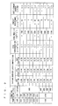
- FIG. 7 is a view showing a list of the combinations of the composition of the barrier layer 5 in manufacturing the HEMT device 10 and the results of measuring the two dimensional electron gas concentration (2DEG concentration), the two dimensional electron gas mobility (2DEG mobility), the contact resistance, and the gate leakage current with respect to the resultant HEMT devices 10.
- 2DEG concentration two dimensional electron gas concentration
- 2DEG mobility two dimensional electron gas mobility
- contact resistance the contact resistance
- the gate leakage current with respect to the resultant HEMT devices 10.
- 35 different types of the HEMT devices 10 were manufactured.
- a (0001) plane sapphire substrate with 2 inch diameter was prepared as the substrate 1 to start manufacturing the epitaxial substrate 10A used for each of the HEMT devices 10.
- the substrate 1 was placed in the reactor of the MOCVD furnace and the atmosphere in the reactor was vacuumed. Thereafter, the pressure in the reactor was set to be 30 kPa and the atmosphere was formed in a state of hydrogen/nitrogen mixed flow, and then the temperature of the substrate was raised by susceptor heating.
- the susceptor temperature was kept at this temperature for 10 minutes to perform the thermal cleaning.
- the susceptor temperature was lowered to a temperature of 500°C, Ga material gas and ammonia gas were introduced to the reactor to form the GaN layer having a thickness of 25 nm as the buffer layer 2.
- the susceptor temperature was kept at the formation temperature T1 (°C) of 1100°C, and Ga material gas and ammonia gas were introduced into the reactor to set the pressure in the reactor to be 100 kPa and form the GaN layer having a thickness of 3 ⁇ m as the channel layer 3.
- the hydrogen/nitrogen mixed gas was used for the bubbling gas and the carrier gas of the GA material gas.
- the pressure in the reactor was maintained to be 10 kPa with the susceptor temperature kept at 1100°C. Then, Al material gas and ammonia gas were introduced into the reactor to form the AlN layer having a thickness of 1 nm as the spacer layer 4.
- the hydrogen/nitrogen mixed gas was used for the bubbling gas and the carrier gas of the Al material gas.
- the temperature was kept at the formation temperature T2 (°C) of the barrier layer of 800°C and the atmosphere of nitrogen was formed in the reactor to set the pressure in the reactor to be 10 kPa.
- the organic metal material gas and ammonia gas were introduced into the reactor with the flow ratio in accordance with the composition (target composition) shown in FIG. 7 to form the In x Al y Ga z N layer having a thickness of 20 nm as the barrier layer 5.
- the nitrogen gas was used for the bubbling gas and carrier gas of the organic metal material, and the V/III ratio was to be approximately 10000.
- the susceptor temperature was lowered to nearly the room temperature to recover the atmosphere in the reactor to be atmospheric pressure. Then, the reactor was exposed to air to extract the manufactured epitaxial substrate 10A. Thereby, the epitaxial substrate 10A was obtained.
- the HEMT device 10 was manufactured using this epitaxial substrate 10A.
- the HEMT device was designed to have a gate width of 1 mm, a source-gate interval of 0.5 ⁇ m, a gate-drain interval of 7.5 ⁇ m, and a gate length of 1.5 ⁇ m.
- a portion to be a boundary between each of devices was etched and removed to a depth of approximately 400 nm by the photolithography method and RIE method.
- the SiO 2 film having a thickness of 10 nm was formed on the epitaxial substrate 10A. Then, SiO 2 film at a portion in which the source electrode 6 and the drain electrode 7 were supposed to be formed was etched and removed by the photolithography so as to obtain the SiO 2 pattern layer.
- the metal patterns made of Ti/Al/Ni/Au were formed by the vacuum evaporation method and the photolithography process, at portions in which the source electrode 6 and the drain electrode 7 were supposed to be formed, so as to form the source electrode 6 and the drain electrode 7.
- the heat treatment for 30 seconds was performed in the atmosphere of nitrogen gas at 850°C in order to obtain preferable ohmic quality of the source electrode 6 and the drain electrode 7.
- the SiO 2 film at a portion in which the gate electrode 8 was supposed to be formed was removed from the SiO 2 pattern layer by the photolithography process, and then the gate electrode 8 made of Pd/Au (each film thickness was 30/100 nm, respectively) was formed as a Schottky metal pattern in the above portion by the vacuum evaporation method and the photolithography.
- the HEMT device 10 was obtained by the above process.
- a passivation film of silicon nitride was formed by a CVD method and the photolithography process for the HEMT device 10, and then, contact holes were created on the positions corresponding to the source electrode 6, the drain electrode 7, and the gate electrode 8 of the passivation film to perform a wire bonding.
- the two dimensional electron gas concentration and mobility were measured for the resultant plurality of HEMT devices 10 by the Hall effect method.
- the contact resistance was measured by the TLM method and the gate leakage current was measured by the 2-terminal gate-drain I-V method.
- FIG. 7 shows a list of the results obtained by the above measurements.
- FIG. 2 through FIG. 5 are plots of each measurement result.
- FIG. 6 is a plot of a ternary phase diagram with InN, AlN, and GaN as vertexes in accordance with four criteria shown by FIG. 2 through FIG. 5 with respect to data of FIG. 7 .
- the epitaxial substrate having excellent characteristics was accomplished by forming the channel layer with GaN, the spacer layer with AlN, and then forming the barrier layer to satisfy the composition in the range surrounded with lines specified by the above formulas (1) to (4) in the ternary phase diagram, as shown in FIG. 6 .
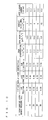
- FIG. 8 is a view showing a list of measurement results of the two dimensional electron gas concentration of each HEMT device and ways of mixing hydrogen in the process of forming the barrier layer 5, the methods being employed in manufacturing the HEMT device according to the present inventive example.
- FIG. 8 also shows the measurement results of the two dimensional electron gas concentration of the HEMT devices in the inventive example 1 with the barrier layer 5 having the same composition as the present inventive example.
- the two dimensional electron gas concentration of the HEMT device in which hydrogen was mixed into the atmosphere gas in forming the barrier layer is significantly smaller than that of the HEMT device in which hydrogen was not mixed, and the HEMT device having the two dimensional electron gas concentration exceeding the device characteristic criterion of no less than 1.6 ⁇ 10 13 cm -2 was not obtained.
- the HEMT device having the two dimensional electron gas concentration exceeding the device characteristic criterion of no less than 1.6 ⁇ 10 13 cm -2 was not obtained.
- FIG. 9 is a view showing a list of the measurement results of the above each measurement and the formation temperature of each layer employed in manufacturing the HEMT devices according to the present inventive example.
- FIG. 9 also shows the measurement results of the HEMT device according to the inventive example 1 with the barrier layer 5 having the same composition as the present inventive example. In FIG. 9 , the crosses are put to the measurement results not satisfying the device characteristic criterion.
- the HEMT device satisfying all the four device characteristic criteria is obtained by setting the formation temperature of the channel layer 3 to be no less than 1000°C and no more than 1200°C, setting the formation temperature of the spacer layer 4 to be substantially same as the formation temperature of the channel layer 3, and setting the formation temperature of the barrier layer 5 to be no less than 650°C and no more than 900°C.
- the HEMT devices were manufactured in the same procedure as the inventive example 1 other than differentiating the pressure in the reactor in forming the barrier layer 5.
- the target composition of the barrier layer 5 was In 0.06 Al 0.44 Ga 0.5 N.
- the two dimensional electron gas concentration and mobility, the contact resistance, and the gate leakage current of the resultant HEMT devices were measured.
- FIG. 10 is a view showing a list of the measurement results of the above each measurement and the pressure in the reactor employed in manufacturing the HEMT devices according to the present inventive example.
- FIG. 10 also shows the measurement results of the HEMT devices according to the inventive example 1 with the barrier layer 5 having the same composition as the present inventive example.
- the HEMT devices in which the formation temperatures of the GaN layer as the channel layer 3 and the AlN layer as the spacer layer 4 are 1100°C and the formation temperature of the In 0.06 Al 0.44 Ga 0.5 N layer as the barrier layer 5 is 800°C correspond to them.
- the HEMT device satisfying all the four device characteristic criteria is obtained by setting the pressure in the reactor in forming the barrier layer 5 to be no less than 1 kPa and no more than 30 kPa. It has been also confirmed that the HEMT device having lower ohmic contact resistance and less gate leakage current (preferable Schottky contact characteristic) is obtained by setting the pressure in the reactor to be no less than 1 kPa and no more than 20 kPa.
- the HEMT devices were manufactured by the same procedure as the inventive example 1 other than differentiating the V/III ratio in forming the barrier layer 5.
- the target composition of the barrier layer 5 was In 0.06 Al 0.44 Ga 0.5 N.
- the two dimensional electron gas concentration and mobility, the contact resistance, and the gate leakage current of the resultant HEMT devices were measured.
- the surface root mean square roughness (Rms) of the epitaxial substrate obtained in the process of manufacturing the HEMT device was measured by AFM.
- FIG. 11 is a view showing a list of the measurement results of the above each measurement and the V/III ratio in forming the barrier layer 5 employed in manufacturing the HEMT devices according to the present inventive example.
- FIG. 11 is a view showing a list of the measurement results of the above each measurement and the V/III ratio in forming the barrier layer 5 employed in manufacturing the HEMT devices according to the present inventive example.
- FIG. 11 also shows the measurement results of the HEMT devices according to the inventive example 1 with the barrier layer 5 having the same composition as the present inventive example. Specifically, the HEMT devices having the V/III ratio of 10000 correspond to them.
- FIG. 12 is a view showing the obtained AFM images for the epitaxial substrate of a part of the HEMT devices.
- FIG. 12 (a) is the AFM image when the V/III ratio is 10000
- FIG. 12 (b) is the AFM image when the V/III ratio is 40000.
- the HEMT device satisfying all the four device characteristic criteria is obtained by setting the V/III ratio in forming the barrier layer 5 to be no less than 5000 and no more than 20000.
- the improvement of the surface flatness (reducing the surface root means square roughness) by appropriately selecting the V/III ratio is considered to be effective in improving the characteristics of the HEMT devices.
Landscapes
- Chemical & Material Sciences (AREA)
- Engineering & Computer Science (AREA)
- Crystallography & Structural Chemistry (AREA)
- Materials Engineering (AREA)
- Metallurgy (AREA)
- Organic Chemistry (AREA)
- Inorganic Chemistry (AREA)
- Chemical Kinetics & Catalysis (AREA)
- General Chemical & Material Sciences (AREA)
- Junction Field-Effect Transistors (AREA)
- Chemical Vapour Deposition (AREA)
- Recrystallisation Techniques (AREA)
Applications Claiming Priority (1)
| Application Number | Priority Date | Filing Date | Title |
|---|---|---|---|
| JP2009115582A JP5562579B2 (ja) | 2009-05-12 | 2009-05-12 | 半導体素子用エピタキシャル基板の作製方法 |
Publications (3)
| Publication Number | Publication Date |
|---|---|
| EP2251464A2 true EP2251464A2 (de) | 2010-11-17 |
| EP2251464A3 EP2251464A3 (de) | 2011-01-26 |
| EP2251464B1 EP2251464B1 (de) | 2019-01-16 |
Family
ID=42358651
Family Applications (1)
| Application Number | Title | Priority Date | Filing Date |
|---|---|---|---|
| EP10250839.7A Not-in-force EP2251464B1 (de) | 2009-05-12 | 2010-04-27 | Epitaxiesubstrat für Halbleiterbauelement, Halbleiterbauelement und Verfahren zur Herstellung eines Epitaxiesubstrats für ein Halbleiterbauelement |
Country Status (3)
| Country | Link |
|---|---|
| US (1) | US9382641B2 (de) |
| EP (1) | EP2251464B1 (de) |
| JP (1) | JP5562579B2 (de) |
Cited By (4)
| Publication number | Priority date | Publication date | Assignee | Title |
|---|---|---|---|---|
| CN106601787A (zh) * | 2016-12-01 | 2017-04-26 | 北京大学 | 一种InxAlyGa1‑x‑yN/GaN异质结构外延方法 |
| US10483388B2 (en) | 2017-06-20 | 2019-11-19 | SCIOCS COMPANY LlMITED | Nitride semiconductor epitaxial substrate and semiconductor device |
| EP3598504A1 (de) * | 2018-07-19 | 2020-01-22 | Sciocs Company Limited | Epitaktisches nitrid-halbleitersubstrat und halbleiterbauelement |
| CN115142126B (zh) * | 2022-06-30 | 2023-09-26 | 江苏第三代半导体研究院有限公司 | 一种低背景浓度氮化镓外延结构的制备方法及其外延结构 |
Families Citing this family (7)
| Publication number | Priority date | Publication date | Assignee | Title |
|---|---|---|---|---|
| US8659030B2 (en) * | 2011-02-28 | 2014-02-25 | International Rectifier Corporation | III-nitride heterojunction devices having a multilayer spacer |
| WO2013109884A1 (en) * | 2012-01-18 | 2013-07-25 | Iqe Kc, Llc | Iiii -n- based double heterostructure field effect transistor and method of forming the same |
| US20180061975A1 (en) | 2016-08-24 | 2018-03-01 | Rohm Co., Ltd. | Nitride semiconductor device and nitride semiconductor package |
| JP7025853B2 (ja) * | 2016-08-24 | 2022-02-25 | ローム株式会社 | 窒化物半導体デバイスおよび窒化物半導体パッケージ |
| CN111164733B (zh) * | 2017-07-20 | 2024-03-19 | 斯维甘公司 | 用于高电子迁移率晶体管的异质结构及其生产方法 |
| JP7032641B2 (ja) | 2018-01-11 | 2022-03-09 | 富士通株式会社 | 化合物半導体装置及びその製造方法 |
| CN116240630A (zh) * | 2018-08-01 | 2023-06-09 | 出光兴产株式会社 | 晶体化合物、氧化物烧结体、溅射靶、晶质及无定形氧化物薄膜、薄膜晶体管及电子设备 |
Citations (1)
| Publication number | Priority date | Publication date | Assignee | Title |
|---|---|---|---|---|
| JP2007324263A (ja) | 2006-05-31 | 2007-12-13 | Matsushita Electric Ind Co Ltd | 電界効果トランジスタ及びその製造方法 |
Family Cites Families (36)
| Publication number | Priority date | Publication date | Assignee | Title |
|---|---|---|---|---|
| JPH11204885A (ja) * | 1998-01-08 | 1999-07-30 | Sony Corp | 窒化物系iii−v族化合物半導体層の成長方法および半導体装置の製造方法 |
| JP2000012834A (ja) * | 1998-06-22 | 2000-01-14 | Mitsubishi Electric Corp | ダブルヘテロ構造高電子移動度トランジスタおよびその製造方法、並びに該トランジスタ用ウエハ |
| JP3209270B2 (ja) * | 1999-01-29 | 2001-09-17 | 日本電気株式会社 | ヘテロ接合電界効果トランジスタ |
| JP4022708B2 (ja) * | 2000-06-29 | 2007-12-19 | 日本電気株式会社 | 半導体装置 |
| JP4220683B2 (ja) * | 2001-03-27 | 2009-02-04 | パナソニック株式会社 | 半導体装置 |
| JP2003178976A (ja) * | 2001-12-12 | 2003-06-27 | Matsushita Electric Ind Co Ltd | 半導体装置およびその製造方法 |
| JP3977659B2 (ja) * | 2002-02-21 | 2007-09-19 | 沖電気工業株式会社 | ヘテロ接合電界効果トランジスタ |
| US8089097B2 (en) * | 2002-12-27 | 2012-01-03 | Momentive Performance Materials Inc. | Homoepitaxial gallium-nitride-based electronic devices and method for producing same |
| JP2004311492A (ja) * | 2003-04-02 | 2004-11-04 | Matsushita Electric Ind Co Ltd | ヘテロ接合電界効果型トランジスタ |
| SG135924A1 (en) * | 2003-04-02 | 2007-10-29 | Sumitomo Electric Industries | Nitride-based semiconductor epitaxial substrate, method of manufacturing the same, and hemt substrate |
| US7279697B2 (en) * | 2003-12-05 | 2007-10-09 | International Rectifier Corporation | Field effect transistor with enhanced insulator structure |
| US7170111B2 (en) * | 2004-02-05 | 2007-01-30 | Cree, Inc. | Nitride heterojunction transistors having charge-transfer induced energy barriers and methods of fabricating the same |
| JP4748945B2 (ja) * | 2004-03-26 | 2011-08-17 | 日本碍子株式会社 | トランジスタ素子の作製方法 |
| JP2006032911A (ja) * | 2004-06-15 | 2006-02-02 | Ngk Insulators Ltd | 半導体積層構造、半導体素子およびhemt素子 |
| JP5248743B2 (ja) * | 2004-06-30 | 2013-07-31 | アイメック | 半導体装置および半導体装置の製造方法 |
| EP2273553B1 (de) * | 2004-06-30 | 2020-02-12 | IMEC vzw | Verfahren zur Herstellung von AlGaN/GaN HEMT Anordnungen |
| US7547928B2 (en) | 2004-06-30 | 2009-06-16 | Interuniversitair Microelektronica Centrum (Imec) | AlGaN/GaN high electron mobility transistor devices |
| WO2006022453A1 (ja) | 2004-08-27 | 2006-03-02 | National Institute Of Information And Communications Technology, Incorporated Administrative Agency | GaN系電界効果トランジスタおよびその製造方法 |
| US20060226442A1 (en) * | 2005-04-07 | 2006-10-12 | An-Ping Zhang | GaN-based high electron mobility transistor and method for making the same |
| US7544963B2 (en) * | 2005-04-29 | 2009-06-09 | Cree, Inc. | Binary group III-nitride based high electron mobility transistors |
| US20070018198A1 (en) * | 2005-07-20 | 2007-01-25 | Brandes George R | High electron mobility electronic device structures comprising native substrates and methods for making the same |
| JP4908856B2 (ja) * | 2006-01-24 | 2012-04-04 | 日本電信電話株式会社 | 半導体装置とその製造法 |
| JP5207598B2 (ja) * | 2006-05-24 | 2013-06-12 | パナソニック株式会社 | 窒化物半導体材料、半導体素子およびその製造方法 |
| US8399911B2 (en) * | 2006-06-07 | 2013-03-19 | Imec | Enhancement mode field effect device and the method of production thereof |
| EP2087511B1 (de) * | 2006-11-21 | 2015-03-18 | Imec | Oberflächenbehandlung und passivierung von aigan/gan hemt |
| JP2008205029A (ja) * | 2007-02-16 | 2008-09-04 | Toshiba Corp | 窒化物半導体装置 |
| US7501670B2 (en) * | 2007-03-20 | 2009-03-10 | Velox Semiconductor Corporation | Cascode circuit employing a depletion-mode, GaN-based FET |
| JP5292716B2 (ja) * | 2007-03-30 | 2013-09-18 | 富士通株式会社 | 化合物半導体装置 |
| TWI512831B (zh) * | 2007-06-01 | 2015-12-11 | 美國加利福尼亞大學董事會 | 氮化鎵p型/氮化鋁鎵/氮化鋁/氮化鎵增強型場效電晶體 |
| JP5245305B2 (ja) * | 2007-07-06 | 2013-07-24 | サンケン電気株式会社 | 電界効果半導体装置及びその製造方法 |
| JP5100413B2 (ja) * | 2008-01-24 | 2012-12-19 | 株式会社東芝 | 半導体装置およびその製造方法 |
| US8309987B2 (en) * | 2008-07-15 | 2012-11-13 | Imec | Enhancement mode semiconductor device |
| JP2010040828A (ja) * | 2008-08-06 | 2010-02-18 | Nippon Telegr & Teleph Corp <Ntt> | 窒化物半導体装置 |
| DE112010001556B4 (de) * | 2009-04-08 | 2022-01-27 | Efficient Power Conversion Corporation | Rückdiffusionsunterdrückende Strukturen |
| US8431960B2 (en) * | 2009-04-08 | 2013-04-30 | Efficient Power Conversion Corporation | Dopant diffusion modulation in GaN buffer layers |
| US20100270591A1 (en) * | 2009-04-27 | 2010-10-28 | University Of Seoul Industry Cooperation Foundation | High-electron mobility transistor |
-
2009
- 2009-05-12 JP JP2009115582A patent/JP5562579B2/ja not_active Expired - Fee Related
-
2010
- 2010-04-26 US US12/767,041 patent/US9382641B2/en active Active
- 2010-04-27 EP EP10250839.7A patent/EP2251464B1/de not_active Not-in-force
Patent Citations (1)
| Publication number | Priority date | Publication date | Assignee | Title |
|---|---|---|---|---|
| JP2007324263A (ja) | 2006-05-31 | 2007-12-13 | Matsushita Electric Ind Co Ltd | 電界効果トランジスタ及びその製造方法 |
Non-Patent Citations (4)
| Title |
|---|
| MAKOTO MIYOSHI ET AL.: "Characterization of Different-Al-Content AIGaN/GaN Heterostructures and High-Electron-Mobility Transistors Grown on 100-mm-Diameter Sapphire Substrates by Metalorganic Vapor Phase Epitaxy", JPN. J. APPL. PHYS., vol. 43, no. 12, 2004, pages 7939 - 7943 |
| STACIA KELLER; YI-FENG WU; GIACINTA PARISH; NAIQIAN ZIANG; JANE J. XU; BERND P. KELLER; STEVEN P. DENBAARS; UMESH K; MISHRA: "Gallium Nitride Based High Power Heterojunction Field Effect Transistors: process Development and Present Status at UCSB", IEEE TRANS. ELECTRON DEVICES, vol. 48, 2001, pages 552 |
| TOSHIHIDE KIKKAWA: "Highly Reliable 250 W High Electron Mobility Transistor Power Amplifier", JPN. J. APPL. PHYS., vol. 44, no. 7A, 2005, pages 4896 - 4901 |
| YANG LIU ET AL.: "Novel Quaternary AIInGaN/GaN Heterostructure Field Effect Transistors on Sapphire Substrate", JPN. J. APPL. PHYS., vol. 45, no. 7, 2005, pages 5728 - 5731 |
Cited By (4)
| Publication number | Priority date | Publication date | Assignee | Title |
|---|---|---|---|---|
| CN106601787A (zh) * | 2016-12-01 | 2017-04-26 | 北京大学 | 一种InxAlyGa1‑x‑yN/GaN异质结构外延方法 |
| US10483388B2 (en) | 2017-06-20 | 2019-11-19 | SCIOCS COMPANY LlMITED | Nitride semiconductor epitaxial substrate and semiconductor device |
| EP3598504A1 (de) * | 2018-07-19 | 2020-01-22 | Sciocs Company Limited | Epitaktisches nitrid-halbleitersubstrat und halbleiterbauelement |
| CN115142126B (zh) * | 2022-06-30 | 2023-09-26 | 江苏第三代半导体研究院有限公司 | 一种低背景浓度氮化镓外延结构的制备方法及其外延结构 |
Also Published As
| Publication number | Publication date |
|---|---|
| US9382641B2 (en) | 2016-07-05 |
| EP2251464A3 (de) | 2011-01-26 |
| JP2010267658A (ja) | 2010-11-25 |
| EP2251464B1 (de) | 2019-01-16 |
| US20100289029A1 (en) | 2010-11-18 |
| JP5562579B2 (ja) | 2014-07-30 |
Similar Documents
| Publication | Publication Date | Title |
|---|---|---|
| EP2251464B1 (de) | Epitaxiesubstrat für Halbleiterbauelement, Halbleiterbauelement und Verfahren zur Herstellung eines Epitaxiesubstrats für ein Halbleiterbauelement | |
| EP3067921B1 (de) | Verfahren zur herstellung eines epitaktischen substrats für ein halbleiterbauelement | |
| US10410859B2 (en) | Epitaxial substrate for semiconductor elements, semiconductor element, and manufacturing method for epitaxial substrates for semiconductor elements | |
| EP2290675B1 (de) | Epitaxiesubstrat für Halbleiterbauelement, Halbleiterbauelement und Verfahren zur Herstellung eines Epitaxiesubstrats für ein Halbleiterbauelement | |
| EP2290696B1 (de) | Epitaxiesubstrat für Halbleiterbauelement, Halbleiterbauelement und Verfahren zur Herstellung eines Epitaxiesubstrats für ein Halbleiterbauelement | |
| JP5758880B2 (ja) | 半導体素子用エピタキシャル基板、半導体素子、および半導体素子用エピタキシャル基板の作製方法 | |
| EP2538434A1 (de) | Epitaktisches substrat und herstellungsverfahren dafür | |
| KR101933230B1 (ko) | 반도체 소자, hemt 소자, 및 반도체 소자의 제조 방법 | |
| JPWO2009119357A1 (ja) | 半導体素子用エピタキシャル基板、半導体素子、および半導体素子用エピタキシャル基板の作製方法 | |
| EP2296172B1 (de) | Epitaxialsubstrate für Halbleiterbauelement, Schottky-Übergangsstruktur und Verfahren zur Leckstromunterdrückung für Schottky-Übergangsstruktur | |
| US10629688B2 (en) | Epitaxial substrate for semiconductor elements, semiconductor element, and manufacturing method for epitaxial substrates for semiconductor elements | |
| JP4972879B2 (ja) | 電界効果トランジスタ、半導体素子、及びエピタキシャル基板 |
Legal Events
| Date | Code | Title | Description |
|---|---|---|---|
| PUAI | Public reference made under article 153(3) epc to a published international application that has entered the european phase |
Free format text: ORIGINAL CODE: 0009012 |
|
| AK | Designated contracting states |
Kind code of ref document: A2 Designated state(s): AT BE BG CH CY CZ DE DK EE ES FI FR GB GR HR HU IE IS IT LI LT LU LV MC MK MT NL NO PL PT RO SE SI SK SM TR |
|
| AX | Request for extension of the european patent |
Extension state: AL BA ME RS |
|
| PUAL | Search report despatched |
Free format text: ORIGINAL CODE: 0009013 |
|
| AK | Designated contracting states |
Kind code of ref document: A3 Designated state(s): AT BE BG CH CY CZ DE DK EE ES FI FR GB GR HR HU IE IS IT LI LT LU LV MC MK MT NL NO PL PT RO SE SI SK SM TR |
|
| AX | Request for extension of the european patent |
Extension state: AL BA ME RS |
|
| 17P | Request for examination filed |
Effective date: 20110719 |
|
| STAA | Information on the status of an ep patent application or granted ep patent |
Free format text: STATUS: EXAMINATION IS IN PROGRESS |
|
| 17Q | First examination report despatched |
Effective date: 20170127 |
|
| GRAP | Despatch of communication of intention to grant a patent |
Free format text: ORIGINAL CODE: EPIDOSNIGR1 |
|
| STAA | Information on the status of an ep patent application or granted ep patent |
Free format text: STATUS: GRANT OF PATENT IS INTENDED |
|
| INTG | Intention to grant announced |
Effective date: 20180831 |
|
| GRAS | Grant fee paid |
Free format text: ORIGINAL CODE: EPIDOSNIGR3 |
|
| GRAA | (expected) grant |
Free format text: ORIGINAL CODE: 0009210 |
|
| STAA | Information on the status of an ep patent application or granted ep patent |
Free format text: STATUS: THE PATENT HAS BEEN GRANTED |
|
| AK | Designated contracting states |
Kind code of ref document: B1 Designated state(s): AT BE BG CH CY CZ DE DK EE ES FI FR GB GR HR HU IE IS IT LI LT LU LV MC MK MT NL NO PL PT RO SE SI SK SM TR |
|
| REG | Reference to a national code |
Ref country code: GB Ref legal event code: FG4D |
|
| REG | Reference to a national code |
Ref country code: CH Ref legal event code: EP |
|
| REG | Reference to a national code |
Ref country code: IE Ref legal event code: FG4D |
|
| REG | Reference to a national code |
Ref country code: DE Ref legal event code: R096 Ref document number: 602010056558 Country of ref document: DE |
|
| REG | Reference to a national code |
Ref country code: AT Ref legal event code: REF Ref document number: 1089767 Country of ref document: AT Kind code of ref document: T Effective date: 20190215 |
|
| REG | Reference to a national code |
Ref country code: NL Ref legal event code: MP Effective date: 20190116 |
|
| REG | Reference to a national code |
Ref country code: LT Ref legal event code: MG4D |
|
| PG25 | Lapsed in a contracting state [announced via postgrant information from national office to epo] |
Ref country code: NL Free format text: LAPSE BECAUSE OF FAILURE TO SUBMIT A TRANSLATION OF THE DESCRIPTION OR TO PAY THE FEE WITHIN THE PRESCRIBED TIME-LIMIT Effective date: 20190116 |
|
| REG | Reference to a national code |
Ref country code: AT Ref legal event code: MK05 Ref document number: 1089767 Country of ref document: AT Kind code of ref document: T Effective date: 20190116 |
|
| PG25 | Lapsed in a contracting state [announced via postgrant information from national office to epo] |
Ref country code: PT Free format text: LAPSE BECAUSE OF FAILURE TO SUBMIT A TRANSLATION OF THE DESCRIPTION OR TO PAY THE FEE WITHIN THE PRESCRIBED TIME-LIMIT Effective date: 20190516 Ref country code: ES Free format text: LAPSE BECAUSE OF FAILURE TO SUBMIT A TRANSLATION OF THE DESCRIPTION OR TO PAY THE FEE WITHIN THE PRESCRIBED TIME-LIMIT Effective date: 20190116 Ref country code: SE Free format text: LAPSE BECAUSE OF FAILURE TO SUBMIT A TRANSLATION OF THE DESCRIPTION OR TO PAY THE FEE WITHIN THE PRESCRIBED TIME-LIMIT Effective date: 20190116 Ref country code: NO Free format text: LAPSE BECAUSE OF FAILURE TO SUBMIT A TRANSLATION OF THE DESCRIPTION OR TO PAY THE FEE WITHIN THE PRESCRIBED TIME-LIMIT Effective date: 20190416 Ref country code: FI Free format text: LAPSE BECAUSE OF FAILURE TO SUBMIT A TRANSLATION OF THE DESCRIPTION OR TO PAY THE FEE WITHIN THE PRESCRIBED TIME-LIMIT Effective date: 20190116 Ref country code: PL Free format text: LAPSE BECAUSE OF FAILURE TO SUBMIT A TRANSLATION OF THE DESCRIPTION OR TO PAY THE FEE WITHIN THE PRESCRIBED TIME-LIMIT Effective date: 20190116 Ref country code: LT Free format text: LAPSE BECAUSE OF FAILURE TO SUBMIT A TRANSLATION OF THE DESCRIPTION OR TO PAY THE FEE WITHIN THE PRESCRIBED TIME-LIMIT Effective date: 20190116 |
|
| PG25 | Lapsed in a contracting state [announced via postgrant information from national office to epo] |
Ref country code: BG Free format text: LAPSE BECAUSE OF FAILURE TO SUBMIT A TRANSLATION OF THE DESCRIPTION OR TO PAY THE FEE WITHIN THE PRESCRIBED TIME-LIMIT Effective date: 20190416 Ref country code: GR Free format text: LAPSE BECAUSE OF FAILURE TO SUBMIT A TRANSLATION OF THE DESCRIPTION OR TO PAY THE FEE WITHIN THE PRESCRIBED TIME-LIMIT Effective date: 20190417 Ref country code: LV Free format text: LAPSE BECAUSE OF FAILURE TO SUBMIT A TRANSLATION OF THE DESCRIPTION OR TO PAY THE FEE WITHIN THE PRESCRIBED TIME-LIMIT Effective date: 20190116 Ref country code: HR Free format text: LAPSE BECAUSE OF FAILURE TO SUBMIT A TRANSLATION OF THE DESCRIPTION OR TO PAY THE FEE WITHIN THE PRESCRIBED TIME-LIMIT Effective date: 20190116 Ref country code: IS Free format text: LAPSE BECAUSE OF FAILURE TO SUBMIT A TRANSLATION OF THE DESCRIPTION OR TO PAY THE FEE WITHIN THE PRESCRIBED TIME-LIMIT Effective date: 20190516 |
|
| REG | Reference to a national code |
Ref country code: DE Ref legal event code: R097 Ref document number: 602010056558 Country of ref document: DE |
|
| PG25 | Lapsed in a contracting state [announced via postgrant information from national office to epo] |
Ref country code: IT Free format text: LAPSE BECAUSE OF FAILURE TO SUBMIT A TRANSLATION OF THE DESCRIPTION OR TO PAY THE FEE WITHIN THE PRESCRIBED TIME-LIMIT Effective date: 20190116 Ref country code: RO Free format text: LAPSE BECAUSE OF FAILURE TO SUBMIT A TRANSLATION OF THE DESCRIPTION OR TO PAY THE FEE WITHIN THE PRESCRIBED TIME-LIMIT Effective date: 20190116 Ref country code: SK Free format text: LAPSE BECAUSE OF FAILURE TO SUBMIT A TRANSLATION OF THE DESCRIPTION OR TO PAY THE FEE WITHIN THE PRESCRIBED TIME-LIMIT Effective date: 20190116 Ref country code: CZ Free format text: LAPSE BECAUSE OF FAILURE TO SUBMIT A TRANSLATION OF THE DESCRIPTION OR TO PAY THE FEE WITHIN THE PRESCRIBED TIME-LIMIT Effective date: 20190116 Ref country code: EE Free format text: LAPSE BECAUSE OF FAILURE TO SUBMIT A TRANSLATION OF THE DESCRIPTION OR TO PAY THE FEE WITHIN THE PRESCRIBED TIME-LIMIT Effective date: 20190116 Ref country code: AT Free format text: LAPSE BECAUSE OF FAILURE TO SUBMIT A TRANSLATION OF THE DESCRIPTION OR TO PAY THE FEE WITHIN THE PRESCRIBED TIME-LIMIT Effective date: 20190116 Ref country code: DK Free format text: LAPSE BECAUSE OF FAILURE TO SUBMIT A TRANSLATION OF THE DESCRIPTION OR TO PAY THE FEE WITHIN THE PRESCRIBED TIME-LIMIT Effective date: 20190116 |
|
| PLBE | No opposition filed within time limit |
Free format text: ORIGINAL CODE: 0009261 |
|
| STAA | Information on the status of an ep patent application or granted ep patent |
Free format text: STATUS: NO OPPOSITION FILED WITHIN TIME LIMIT |
|
| PG25 | Lapsed in a contracting state [announced via postgrant information from national office to epo] |
Ref country code: SM Free format text: LAPSE BECAUSE OF FAILURE TO SUBMIT A TRANSLATION OF THE DESCRIPTION OR TO PAY THE FEE WITHIN THE PRESCRIBED TIME-LIMIT Effective date: 20190116 |
|
| REG | Reference to a national code |
Ref country code: CH Ref legal event code: PL |
|
| REG | Reference to a national code |
Ref country code: BE Ref legal event code: MM Effective date: 20190430 |
|
| 26N | No opposition filed |
Effective date: 20191017 |
|
| GBPC | Gb: european patent ceased through non-payment of renewal fee |
Effective date: 20190427 |
|
| PG25 | Lapsed in a contracting state [announced via postgrant information from national office to epo] |
Ref country code: MC Free format text: LAPSE BECAUSE OF FAILURE TO SUBMIT A TRANSLATION OF THE DESCRIPTION OR TO PAY THE FEE WITHIN THE PRESCRIBED TIME-LIMIT Effective date: 20190116 Ref country code: LU Free format text: LAPSE BECAUSE OF NON-PAYMENT OF DUE FEES Effective date: 20190427 |
|
| PG25 | Lapsed in a contracting state [announced via postgrant information from national office to epo] |
Ref country code: CH Free format text: LAPSE BECAUSE OF NON-PAYMENT OF DUE FEES Effective date: 20190430 Ref country code: LI Free format text: LAPSE BECAUSE OF NON-PAYMENT OF DUE FEES Effective date: 20190430 Ref country code: GB Free format text: LAPSE BECAUSE OF NON-PAYMENT OF DUE FEES Effective date: 20190427 |
|
| PG25 | Lapsed in a contracting state [announced via postgrant information from national office to epo] |
Ref country code: SI Free format text: LAPSE BECAUSE OF FAILURE TO SUBMIT A TRANSLATION OF THE DESCRIPTION OR TO PAY THE FEE WITHIN THE PRESCRIBED TIME-LIMIT Effective date: 20190116 Ref country code: FR Free format text: LAPSE BECAUSE OF NON-PAYMENT OF DUE FEES Effective date: 20190430 Ref country code: BE Free format text: LAPSE BECAUSE OF NON-PAYMENT OF DUE FEES Effective date: 20190430 |
|
| PG25 | Lapsed in a contracting state [announced via postgrant information from national office to epo] |
Ref country code: TR Free format text: LAPSE BECAUSE OF FAILURE TO SUBMIT A TRANSLATION OF THE DESCRIPTION OR TO PAY THE FEE WITHIN THE PRESCRIBED TIME-LIMIT Effective date: 20190116 |
|
| PG25 | Lapsed in a contracting state [announced via postgrant information from national office to epo] |
Ref country code: IE Free format text: LAPSE BECAUSE OF NON-PAYMENT OF DUE FEES Effective date: 20190427 |
|
| PG25 | Lapsed in a contracting state [announced via postgrant information from national office to epo] |
Ref country code: CY Free format text: LAPSE BECAUSE OF FAILURE TO SUBMIT A TRANSLATION OF THE DESCRIPTION OR TO PAY THE FEE WITHIN THE PRESCRIBED TIME-LIMIT Effective date: 20190116 |
|
| PG25 | Lapsed in a contracting state [announced via postgrant information from national office to epo] |
Ref country code: MT Free format text: LAPSE BECAUSE OF FAILURE TO SUBMIT A TRANSLATION OF THE DESCRIPTION OR TO PAY THE FEE WITHIN THE PRESCRIBED TIME-LIMIT Effective date: 20190116 Ref country code: HU Free format text: LAPSE BECAUSE OF FAILURE TO SUBMIT A TRANSLATION OF THE DESCRIPTION OR TO PAY THE FEE WITHIN THE PRESCRIBED TIME-LIMIT; INVALID AB INITIO Effective date: 20100427 |
|
| PG25 | Lapsed in a contracting state [announced via postgrant information from national office to epo] |
Ref country code: MK Free format text: LAPSE BECAUSE OF FAILURE TO SUBMIT A TRANSLATION OF THE DESCRIPTION OR TO PAY THE FEE WITHIN THE PRESCRIBED TIME-LIMIT Effective date: 20190116 |
|
| PGFP | Annual fee paid to national office [announced via postgrant information from national office to epo] |
Ref country code: DE Payment date: 20240306 Year of fee payment: 15 |
|
| REG | Reference to a national code |
Ref country code: DE Ref legal event code: R119 Ref document number: 602010056558 Country of ref document: DE |
|
| PG25 | Lapsed in a contracting state [announced via postgrant information from national office to epo] |
Ref country code: DE Free format text: LAPSE BECAUSE OF NON-PAYMENT OF DUE FEES Effective date: 20251104 |