EP2251966B1 - Convertisseur CC-CC avec modes de conduction discontinue et continue - Google Patents
Convertisseur CC-CC avec modes de conduction discontinue et continue Download PDFInfo
- Publication number
- EP2251966B1 EP2251966B1 EP09160037A EP09160037A EP2251966B1 EP 2251966 B1 EP2251966 B1 EP 2251966B1 EP 09160037 A EP09160037 A EP 09160037A EP 09160037 A EP09160037 A EP 09160037A EP 2251966 B1 EP2251966 B1 EP 2251966B1
- Authority
- EP
- European Patent Office
- Prior art keywords
- threshold
- converter
- switch
- inductor current
- current
- Prior art date
- Legal status (The legal status is an assumption and is not a legal conclusion. Google has not performed a legal analysis and makes no representation as to the accuracy of the status listed.)
- Not-in-force
Links
- 230000005415 magnetization Effects 0.000 claims abstract description 24
- 230000005347 demagnetization Effects 0.000 claims abstract description 19
- 230000001939 inductive effect Effects 0.000 claims abstract description 11
- 230000007423 decrease Effects 0.000 claims abstract description 8
- 238000000034 method Methods 0.000 claims description 27
- 230000010355 oscillation Effects 0.000 claims description 10
- 230000001419 dependent effect Effects 0.000 abstract description 8
- 230000008901 benefit Effects 0.000 description 6
- 238000005259 measurement Methods 0.000 description 4
- 238000013461 design Methods 0.000 description 3
- 239000003990 capacitor Substances 0.000 description 2
- 230000000694 effects Effects 0.000 description 2
- 230000001052 transient effect Effects 0.000 description 2
- 230000007704 transition Effects 0.000 description 2
- 230000000903 blocking effect Effects 0.000 description 1
- 238000012986 modification Methods 0.000 description 1
- 230000004048 modification Effects 0.000 description 1
- 238000012544 monitoring process Methods 0.000 description 1
- 230000003287 optical effect Effects 0.000 description 1
- 230000002265 prevention Effects 0.000 description 1
- 230000001960 triggered effect Effects 0.000 description 1
Images

Classifications
-
- H—ELECTRICITY
- H02—GENERATION; CONVERSION OR DISTRIBUTION OF ELECTRIC POWER
- H02M—APPARATUS FOR CONVERSION BETWEEN AC AND AC, BETWEEN AC AND DC, OR BETWEEN DC AND DC, AND FOR USE WITH MAINS OR SIMILAR POWER SUPPLY SYSTEMS; CONVERSION OF DC OR AC INPUT POWER INTO SURGE OUTPUT POWER; CONTROL OR REGULATION THEREOF
- H02M3/00—Conversion of DC power input into DC power output
- H02M3/02—Conversion of DC power input into DC power output without intermediate conversion into AC
- H02M3/04—Conversion of DC power input into DC power output without intermediate conversion into AC by static converters
- H02M3/10—Conversion of DC power input into DC power output without intermediate conversion into AC by static converters using discharge tubes with control electrode or semiconductor devices with control electrode
- H02M3/145—Conversion of DC power input into DC power output without intermediate conversion into AC by static converters using discharge tubes with control electrode or semiconductor devices with control electrode using devices of a triode or transistor type requiring continuous application of a control signal
- H02M3/155—Conversion of DC power input into DC power output without intermediate conversion into AC by static converters using discharge tubes with control electrode or semiconductor devices with control electrode using devices of a triode or transistor type requiring continuous application of a control signal using semiconductor devices only
- H02M3/156—Conversion of DC power input into DC power output without intermediate conversion into AC by static converters using discharge tubes with control electrode or semiconductor devices with control electrode using devices of a triode or transistor type requiring continuous application of a control signal using semiconductor devices only with automatic control of output voltage or current, e.g. switching regulators
-
- H—ELECTRICITY
- H02—GENERATION; CONVERSION OR DISTRIBUTION OF ELECTRIC POWER
- H02M—APPARATUS FOR CONVERSION BETWEEN AC AND AC, BETWEEN AC AND DC, OR BETWEEN DC AND DC, AND FOR USE WITH MAINS OR SIMILAR POWER SUPPLY SYSTEMS; CONVERSION OF DC OR AC INPUT POWER INTO SURGE OUTPUT POWER; CONTROL OR REGULATION THEREOF
- H02M3/00—Conversion of DC power input into DC power output
- H02M3/02—Conversion of DC power input into DC power output without intermediate conversion into AC
- H02M3/04—Conversion of DC power input into DC power output without intermediate conversion into AC by static converters
- H02M3/10—Conversion of DC power input into DC power output without intermediate conversion into AC by static converters using discharge tubes with control electrode or semiconductor devices with control electrode
- H02M3/145—Conversion of DC power input into DC power output without intermediate conversion into AC by static converters using discharge tubes with control electrode or semiconductor devices with control electrode using devices of a triode or transistor type requiring continuous application of a control signal
- H02M3/155—Conversion of DC power input into DC power output without intermediate conversion into AC by static converters using discharge tubes with control electrode or semiconductor devices with control electrode using devices of a triode or transistor type requiring continuous application of a control signal using semiconductor devices only
- H02M3/156—Conversion of DC power input into DC power output without intermediate conversion into AC by static converters using discharge tubes with control electrode or semiconductor devices with control electrode using devices of a triode or transistor type requiring continuous application of a control signal using semiconductor devices only with automatic control of output voltage or current, e.g. switching regulators
- H02M3/158—Conversion of DC power input into DC power output without intermediate conversion into AC by static converters using discharge tubes with control electrode or semiconductor devices with control electrode using devices of a triode or transistor type requiring continuous application of a control signal using semiconductor devices only with automatic control of output voltage or current, e.g. switching regulators including plural semiconductor devices as final control devices for a single load
-
- H—ELECTRICITY
- H02—GENERATION; CONVERSION OR DISTRIBUTION OF ELECTRIC POWER
- H02M—APPARATUS FOR CONVERSION BETWEEN AC AND AC, BETWEEN AC AND DC, OR BETWEEN DC AND DC, AND FOR USE WITH MAINS OR SIMILAR POWER SUPPLY SYSTEMS; CONVERSION OF DC OR AC INPUT POWER INTO SURGE OUTPUT POWER; CONTROL OR REGULATION THEREOF
- H02M1/00—Details of apparatus for conversion
- H02M1/0003—Details of control, feedback or regulation circuits
- H02M1/0032—Control circuits allowing low power mode operation, e.g. in standby mode
-
- Y—GENERAL TAGGING OF NEW TECHNOLOGICAL DEVELOPMENTS; GENERAL TAGGING OF CROSS-SECTIONAL TECHNOLOGIES SPANNING OVER SEVERAL SECTIONS OF THE IPC; TECHNICAL SUBJECTS COVERED BY FORMER USPC CROSS-REFERENCE ART COLLECTIONS [XRACs] AND DIGESTS
- Y02—TECHNOLOGIES OR APPLICATIONS FOR MITIGATION OR ADAPTATION AGAINST CLIMATE CHANGE
- Y02B—CLIMATE CHANGE MITIGATION TECHNOLOGIES RELATED TO BUILDINGS, e.g. HOUSING, HOUSE APPLIANCES OR RELATED END-USER APPLICATIONS
- Y02B70/00—Technologies for an efficient end-user side electric power management and consumption
- Y02B70/10—Technologies improving the efficiency by using switched-mode power supplies [SMPS], i.e. efficient power electronics conversion e.g. power factor correction or reduction of losses in power supplies or efficient standby modes
Definitions
- This invention relates to DC-DC converters, to integrated circuits having such converters, and to methods of using or making such apparatus.
- DCM discontinuous conduction mode
- CCM continuous conduction mode
- the DCM type of converter has a simple control circuit.
- An advantage of DCM converters is that the power efficiency of the converter is fairly independent of the load condition.
- the average current of a DCM type of converter however is limited to half of the peak current of the converter.
- the DCM type of converter has the drawback that the used coil and switching elements need to be capable of handling two times the average coil current, which limits the component choice.
- I 2 R required output current
- the operating frequency is fixed and the average current is typically chosen as high as 70% to 80% of the peak current in the inductor.
- This type of converter is well suited for high current load applications. In case of low current load the efficiency decreases significantly due to the relatively high capacitive switching loss.
- the control circuit needs circuitry to set the required duty cycle, and guarantee stable operation, which makes it more complex than a DCM converter.
- the output voltage response of the CCM converter to a fast changing load current generally shows significant over- or undershoot.
- CCM and DCM operation dependent on the load current require a controller that selects the mode of operation.
- CCM converters based on voltage mode control need additional circuitry to set the required duty cycle.
- CCM converters based on current mode control need additional circuitry to prevent subharmonic oscillation at duty cycles higher than 50%.
- the resulting controller plus circuitry is complex and leads to an increase of current consumption limiting the efficiency.
- a known solution A is a DCM/ CCM converter, that has a controller that controls the (discrete) switching between CCM and DCM mode.
- This solution involves some complexity, die-size and power consumption because it needs a mode switching algorithm/controller and additional subharmonic oscillation cancellation circuitry needed for fixed frequency CCM converters.
- Another known solution B is based on a DCM converter, of which the demagnitization time is fixed to a minimum value. In this way, new current pulses can be started after a certain (minimum) of time.
- the converter can enter DCM or CCM dependent on the requested load current.
- US Patent 6,556,462 shows a high power factor converter with a boost circuit having continuous/discontinuous modes, and having an input rectifier, a converter and a booster circuit.
- the input rectifier is configured for rectifying an input ac voltage.
- the converter is configured for generating an output voltage for the high power factor converter system.
- the converter comprises several converter switches and inverse parallel diodes.
- the booster circuit comprises an inductor and at least one converter switch and an inverse parallel diode of the converter.
- the inductor is coupled between the input rectifier and the converter.
- the booster circuit is configured for controlling the supply of a booster current through the inductor to be discontinuous when the instantaneous voltage level is less than a predetermined fraction of a dc voltage level across the converter and continuous when the instantaneous voltage level is greater than the predetermined fraction of the dc voltage level.
- US 6,396,252 shows a switching DC-to-DC converter having at least one power channel including an inductor and a switching controller chip which generates at least one power switch control signal for at least one power switch of each power channel.
- the converter is configured to operate in a continuous mode when the inductor current remains above zero, to enter a discontinuous pulse skipping mode of operation when the inductor current falls to zero (which occurs when the load current is below a threshold value), and to leave the discontinuous pulse skipping mode and resume continuous mode operation when the inductor current rises above zero.
- a power switch in the continuous mode, has a duty cycle determined by a feedback signal indicative of the converter's output potential Vout (so that the duty cycle is independent of the current drawn from the converter by the load), and in the discontinuous pulse skipping mode the power switch has a duty cycle which is the longer of a minimum duty cycle and a discontinuous (non-pulse-skipping) mode duty cycle.
- the discontinuous pulse skipping mode is more efficient than the continuous mode under conditions of low load current.
- the controller includes cycle-skipping circuitry operable in the discontinuous pulse skipping mode and optionally also the continuous mode to cause the power switch to remain off for at least one cycle under the condition that the converter's output potential rises above a threshold.
- the cycle-skipping circuitry includes a comparator which compares an error amplifier output (indicative of the converter output potential) with a threshold potential, and logic circuitry (e.g., an AND gate coupled to the comparator output) which asserts a latch-clearing signal once per switching cycle when the comparator output indicates that the converter's output has risen above the threshold.
- logic circuitry e.g., an AND gate coupled to the comparator output
- An object of the invention is to provide a simple controller and a corresponding control method for a DC-DC convector, capable of managing transitions between DCM and CCM. According to a first aspect, the invention provides:
- a switching DC to DC converter having an inductive component, a switch control circuit, and a switch controllable by the switch control circuit to cause the DC to DC converter to alternate between a magnetization phase in which an inductor current in the inductive component increases, and a demagnetization phase in which the inductor current decreases
- the switch control circuit having a first comparator for comparing an inductor current to an intermediate threshold below a maximum inductor current, and a second comparator for comparing an output voltage to a voltage threshold, outputs of the comparators being coupled to cause the switch to switch from the demagnetization phase to the magnetization phase when the first comparator indicates that the inductor current has dropped below the intermediate threshold, and dependent on the output of the second comparator.
- This intermediate current threshold enables the conduction mode to be continuous if the output of the second comparator allows, since the magnetization can restart before the inductor current drops to zero. If the second comparator does not allow restart of the magnetization phase before the inductor current drops to zero, for example because the output is lightly loaded, then the conduction mode can be discontinuous. This helps enable a combination of the benefits of both conduction modes, and with relatively simple components.
- Embodiments of the invention can have any other features added, some such additional features are set out in dependent claims and described in more detail below.
- the switch control circuit having a third comparator arranged to compare the inductor current to a maximum current threshold, and coupled to cause the switch to switch from the magnetization phase to the demagnetization phase when the third comparator indicates that the inductor current has risen to the maximum current threshold.
- This has the benefit of being directly related to the actual current through the inductor.
- the inductor will have a maximum current limit that causes it to saturate. By measuring the actual current, it is easier to stay away from that limit.
- An alternative is to have the switch to the demagnetization phase triggered by for example an expiring fixed or calculated/derived variable time delay.
- switch control circuit having a flipflop component coupled to the switch to maintain the state of the switch until set or reset inputs of the flipflop are activated by the comparators.
- switch control circuit having circuitry to vary the intermediate current threshold.
- switch control circuit having circuitry to vary the maximum current threshold.
- Another such additional feature is the DC to DC converter not having circuitry to prevent subharmonic oscillation.
- Another such additional feature is the DC to DC converter not having circuitry to implement a state machine for control of the switching.
- the present invention also provides a method of controlling a switching DC to DC converter having an inductive component (L1), and a switch (SW1) to cause the DC to DC converter to alternate between a magnetization phase in which an inductor current in the inductive component increases, and a demagnetization phase in which the inductor current decreases, the method having the steps of a first comparison of an inductor current to an intermediate threshold below a maximum inductor current, a second comparison of an output voltage to a voltage threshold, using results of the first and second comparisons to cause the switch to switch from the demagnetization phase to the magnetization phase when the first comparison indicates that the inductor current has dropped below the intermediate threshold, and the second comparison indicates that the output voltage is below the voltage threshold.
- L1 inductive component
- SW1 switch
- a third comparison can be made in which the inductor current is compared to a maximum current threshold.
- the switch is caused to switch from the magnetization phase to the demagnetization phase when the third comparison indicates that the inductor current has risen to the maximum current threshold.
- the method may also include varying the intermediate threshold, e.g. varying the maximum current threshold.
- the method includes preventing subharmonic oscillation.
- the method includes maintaining the state of the switch until set or reset in accordance with the outputs of the first and second comparisons.
- some of the embodiments are described herein as a method or combination of elements of a method that can be implemented by digital logic implemented by standard or application specific integrated circuit parts or by discrete components or by any other means of carrying out the function.
- a processor with the necessary instructions for carrying out such a method or element of a method can form a means for carrying out the method or element of a method except where stated otherwise.
- an element described herein of an apparatus embodiment is an example of a means for carrying out the function performed by the element for the purpose of carrying out the invention.
- References to a signal can encompass any kind of signal in any medium, and so can encompass an electrical or optical or wireless signal or other signal for example.
- references to switching DC to DC converters can encompass any type of switching converter as opposed to linear converters, and can encompass forward or flyback types, step up or step down, inverting or non inverting types, hard switched types, resonant types, transformer or non transformer types, and isolating or non isolating types, and so on.
- references to an inductive component can encompass an inductor, a transformer or any other component or combination of components having a similar effect.
- references to flipflops are intended to cover any type of component or combination of components with similar stable but resettable output logic states.
- comparators are intended to encompass any type of comparing device, and can encompass any device which subtracts then uses a sign of the result, for example.
- Switch control methods or algorithms for an inductive-type dc-dc converter such as buck and/or boost converters can have a need for high inductor peak current in traditional converters that operate in Discontinuous Conduction Mode (DCM).
- DCM Discontinuous Conduction Mode
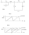
- FIG 1 the basic schematic of a conventional boost converter is sketched. This shows an inductor L1 coupled to an input and in series with a resistor R1 used to measure the inductor current. One side of the inductor is coupled to ground via switch SW1. The same side is also coupled to an output via switch SW2. The output is coupled to ground via a capacitor C1. The switches are controlled by a controller (not shown).
- SW1 In a magnetization phase, SW1 is closed (and SW2 is open). The inductor current increases to a maximum current shown by threshold1. In the demagnetization phase, SW2 is closed (SW1 is open). The energy in the inductor is transferred to the capacitor. In this phase the inductor current decreases.
- the inductor current waveform in DCM is sketched for the maximum current pulse frequency: the new current pulse 'a' is started just after the current through the inductor has reached zero.
- the controller will initiate a new current pulse if its output voltage drops below a certain threshold, related to the intended output voltage.
- a new current pulse is initiated only after the converter's inductor current has dropped to zero.
- the frequency of occurrence of the current pulses is dependent on the required load current of the DC to DC converter.
- the maximum current that can be delivered is limited to the case where a new current pulse is initiated immediately after the inductor current reached zero.
- the switch control circuit used by the embodiments of the invention can work in very much in the same way, however it can also allow new current pulses to be initiated, when the inductor current has dropped below a certain positive, non zero current threshold level. Because a new current pulse can be started before the current has reached zero, this results in a higher frequency of occurrence of current pulses, and in a CCM mode. The obtained higher average inductor current increases the amount of current that the DC to DC converter can deliver, while maintaining its intended output voltage.
- the features of the described embodiments can make it possible to design dc-dc converters with a smaller or minimum of die-area and with small external components.
- the embodiments are based on controlling the time at which a new DCM current pulse is created, by monitoring not only the output voltage of the converter, but also the instantaneous inductor current. They can be used in many kinds of DC-DC converters, including buck, boost, types and so on.
- the embodiments can use a minimum of analog circuitry, and does not need a finite state machine controller to control the switch between DCM and CCM operation. Therefore the required die area and power consumption can be reduced, and hence costs reduced.
- a converter using these features makes it possible to use smaller and cheaper components, because it can work at lower maximum current inductor for a given output current.
- At least some embodiments can work without any circuits for prevention of subharmonic oscillation. Thus complexity, die area and power consumption are reduced. In the following, the working of an example is explained for the case of a boost converter.
- the inductor current waveform of the proposed converter is sketched.
- the new current pulse can start at any time larger than, or equal to time 'ta'.
- 'ta' is determined by the moment at which the inductor current drops below 'threshold2'.
- FIG. 4 shows a schematic view of apparatus according to a first embodiment. This shows some features as already shown in figure 1 .
- a diode D1 is shown in place of switch SW2.
- Switch control circuitry is provided in the form of three comparators coupled to three reference signals to provide thresholds, an AND gate and a flipflop. The output of the flipflop drives the switch SW1.
- a set input of the flipflop is driven by an output of the AND gate.
- the inputs of the AND gate are driven by first and second comparators.
- the first comparator has inputs fed by a measure of the inductor current, and an intermediate threshold (threshold2), and indicates when the inductor current drops below the intermediate threshold.
- the second comparator has inputs fed by a measure of output voltage and a threshold Vout_set, indicating a desired voltage, arranged so that the comparator indicates when the output voltage goes below the set voltage.
- the reset input of the flipflop is fed by a third comparator which has inputs fed by the measure of inductor current and a threshold (threshold1) indicating a maximum inductor current.
- a threshold indicating a maximum inductor current.
- These inductor current thresholds can be fixed or variable thresholds. If variable, there would be circuitry such as an analog multiplier circuit or digital arithmetic circuitry or processor circuitry to provide a threshold which varies with for example input or output voltage or with time.
- Asynchronous magnetization is started in this case as soon as Vout drops below Vout_set. In figure 3 this can result in curve a or b.
- curve a the output voltage has dropped below the set voltage before the inductor current has dropped to the intermediate value, as might happen under a heavy load or rapid increase of load on the output.
- curve b the output voltage has dropped below the set voltage after the inductor current has dropped to the intermediate value, as might happen under a medium load or increase of load.
- curve c the output voltage has dropped below the set voltage after the inductor current has dropped to zero, as might happen under a light load or a decrease of load.
- the proposed type of converter is a true combination of the advantages of the CCM and the DCM type of converter. It can provide in particular embodiments:
- Simple control circuit small area, less design effort
- low power consumption small ratio of peak current to average inductor current (wide choice of inductor and switching elements: small size/ low cost)
- fast transient response constant power efficiency over large range
- stable operation no subharmonic oscillation
- the proposed converter as shown in figure 4 is well suited for applications that need to operate predominantly at small load currents, but occasionally at high load currents.
- the basis of the modified dc-dc converter is the DCM controller.
- the embodiments described help to reduce or remove the need for a high inductor peak current, even for high load currents.
- High load currents can be delivered by seamlessly going over to special form of CCM in case of high load currents. This can be done in some cases with minimum of analog circuitry, and without a digital controller (state-machine). Because of the way in which CCM is realized, it does not require subharmonic oscillation cancellation circuits, and it preserves the fast transient response of the DCM mode. This follows from the non-clocked nature of the resulting CCM modus. (subharmonic oscillation can only arise in clocked converters with an asynchronous element, e.g. the magnetization starts at a clocked moment and the transition from magnetization to demagnetization is asynchronous).
Landscapes
- Engineering & Computer Science (AREA)
- Power Engineering (AREA)
- Dc-Dc Converters (AREA)
Claims (14)
- Convertisseur CC - CC à commutation ayant un composant inductif (L1), un circuit de commande de commutation, et un commutateur (SW1) pouvant être commandé par le circuit de commande de commutation pour amener le convertisseur CC - CC à alterner entre une phase de magnétisation dans laquelle un courant d'induction dans le composant inductif augmente, et une phase de démagnétisation dans laquelle le courant d'induction diminue, le circuit de commande de commutation ayant un premier comparateur pour comparer un courant d'induction à un seuil intermédiaire (Ifract) au-dessous d'un courant d'induction maximal (Ipk), et un deuxième comparateur pour comparer une tension de sortie (Vout) à un seuil de tension (vout_set), caractérisé en ce que le seuil intermédiaire est un niveau de courant de seuil non nul, positif, et en ce que les sorties des premier et deuxième comparateurs sont couplées pour amener le commutateur à commuter de la phase de démagnétisation à la phase de magnétisation lorsque le deuxième comparateur indique que la tension de sortie chute au-dessous du seuil de tension si le premier comparateur indique déjà que le courant d'induction a chuté au-dessous du seuil intermédiaire, ou lorsque le premier comparateur indique que le courant d'induction chute au-dessous du seuil intermédiaire, et si le deuxième comparateur indique déjà que la tension de sortie a chuté au-dessous du seuil de tension.
- Convertisseur selon la revendication 1, le circuit de commande de commutation ayant un troisième comparateur agencé pour comparer le courant d'induction à un seuil de courant maximal (Ipk) et couplé pour amener le commutateur à commuter de la phase de magnétisation à la phase de démagnétisation lorsque le troisième comparateur indique que le courant d'induction est monté jusqu'au seuil de courant maximal.
- Convertisseur selon la revendication 1 ou 2, le circuit de commande de commutation ayant un composant à bascule bistable couplé au commutateur pour maintenir l'état du commutateur jusqu'à ce que des entrées de mise à un ou de remise à zéro de la bascule bistable soient activées par les comparateurs.
- Convertisseur selon l'une quelconque des revendications précédentes, le circuit de commande de commutation ayant des circuits pour faire varier le seuil intermédiaire.
- Convertisseur selon l'une quelconque des revendications précédentes, le circuit de commande de commutation ayant des circuits pour faire varier le seuil de courant maximal.
- Convertisseur selon l'une quelconque des revendications précédentes, n'ayant pas de circuits pour empêcher une oscillation sous-harmonique.
- Convertisseur selon l'une quelconque des revendications précédentes n'ayant pas de circuits pour mettre en oeuvre un automate fini pour la commande de la commutation.
- Circuit intégré ayant le convertisseur selon l'une quelconque des revendications précédentes.
- Procédé de commande d'un convertisseur CC - CC à commutation ayant un composant inductif (L1), et un commutateur (SW1) pour amener le convertisseur CC - CC à alterner entre une phase de magnétisation dans laquelle un courant d'induction dans le composant inductif augmente, et une phase de démagnétisation dans laquelle le courant d'induction diminue, le procédé ayant les étapes d'une première comparaison d'un courant d'induction à un seuil intermédiaire, (Ifract) au-dessous d'un courant d'induction maximal, d'une deuxième comparaison d'une tension de sortie à un seuil de tension (vout_set), caractérisé en ce que le seuil intermédiaire est un niveau de seuil de courant non nul, positif, et en ce que le procédé comprend l'étape d'utilisation de résultats des première et deuxième comparaisons pour amener le commutateur à commuter de la phase de démagnétisation à la phase de magnétisation lorsque la deuxième comparaison indique que la tension de sortie chute au-dessous du seuil de tension si la première comparaison indique déjà que le courant d'induction a chuté au-dessous du seuil intermédiaire, ou lorsque la première comparaison indique que le courant d'induction a chuté au-dessous du seuil intermédiaire, si la deuxième comparaison indique déjà que la tension de sortie a chuté au-dessous du seuil de tension.
- Procédé selon la revendication 9 ayant l'étape de réalisation d'une troisième comparaison, comparant le courant d'induction à un seuil de courant maximal et amenant le commutateur à commuter de la phase de magnétisation à la phase de démagnétisation lorsque la troisième comparaison indique que le courant d'induction est monté jusqu'au seuil ce courant maximal.
- Procédé selon la revendication 9 cu 10 ayant l'étape de faire varier le seuil intermédiaire.
- Procédé selon l'une quelconque des revendications précédentes 9, 10 ou 11, ayant l'étape de faire varier le seuil de courant maximal.
- Procédé selon l'une quelconque des revendications 9 à 12, comprenant en outre la prévention d'oscillation sous-harmonique.
- Procédé selon l'une quelconque des revendications 9 à 13, comprenant en outre le maintien de l'état du commutateur jusqu'à la mise à un ou la remise à zéro selon les sorties des première et deuxième comparaisons.
Priority Applications (3)
| Application Number | Priority Date | Filing Date | Title |
|---|---|---|---|
| AT09160037T ATE552645T1 (de) | 2009-05-12 | 2009-05-12 | Gleichstromwandler mit diskontinuierlichen und kontinuierlichen leitmodi |
| EP09160037A EP2251966B1 (fr) | 2009-05-12 | 2009-05-12 | Convertisseur CC-CC avec modes de conduction discontinue et continue |
| PCT/EP2010/052509 WO2010130473A1 (fr) | 2009-05-12 | 2010-02-26 | Convertisseur continu - continu doté de modes de conduction continus et discontinus |
Applications Claiming Priority (1)
| Application Number | Priority Date | Filing Date | Title |
|---|---|---|---|
| EP09160037A EP2251966B1 (fr) | 2009-05-12 | 2009-05-12 | Convertisseur CC-CC avec modes de conduction discontinue et continue |
Publications (2)
| Publication Number | Publication Date |
|---|---|
| EP2251966A1 EP2251966A1 (fr) | 2010-11-17 |
| EP2251966B1 true EP2251966B1 (fr) | 2012-04-04 |
Family
ID=40941678
Family Applications (1)
| Application Number | Title | Priority Date | Filing Date |
|---|---|---|---|
| EP09160037A Not-in-force EP2251966B1 (fr) | 2009-05-12 | 2009-05-12 | Convertisseur CC-CC avec modes de conduction discontinue et continue |
Country Status (3)
| Country | Link |
|---|---|
| EP (1) | EP2251966B1 (fr) |
| AT (1) | ATE552645T1 (fr) |
| WO (1) | WO2010130473A1 (fr) |
Families Citing this family (6)
| Publication number | Priority date | Publication date | Assignee | Title |
|---|---|---|---|---|
| EP2704301B1 (fr) | 2012-08-31 | 2016-07-27 | Stichting IMEC Nederland | Convertisseur CC-CC et son procédé de commande |
| CN105450028A (zh) * | 2014-06-18 | 2016-03-30 | 台达电子企业管理(上海)有限公司 | 变换器及其控制方法 |
| JP6479372B2 (ja) * | 2014-09-02 | 2019-03-06 | 日立オートモティブシステムズ株式会社 | 電源装置 |
| EP3474407B1 (fr) | 2017-10-18 | 2020-01-15 | e-peas S.A. | Circuit intégré de gestion de puissance pour la récupération d'énergie comportant une sélection de puissance multi-mode |
| JP2021158712A (ja) * | 2020-03-25 | 2021-10-07 | Tdk株式会社 | スイッチング電源装置およびスイッチング電源システム |
| US11563379B2 (en) | 2021-05-03 | 2023-01-24 | Advanced Energy Industries, Inc. | Phase current balancing for multiphase coupled inductor converter |
Family Cites Families (5)
| Publication number | Priority date | Publication date | Assignee | Title |
|---|---|---|---|---|
| US5801518A (en) | 1995-02-28 | 1998-09-01 | Seiko Instruments Inc. | Pulse frequency modulated DC-DC converter |
| US6396252B1 (en) | 2000-12-14 | 2002-05-28 | National Semiconductor Corporation | Switching DC-to-DC converter with discontinuous pulse skipping and continuous operating modes without external sense resistor |
| US6556462B1 (en) | 2002-06-28 | 2003-04-29 | General Electric Company | High power factor converter with a boost circuit having continuous/discontinuous modes |
| US6972548B2 (en) | 2003-11-25 | 2005-12-06 | Aimtron Technology Corp. | Pulse frequency modulated voltage regulator capable of prolonging a minimum off-time |
| US7266001B1 (en) * | 2004-03-19 | 2007-09-04 | Marvell International Ltd. | Method and apparatus for controlling power factor correction |
-
2009
- 2009-05-12 AT AT09160037T patent/ATE552645T1/de active
- 2009-05-12 EP EP09160037A patent/EP2251966B1/fr not_active Not-in-force
-
2010
- 2010-02-26 WO PCT/EP2010/052509 patent/WO2010130473A1/fr not_active Ceased
Also Published As
| Publication number | Publication date |
|---|---|
| WO2010130473A1 (fr) | 2010-11-18 |
| EP2251966A1 (fr) | 2010-11-17 |
| ATE552645T1 (de) | 2012-04-15 |
Similar Documents
| Publication | Publication Date | Title |
|---|---|---|
| US8519691B2 (en) | Current limiting for DC-DC converters | |
| CN101785173B (zh) | 使用动态负载检测和跟踪来提高功率转换效率 | |
| CN111327201B (zh) | 具有限制控制装置以控制开关周期或开关频率的变化速率的功率转换器 | |
| US7872458B2 (en) | DC-to-DC converter | |
| US8049481B2 (en) | Adaptive multi-mode digital control improving light-load efficiency in switching power converters | |
| EP1926199B1 (fr) | Convertisseur abaisseur avec pré-excitation de l'inductance | |
| JP4678215B2 (ja) | スイッチング電源装置 | |
| TWI581547B (zh) | 用於限制轉換器之電流的裝置、調變器和方法 | |
| US10148176B2 (en) | DC to DC converter with pulse width modulation and a clamping circuit for non-pulse width modulation control | |
| US9825524B2 (en) | Dynamic control loop for switching regulators | |
| KR101851930B1 (ko) | 교류-직류 컨버터 | |
| US9520785B2 (en) | Nonlinear control loop for DC-DC converters | |
| EP2251966B1 (fr) | Convertisseur CC-CC avec modes de conduction discontinue et continue | |
| US9160238B2 (en) | Power converter with current feedback loop | |
| US20110001460A1 (en) | Lower power controller for dc to dc converters | |
| US11362579B2 (en) | Peak voltage overshoot control for switch mode power converters | |
| CN104377949B (zh) | 开关整流器启动控制方法及其装置 | |
| CN109936277A (zh) | 转换器及其驱动及控制方法 | |
| JP5495252B2 (ja) | 電源装置 | |
| JP3416219B2 (ja) | 電源装置 | |
| JP2005287249A (ja) | スイッチング電源装置 | |
| KR20170050014A (ko) | 역률 보상 장치 및 이의 동작 방법 | |
| EP1372253A1 (fr) | Appareil et procédé pour la réduction de la sollicitation de tension dans un circuit de correction du facteur de puissance à étage unique et avec un commutateur unique. | |
| KR20200078110A (ko) | 양극성 펄스 전원 공급 장치 | |
| JPH09121534A (ja) | Dc/dcコンバータ |
Legal Events
| Date | Code | Title | Description |
|---|---|---|---|
| PUAI | Public reference made under article 153(3) epc to a published international application that has entered the european phase |
Free format text: ORIGINAL CODE: 0009012 |
|
| AK | Designated contracting states |
Kind code of ref document: A1 Designated state(s): AT BE BG CH CY CZ DE DK EE ES FI FR GB GR HR HU IE IS IT LI LT LU LV MC MK MT NL NO PL PT RO SE SI SK TR |
|
| 17P | Request for examination filed |
Effective date: 20110517 |
|
| GRAP | Despatch of communication of intention to grant a patent |
Free format text: ORIGINAL CODE: EPIDOSNIGR1 |
|
| GRAS | Grant fee paid |
Free format text: ORIGINAL CODE: EPIDOSNIGR3 |
|
| GRAA | (expected) grant |
Free format text: ORIGINAL CODE: 0009210 |
|
| AK | Designated contracting states |
Kind code of ref document: B1 Designated state(s): AT BE BG CH CY CZ DE DK EE ES FI FR GB GR HR HU IE IS IT LI LT LU LV MC MK MT NL NO PL PT RO SE SI SK TR |
|
| REG | Reference to a national code |
Ref country code: GB Ref legal event code: FG4D |
|
| REG | Reference to a national code |
Ref country code: CH Ref legal event code: EP |
|
| REG | Reference to a national code |
Ref country code: AT Ref legal event code: REF Ref document number: 552645 Country of ref document: AT Kind code of ref document: T Effective date: 20120415 |
|
| REG | Reference to a national code |
Ref country code: IE Ref legal event code: FG4D |
|
| REG | Reference to a national code |
Ref country code: DE Ref legal event code: R096 Ref document number: 602009006220 Country of ref document: DE Effective date: 20120531 |
|
| REG | Reference to a national code |
Ref country code: NL Ref legal event code: VDEP Effective date: 20120404 |
|
| REG | Reference to a national code |
Ref country code: AT Ref legal event code: MK05 Ref document number: 552645 Country of ref document: AT Kind code of ref document: T Effective date: 20120404 |
|
| LTIE | Lt: invalidation of european patent or patent extension |
Effective date: 20120404 |
|
| PG25 | Lapsed in a contracting state [announced via postgrant information from national office to epo] |
Ref country code: IS Free format text: LAPSE BECAUSE OF FAILURE TO SUBMIT A TRANSLATION OF THE DESCRIPTION OR TO PAY THE FEE WITHIN THE PRESCRIBED TIME-LIMIT Effective date: 20120804 Ref country code: LT Free format text: LAPSE BECAUSE OF FAILURE TO SUBMIT A TRANSLATION OF THE DESCRIPTION OR TO PAY THE FEE WITHIN THE PRESCRIBED TIME-LIMIT Effective date: 20120404 Ref country code: PL Free format text: LAPSE BECAUSE OF FAILURE TO SUBMIT A TRANSLATION OF THE DESCRIPTION OR TO PAY THE FEE WITHIN THE PRESCRIBED TIME-LIMIT Effective date: 20120404 Ref country code: SE Free format text: LAPSE BECAUSE OF FAILURE TO SUBMIT A TRANSLATION OF THE DESCRIPTION OR TO PAY THE FEE WITHIN THE PRESCRIBED TIME-LIMIT Effective date: 20120404 Ref country code: SI Free format text: LAPSE BECAUSE OF FAILURE TO SUBMIT A TRANSLATION OF THE DESCRIPTION OR TO PAY THE FEE WITHIN THE PRESCRIBED TIME-LIMIT Effective date: 20120404 Ref country code: NO Free format text: LAPSE BECAUSE OF FAILURE TO SUBMIT A TRANSLATION OF THE DESCRIPTION OR TO PAY THE FEE WITHIN THE PRESCRIBED TIME-LIMIT Effective date: 20120704 Ref country code: FI Free format text: LAPSE BECAUSE OF FAILURE TO SUBMIT A TRANSLATION OF THE DESCRIPTION OR TO PAY THE FEE WITHIN THE PRESCRIBED TIME-LIMIT Effective date: 20120404 Ref country code: CY Free format text: LAPSE BECAUSE OF FAILURE TO SUBMIT A TRANSLATION OF THE DESCRIPTION OR TO PAY THE FEE WITHIN THE PRESCRIBED TIME-LIMIT Effective date: 20120404 |
|
| PG25 | Lapsed in a contracting state [announced via postgrant information from national office to epo] |
Ref country code: GR Free format text: LAPSE BECAUSE OF FAILURE TO SUBMIT A TRANSLATION OF THE DESCRIPTION OR TO PAY THE FEE WITHIN THE PRESCRIBED TIME-LIMIT Effective date: 20120705 Ref country code: LV Free format text: LAPSE BECAUSE OF FAILURE TO SUBMIT A TRANSLATION OF THE DESCRIPTION OR TO PAY THE FEE WITHIN THE PRESCRIBED TIME-LIMIT Effective date: 20120404 Ref country code: HR Free format text: LAPSE BECAUSE OF FAILURE TO SUBMIT A TRANSLATION OF THE DESCRIPTION OR TO PAY THE FEE WITHIN THE PRESCRIBED TIME-LIMIT Effective date: 20120404 Ref country code: PT Free format text: LAPSE BECAUSE OF FAILURE TO SUBMIT A TRANSLATION OF THE DESCRIPTION OR TO PAY THE FEE WITHIN THE PRESCRIBED TIME-LIMIT Effective date: 20120806 |
|
| PG25 | Lapsed in a contracting state [announced via postgrant information from national office to epo] |
Ref country code: MC Free format text: LAPSE BECAUSE OF NON-PAYMENT OF DUE FEES Effective date: 20120531 Ref country code: BE Free format text: LAPSE BECAUSE OF FAILURE TO SUBMIT A TRANSLATION OF THE DESCRIPTION OR TO PAY THE FEE WITHIN THE PRESCRIBED TIME-LIMIT Effective date: 20120404 |
|
| PG25 | Lapsed in a contracting state [announced via postgrant information from national office to epo] |
Ref country code: NL Free format text: LAPSE BECAUSE OF FAILURE TO SUBMIT A TRANSLATION OF THE DESCRIPTION OR TO PAY THE FEE WITHIN THE PRESCRIBED TIME-LIMIT Effective date: 20120404 Ref country code: EE Free format text: LAPSE BECAUSE OF FAILURE TO SUBMIT A TRANSLATION OF THE DESCRIPTION OR TO PAY THE FEE WITHIN THE PRESCRIBED TIME-LIMIT Effective date: 20120404 Ref country code: AT Free format text: LAPSE BECAUSE OF FAILURE TO SUBMIT A TRANSLATION OF THE DESCRIPTION OR TO PAY THE FEE WITHIN THE PRESCRIBED TIME-LIMIT Effective date: 20120404 Ref country code: RO Free format text: LAPSE BECAUSE OF FAILURE TO SUBMIT A TRANSLATION OF THE DESCRIPTION OR TO PAY THE FEE WITHIN THE PRESCRIBED TIME-LIMIT Effective date: 20120404 Ref country code: CZ Free format text: LAPSE BECAUSE OF FAILURE TO SUBMIT A TRANSLATION OF THE DESCRIPTION OR TO PAY THE FEE WITHIN THE PRESCRIBED TIME-LIMIT Effective date: 20120404 Ref country code: DK Free format text: LAPSE BECAUSE OF FAILURE TO SUBMIT A TRANSLATION OF THE DESCRIPTION OR TO PAY THE FEE WITHIN THE PRESCRIBED TIME-LIMIT Effective date: 20120404 Ref country code: SK Free format text: LAPSE BECAUSE OF FAILURE TO SUBMIT A TRANSLATION OF THE DESCRIPTION OR TO PAY THE FEE WITHIN THE PRESCRIBED TIME-LIMIT Effective date: 20120404 |
|
| PLBE | No opposition filed within time limit |
Free format text: ORIGINAL CODE: 0009261 |
|
| STAA | Information on the status of an ep patent application or granted ep patent |
Free format text: STATUS: NO OPPOSITION FILED WITHIN TIME LIMIT |
|
| REG | Reference to a national code |
Ref country code: IE Ref legal event code: MM4A |
|
| PG25 | Lapsed in a contracting state [announced via postgrant information from national office to epo] |
Ref country code: IT Free format text: LAPSE BECAUSE OF FAILURE TO SUBMIT A TRANSLATION OF THE DESCRIPTION OR TO PAY THE FEE WITHIN THE PRESCRIBED TIME-LIMIT Effective date: 20120404 Ref country code: MK Free format text: LAPSE BECAUSE OF FAILURE TO SUBMIT A TRANSLATION OF THE DESCRIPTION OR TO PAY THE FEE WITHIN THE PRESCRIBED TIME-LIMIT Effective date: 20120404 |
|
| REG | Reference to a national code |
Ref country code: FR Ref legal event code: ST Effective date: 20130131 |
|
| 26N | No opposition filed |
Effective date: 20130107 |
|
| REG | Reference to a national code |
Ref country code: DE Ref legal event code: R119 Ref document number: 602009006220 Country of ref document: DE Effective date: 20121201 |
|
| PG25 | Lapsed in a contracting state [announced via postgrant information from national office to epo] |
Ref country code: IE Free format text: LAPSE BECAUSE OF NON-PAYMENT OF DUE FEES Effective date: 20120512 Ref country code: FR Free format text: LAPSE BECAUSE OF NON-PAYMENT OF DUE FEES Effective date: 20120604 Ref country code: ES Free format text: LAPSE BECAUSE OF FAILURE TO SUBMIT A TRANSLATION OF THE DESCRIPTION OR TO PAY THE FEE WITHIN THE PRESCRIBED TIME-LIMIT Effective date: 20120715 |
|
| PG25 | Lapsed in a contracting state [announced via postgrant information from national office to epo] |
Ref country code: DE Free format text: LAPSE BECAUSE OF NON-PAYMENT OF DUE FEES Effective date: 20121201 |
|
| PG25 | Lapsed in a contracting state [announced via postgrant information from national office to epo] |
Ref country code: BG Free format text: LAPSE BECAUSE OF FAILURE TO SUBMIT A TRANSLATION OF THE DESCRIPTION OR TO PAY THE FEE WITHIN THE PRESCRIBED TIME-LIMIT Effective date: 20120704 Ref country code: MT Free format text: LAPSE BECAUSE OF FAILURE TO SUBMIT A TRANSLATION OF THE DESCRIPTION OR TO PAY THE FEE WITHIN THE PRESCRIBED TIME-LIMIT Effective date: 20120404 |
|
| REG | Reference to a national code |
Ref country code: CH Ref legal event code: PL |
|
| PG25 | Lapsed in a contracting state [announced via postgrant information from national office to epo] |
Ref country code: LI Free format text: LAPSE BECAUSE OF NON-PAYMENT OF DUE FEES Effective date: 20130531 Ref country code: CH Free format text: LAPSE BECAUSE OF NON-PAYMENT OF DUE FEES Effective date: 20130531 |
|
| PG25 | Lapsed in a contracting state [announced via postgrant information from national office to epo] |
Ref country code: TR Free format text: LAPSE BECAUSE OF FAILURE TO SUBMIT A TRANSLATION OF THE DESCRIPTION OR TO PAY THE FEE WITHIN THE PRESCRIBED TIME-LIMIT Effective date: 20120404 |
|
| PG25 | Lapsed in a contracting state [announced via postgrant information from national office to epo] |
Ref country code: LU Free format text: LAPSE BECAUSE OF NON-PAYMENT OF DUE FEES Effective date: 20120512 |
|
| PG25 | Lapsed in a contracting state [announced via postgrant information from national office to epo] |
Ref country code: HU Free format text: LAPSE BECAUSE OF FAILURE TO SUBMIT A TRANSLATION OF THE DESCRIPTION OR TO PAY THE FEE WITHIN THE PRESCRIBED TIME-LIMIT Effective date: 20090512 |
|
| PGFP | Annual fee paid to national office [announced via postgrant information from national office to epo] |
Ref country code: GB Payment date: 20170426 Year of fee payment: 9 |
|
| GBPC | Gb: european patent ceased through non-payment of renewal fee |
Effective date: 20180512 |
|
| PG25 | Lapsed in a contracting state [announced via postgrant information from national office to epo] |
Ref country code: GB Free format text: LAPSE BECAUSE OF NON-PAYMENT OF DUE FEES Effective date: 20180512 |