EP2253045B1 - Boîtiers de circuit intégré (ci) à radiofréquence (rf) dotés d antennes de connexion à ouverture couplée intégrée(s) - Google Patents
Boîtiers de circuit intégré (ci) à radiofréquence (rf) dotés d antennes de connexion à ouverture couplée intégrée(s) Download PDFInfo
- Publication number
- EP2253045B1 EP2253045B1 EP08872709.4A EP08872709A EP2253045B1 EP 2253045 B1 EP2253045 B1 EP 2253045B1 EP 08872709 A EP08872709 A EP 08872709A EP 2253045 B1 EP2253045 B1 EP 2253045B1
- Authority
- EP
- European Patent Office
- Prior art keywords
- package
- patch
- feed line
- ground plane
- substrate layer
- Prior art date
- Legal status (The legal status is an assumption and is not a legal conclusion. Google has not performed a legal analysis and makes no representation as to the accuracy of the status listed.)
- Active
Links
Images




Classifications
-
- H—ELECTRICITY
- H01—ELECTRIC ELEMENTS
- H01Q—ANTENNAS, i.e. RADIO AERIALS
- H01Q23/00—Antennas with active circuits or circuit elements integrated within them or attached to them
-
- H—ELECTRICITY
- H01—ELECTRIC ELEMENTS
- H01Q—ANTENNAS, i.e. RADIO AERIALS
- H01Q1/00—Details of, or arrangements associated with, antennas
- H01Q1/12—Supports; Mounting means
- H01Q1/22—Supports; Mounting means by structural association with other equipment or articles
- H01Q1/2283—Supports; Mounting means by structural association with other equipment or articles mounted in or on the surface of a semiconductor substrate as a chip-type antenna or integrated with other components into an IC package
-
- H—ELECTRICITY
- H01—ELECTRIC ELEMENTS
- H01Q—ANTENNAS, i.e. RADIO AERIALS
- H01Q1/00—Details of, or arrangements associated with, antennas
- H01Q1/36—Structural form of radiating elements, e.g. cone, spiral, umbrella; Particular materials used therewith
- H01Q1/38—Structural form of radiating elements, e.g. cone, spiral, umbrella; Particular materials used therewith formed by a conductive layer on an insulating support
-
- H—ELECTRICITY
- H01—ELECTRIC ELEMENTS
- H01Q—ANTENNAS, i.e. RADIO AERIALS
- H01Q9/00—Electrically-short antennas having dimensions not more than twice the operating wavelength and consisting of conductive active radiating elements
- H01Q9/04—Resonant antennas
- H01Q9/0407—Substantially flat resonant element parallel to ground plane, e.g. patch antenna
- H01Q9/045—Substantially flat resonant element parallel to ground plane, e.g. patch antenna with particular feeding means
- H01Q9/0457—Substantially flat resonant element parallel to ground plane, e.g. patch antenna with particular feeding means electromagnetically coupled to the feed line
-
- H—ELECTRICITY
- H10—SEMICONDUCTOR DEVICES; ELECTRIC SOLID-STATE DEVICES NOT OTHERWISE PROVIDED FOR
- H10W—GENERIC PACKAGES, INTERCONNECTIONS, CONNECTORS OR OTHER CONSTRUCTIONAL DETAILS OF DEVICES COVERED BY CLASS H10
- H10W44/00—Electrical arrangements for controlling or matching impedance
- H10W44/20—Electrical arrangements for controlling or matching impedance at high-frequency [HF] or radio frequency [RF]
-
- H—ELECTRICITY
- H10—SEMICONDUCTOR DEVICES; ELECTRIC SOLID-STATE DEVICES NOT OTHERWISE PROVIDED FOR
- H10W—GENERIC PACKAGES, INTERCONNECTIONS, CONNECTORS OR OTHER CONSTRUCTIONAL DETAILS OF DEVICES COVERED BY CLASS H10
- H10W44/00—Electrical arrangements for controlling or matching impedance
- H10W44/20—Electrical arrangements for controlling or matching impedance at high-frequency [HF] or radio frequency [RF]
- H10W44/241—Electrical arrangements for controlling or matching impedance at high-frequency [HF] or radio frequency [RF] for passive devices or passive elements
- H10W44/248—Electrical arrangements for controlling or matching impedance at high-frequency [HF] or radio frequency [RF] for passive devices or passive elements for antennas
-
- H—ELECTRICITY
- H10—SEMICONDUCTOR DEVICES; ELECTRIC SOLID-STATE DEVICES NOT OTHERWISE PROVIDED FOR
- H10W—GENERIC PACKAGES, INTERCONNECTIONS, CONNECTORS OR OTHER CONSTRUCTIONAL DETAILS OF DEVICES COVERED BY CLASS H10
- H10W90/00—Package configurations
- H10W90/701—Package configurations characterised by the relative positions of pads or connectors relative to package parts
- H10W90/721—Package configurations characterised by the relative positions of pads or connectors relative to package parts of bump connectors
- H10W90/724—Package configurations characterised by the relative positions of pads or connectors relative to package parts of bump connectors between a chip and a stacked insulating package substrate, interposer or RDL
Definitions
- the present invention generally relates to communications circuitry, and, more particularly, to radio frequency (RF) integrated circuit (IC) packages.
- RF radio frequency
- a wireless network In a wireless network, the connectivity and communication between devices is achieved through antennas attached to receivers or transmitters, in order to radiate the desired signals to or from other elements of the network.
- radio communication systems such as millimeter-wave radios
- discrete components are usually assembled with low integration levels. These systems are often assembled using expensive and bulky waveguides and package-level or board-level microstrip structures to interconnect semiconductors and their required transmitter- or receiver-antennas.
- semiconductor technology and packaging engineering With recent progress in semiconductor technology and packaging engineering, the dimensions of these radio communication systems have become smaller. For applications such as wireless universal serial bus (USB), the operating distance is limited to about a meter; and a single antenna with about 7 dBi at 60 GHz will provide the necessary antenna gain.
- USB wireless universal serial bus
- antenna gains as high as 30 dBi, depending on the application, are required.
- high gain antennas for wireless video applications have very narrow beam widths, so pointing the antenna is very difficult for consumers. Therefore, a radiation pattern steerable array (also a phased array) is necessary.
- Phased arrays are also widely used in military radars. However, packaging RF chips with integrated antennas or phased arrays is extremely difficult and very expensive due to the expensive components and extensive labor involved.
- US patent application US 2007/0026567 A1 in the name of Beer, Gottfried et al. discloses a semiconductor module having components for microwave engineering in a plastic casing.
- the semiconductor module is described as having a principal surface with an upper side of a plastic package moulding compound and at least one active upper side of a semiconductor chip.
- Disposed on the principal surface is a multilayered conductor track structure which alternately comprises structured metal layers and structured insulation layers, where at least one of the insulation layers and/or the plastic package moulding compound has at least one microwave insulation region.
- Principles of the present invention provide techniques for implementing RF IC packages with integrated aperture-coupled patch antennas.
- the present invention provides a radio-frequency integrated circuit chip package with at least one integrated aperture-coupled patch antenna.
- the package comprises at least one planar patch formed in a first metal layer; at least one planar ground plane formed in a second metal layer spaced inwardly from said planar patch and parallel thereto.
- the ground plane is formed with at least one coupling aperture slot therein, said slot being opposed to said patch.
- At least one feed line is formed in a third metal layer spaced inwardly from said ground plane and parallel thereto.
- At least one radio frequency chip is spaced inwardly from said feed line and coupled to said feed line and said ground plane.
- a first substrate layer is spaced inwardly from said feed line, said first substrate layer being formed with a chip-receiving cavity, said chip being located in said chip-receiving cavity.
- a second substrate layer is interposed between said ground plane and a plane defined by said patch.
- An additional substrate layer is located outwardly from said planar patch, wherein said patch is formed on an inner surface of said additional substrate layer.
- a third substrate layer is interposed between said ground plane and said feed line.
- a reflector spaced inwardly from said feed line, by said first substrate layer and opposed to said coupling aperture slot.
- An air cavity is formed in said second substrate layer, said air cavity being located between said patch and said coupling aperture slot in said ground plane, wherein said at least one planar patch is located in said air cavity.
- a vent hole is formed in said secondsubstrate layer or said additional substrate in communication with said air cavity.
- One or more embodiments of the invention provide an apparatus and method for low cost packages with integrated antennas and phased arrays operating in the millimeter wave (mmWave) range.
- An exemplary inventive package with integrated antennas is based on a multilayer printed circuit board (PCB).
- the package contains multiple cavities for implementing high performance antenna(s) or antenna arrays and housing mmWave radio frequency (RF) integrated circuit chips.
- RF radio frequency
- One or more embodiments of the invention also provide techniques to overcome the difficulties in making internal cavities and to avoid the need to employ wire bond technology at mmWave frequencies.
- Embodiments of the inventive packaging technology are consistent with the PCB manufacturing process and can be used for packages with an integrated antenna or antenna array.
- Instances of the invention thus provide low cost packaging with integrated antennas or planar phased arrays; in particular, chip packaging with integrated antennas or planar phased array designs for mmWave frequencies and above.
- Typical chip packages with integrated antennas have three major parts: (i) an RF chip, (ii) one or more antennas, and (iii) a package carrier (and in some instances, a package lid or cover, or an encapsulant to protect the package).
- a package carrier and in some instances, a package lid or cover, or an encapsulant to protect the package.
- One or more embodiments of the invention provide a package that has high performance antennas, an interface for flip-chipping an RF chip and an interface for flip-chipping the package to a printed circuit mother board.
- FIG. 1 shows a cross-sectional view of an exemplary package 100, according to an aspect of the invention. Note that section lining is omitted for clarity.
- the package has seven total layers, including substrate and bounding layers. For mmWave applications, especially for frequencies above 60 GHz, bounding film and/or layer thickness has to be considered in the design process. Given the teachings herein, a person having ordinary skill in the antenna and packaging arts will know how to take the thickness into account and how to employ high precision PCB fabrication techniques to make embodiments of the invention.
- the package 100 also has a number of metal layers. In particular, there is an outermost substrate 102. Immediately inward therefrom is a metal layer used for the patch(es) 104 of the patch antenna(s).
- a bound film layer 106 Inward of the substrate 102 and patch antenna 104 (only a single antenna is depicted in FIG. 1 , but more can be provided as discussed below) are a bound film layer 106, another substrate layer 108, and another bound film layer 109. Another metal layer, inward of bound film 109, is used for the ground plane 110 of the patch antenna. Slot(s) 113 on the ground plane are used for the apertures of the aperture-coupled patch antennas. The ground plane 110 also separates the radiating elements (patches) 104 from the feed line(s) and the RF chip(s), discussed below.
- Another substrate 112 is inward from ground plane 110.
- Another metal layer is inward from substrate 112 and is used to implement the antenna feed line(s) 114, pads 116, 118, 120 for RF chip connections (preferably a flip-chip/C4 ("controlled collapse chip connection") type of connection), and interconnection(s) 122 (as appropriate) to one or more vias, such as via 124, in a further bound film layer 126 inward of the metal layer forming feed line 114, and a further substrate 128 inward of bound film 126.
- a still further metal layer provides all the pads for signal, control, power supply, and ground connections to the mother PCB (the mother PCB is omitted from the figure for clarity).
- Pads may include ground pad 130 interconnected with ground plane 110 through ground via 140, as well as one or more of signal, power, and control pads exemplified by pad 132 connected to interconnection 122 and antipad 142 by via 124.
- the vias may be, for example, plated through holes.
- Package pads 134 may also be provided.
- a reflector 144 is also implemented on the same metal layer as the pads 130, 132, 134. In some instances, as discussed below, the reflector 144 is embedded.
- the chip 162 preferably has a plurality of solder dots connected directly to the chip connection pads 116, 118, 120.
- vent hole(s) 152 are employed. These holes can be designed such that they have little effect on the antenna performance.
- hole 152 can be located near the middle of the cavity 150 or close to the edge of the cavity 150, and can be made relatively small, consistent with adequate venting.
- the vent holes can be on the top (outermost part of) the cavity 150 as shown in FIG. 1 or on the side of the cavity as discussed below, depending on the manufacturing process used.
- the ground plane 110 is also used for making ground connections through vias (e.g., via 140) and signal, power, and control connections through vias and antipads (e.g., via 124 with antipad 142, illustrative of a via with antipad that could be used for signal, power, or control functionality).
- vias e.g., via 140
- antipads e.g., via 124 with antipad 142, illustrative of a via with antipad that could be used for signal, power, or control functionality.
- Antipads are beneficial from a manufacturing standpoint, and result in increased reliability, as it is difficult to achieve reliability in partial vias (i.e., vias such as via 124 that do not extend completely through a structure) without use of antipads.
- An open chip-receiving cavity or socket 160 is realized in the substrate 128 and bound film 126. This socket is used to hold the RF chip 162. The chip is attached to the package through flip-chip bonding.
- mmWave components are in the package 100.
- Vias 124, 140 are used to pass through DC or much lower frequency signals.
- the package 100 may advantageously be attached to the mother board (not shown) through a ball grid array (BGA).
- BGA ball grid array
- FIG. 2 shows an embodiment substantially similar to embodiment 100 except that reflector 144 is encapsulated by an additional bound layer 170 inward of reflector 144 and an additional substrate 172 inward of bound layer 170. Similar items have received the same reference number and will not be described again.
- Chip receiving socket 160 is also formed in substrate 172 and bound layer 170 in this embodiment.
- FIG. 3 shows an embodiment substantially similar to embodiment 200 except that vent 352 runs sideways through layer 108 so as to vent cavity 150. Similar items have received the same reference number and will not be described again.
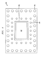
- FIG. 4 presents a bottom view 400 where chip 162 is encapsulated with encapsulant 402.
- the chip can be partially or completely encapsulated, for example, for purposes of resisting humidity.
- a plurality of outer pads 404 may correspond, for example, to attachment, heat conduction, or ground pads such as pad 130, while a plurality of inner pads 406 may correspond, for example, to signal, control, or power pads such as pad 132.
- the reflector is embedded.
- FIG. 5 shows a view 500 similar to view 400 but of a package with a reflector 144, such as in FIG. 1 . Similar items have received the same reference number and will not be described again.
- FIG. 6 shows an exemplary package 600 with a 2x2 planar phased array layout. It is possible to have more than two antennas on each row. This basic 2x2 array can be used to form much larger arrays.
- first antenna patch 104 with first feed line 114 also included are second, third and fourth antenna patches 602, 604, 606 with corresponding second, third and fourth feed lines 608, 610, 612.
- Each feed line is connected to chip 162 as described above.
- the feed lines are shown ending at the patches in FIG. 6 , it will be appreciated that they may overlap same when viewed in top or bottom plan views, and are spaced from the corresponding patch and coupling aperture when viewed in cross-section as shown in FIGS. 1-3 .
- aspects of the invention include a package with a socket for an RF chip, and a planar antenna.
- the RF chip is flip-chip attached to the package.
- Internal cavities are used to improve the patch bandwidth. Venting holes are used to remove the hot gases during the PCB manufacturing process.
- the package can be attached to the mother PCB through a BGA.
- the package can implement a planar phased array.
- radio-frequency integrated circuit chip package according to the invention is defined by independent claim 1.
- Optional features are set ou in the dependent claims.
- Non-limiting examples of materials that may be used include thermoset plastic/ceramic/woven glass or similar laminates such as the Rogers RO4000 ® series of materials (and other compatible materials) available from Rogers Corporation of Rogers, Connecticut USA, as well as copper for metal layers, possibly gold-plated on pads or other exposed areas.
- embodiments of the invention such as 100, 200, and 300, provide a complete package and not a mere patch antenna separate from the chip and other packaging.
- vias such as 124, 140 may be formed, for example, using plated through holes.
- the second substrate layer such as that formed by substrate 108 and bound films 106, 109, is interposed in a region between the ground plane 110 and a plane defined by the patch 104.
- the patch 104 is formed in a first metal layer and the ground plane 110 is formed in a second metal layer.
- the third substrate layer such as that formed by substrate 112, interposed in a region between the ground plane 110 and the feed line 114.
- the feed line 114 is formed in a third metal layer.
- one or more packages in accordance with embodiments of the invention may include at least one via, such as via 190, formed in the third substrate layer 112 and coupled to the ground plane 110.
- a plurality of chip connection pads such as pads 116, 118, 120, can be formed in the third metal layer.
- At least one of the chip connection pads, such as 118 can be coupled to the at least one via 190 in the third substrate layer.
- the chip connection pads couple the chip to the feed line 114 (pad 120), the via 190 (pad 118) and the via 124 (pad 116).
- One or more embodiments of the invention may include one or more signals pads, one or more control pads, and one or more power supply pads, all of which are exemplified by pad 132, as well as one or more ground pads, such as 130.
- the signal, control, power supply and ground pads are advantageously formed in a fourth metal layer.
- package pads 134 can optionally be provided.
- At least one ground via such as 140, coupling the ground plane 110 and the ground pad 130.
- the at least one ground via 140 passes through the first and third substrate layers (e.g., substrate 112, bound film 126, and substrate 128), in a region not intersecting the feed line 114.
- One or more embodiments include at least one each of power, signal, and control antipads, such as antipad 142, formed substantially coplanar with the ground plane 110.
- At least one signal via couples the signal antipad and the signal pad, and passes through the first and third substrate layers.
- at least one power via couples the power antipad and the power pad, and passes through the first and third substrate layers.
- At least one control via couples the control antipad and the control pad, and passes through the first and third substrate layers.
- pad 132, via 124, and antipad 142 are illustrative of pad, via, and antipad elements that may be provided for power, signal, and control functionality.
- one or more planar phased arrays are implemented.
- the above-discussed patch 104 may be designated as a first patch, and the above-discussed feed line 114 is a first feed line.
- the ground plane can be formed with one or more additional coupling aperture slots, like slot 113.
- the package can include one or more additional generally planar patches, such as patches 602, 604, 606, spaced outwardly from the ground plane.
- the additional slots can be substantially opposed to the additional patches.
- the package can also include one or more additional feed lines, such as lines 608, 610, 614, spaced inwardly from the ground plane and substantially parallel thereto.
- the at least one radio frequency chip 162 is coupled to the additional feed line(s) and the first patch and additional patch(es) are arranged to form a planar phased array.
- a single large ground plane with multiple slots can be employed in phased array embodiments.
- a phased array can include any number of patches greater than or equal to two; however, powers of two are advantageous, e.g., 2, 4, 8, 16, 32, and so on.
Landscapes
- Physics & Mathematics (AREA)
- Electromagnetism (AREA)
- Engineering & Computer Science (AREA)
- Microelectronics & Electronic Packaging (AREA)
- Variable-Direction Aerials And Aerial Arrays (AREA)
- Waveguide Aerials (AREA)
- Aerials With Secondary Devices (AREA)
Claims (9)
- Boîtier de circuit intégré à haute fréquence (100) avec au moins une antenne plaquée à ouverture couplée intégrée, ledit boîtier comprenant :au moins une plaque planaire (104) formée dans une première couche métallique,au moins un plan de masse planaire (110) formé dans une seconde couche métallique espacées vers l'intérieur de ladite plaque planaire (104) et parallèle à celui-ci, ledit plan de masse (110) étant formé avec au moins une fente d'ouverture de couplage (113) dans celui-ci, ladite fente (113) étant opposée à ladite plaque (104) ;au moins une ligne d'alimentation (114) formée dans une troisième couche métallique espacée vers l'intérieur dudit plan de masse (110) et parallèle à celui-ci ;au moins une puce à haute fréquence (162) espacée vers l'intérieur de ladite ligne d'alimentation (114) et connectée à ladite ligne d'alimentation (114) et audit plan de masse (110) ;une première couche de substrat (126, 128) espacée vers l'intérieur de ladite ligne d'alimentation (114), ladite première couche de substrat (126,128) étant formée avec une cavité renfermant une puce (160), ladite puce (162) étant située dans ladite cavité renfermant une puce (160) ;une seconde couche de substrat (106, 108, 109) interposée entre ledit plan de masse (110) et un plan défini par ladite plaque (104) ;une troisième couche de substrat (112) interposée entre ledit plan de masse (110) et ladite ligne d'alimentation (114) ;un réflecteur (144) espacé vers l'intérieur de ladite ligne d'alimentation (114) par ladite première couche de substrat (126,128) et opposé à ladite fente d'ouverture de couplage (113) ;caractérisé en ce qu'il comprend en outre :une couche de substrat additionnelle (102) située vers l'extérieur de ladite -au moins une plaque planaire (104), dans lequel ladite au moins une plaque planaire (104) est formée sur une surface intérieure de ladite couche de substrat additionnelle ;une cavité d'air (150) formée dans ladite seconde couche de substrat (106, 108, 109) entre ladite plaque (104) et ladite fente d'ouverture de couplage (113), ladite plaque planaire (104) étant située dans ladite cavité d'air (150) ; etun trou d'évent (152, 352) formé dans ladite seconde couche de substrat (106, 108, 109) ou ledit substrat additionnel (102) en communication avec ladite cavité d'air (150), de manière à ventiler ladite cavité (150).
- Boîtier selon la revendication 1, comprenant en outre :au moins un via (124, 140, 190) formé dans ladite troisième couche de substrat (112) et connecté audit plan de masse (110) ; etune pluralité de plots de connexion de puce (116, 118, 120) formés dans ladite troisième couche métallique, au moins un desdits plots de connexion de puce (118) étant connecté à au moins un via (190) dans ladite troisième couche de substrat (112), lesdits plots de connexion de puce (118,120) connectant ladite puce (162) à ladite ligne d'alimentation (114) et à au moins un via (190) dans ladite troisième couche de substrat (112).
- Boîtier selon la revendication 2, comprenant en outre :au moins un plot de signal (132) ;au moins un plot de commande (132) ;au moins un plot d'alimentation électrique (132) ; etau moins un plot de masse (130) ;lesdits plots de signal (132), de commande (132), d'alimentation électrique (132) et de masse (130) étant formés dans une quatrième couche métallique.
- Boîtier selon la revendication 3, comprenant en outre :au moins un via de masse (140) connectant ledit plan de masse (110) et ledit plot de masse (130), ledit au moins un via de masse (140) passant à travers lesdites première (126, 128) et troisième (112) couches de substrat, dans une région de formant pas d'intersection avec ladite ligne d'alimentation (114) ;au moins des anti plots d'alimentation électrique, de signal et de commande (142) formés sensiblement coplanaire avec ledit plan de masse (110) ;au moins un via de signal (124) connectant ledit anti plot de signal (142) et ledit plot de signal (132), au moins un via de signal (124) passant à travers ladite première (126,128) et la dite troisième (112) couche de substrat ;au moins un via d'alimentation électrique (124) connectant ledit anti plot d'alimentation électrique (142) et ledit plot d'alimentation électrique (132), ledit au moins un via d'alimentation électrique (124) passant à travers ladite première (126, 128) et ladite troisième (112) couche de substrat ; etau moins un via de commande (124) connectant ledit anti plot de commande (142) et ledit plot de commande (132), ledit au moins un via de commande (124) passant à travers ladite première (126, 128) et ladite troisième (112) couche de substrat.
- Boîtier selon la revendication 1, dans lequel ledit réflecteur (144) est situé sur une surface intérieur de ladite première couche de substrat (126, 128).
- Boîtier selon la revendication 5, comprenant en outre une quatrième couche de substrat (170, 172) espacée vers l'intérieur dudit réflecteur (144), ledit réflecteur (144) étant incorporé entre ladite première (126, 128) et ladite quatrième (170, 172) couche de substrat.
- Boîtier selon la revendication 1, dans lequel ledit évent (152) est formé dans ledit substrat additionnel (102).
- Boîtier selon la revendication 1, dans lequel ledit évent (352) est formé dans ladite seconde couche de substrat (106, 108, 109).
- Boîtier selon la revendication 1, dans lequel :ladite au moins une plaque (104) est une première plaque (104) ;ladite au moins une ligne d'alimentation (114) est une première ligne d'alimentation (114) ; etledit plan de masse (110) est formé avec au moins une seconde fente d'ouverture de couplage ;ledit boîtier comprenant en outre :au moins une seconde plaque généralement planaire (602, 604, 606) espacée vers l'extérieur dudit plan de masse (110), ladite seconde fente étant sensiblement opposée à ladite seconde plaque (602, 604, 606) ; etau moins une seconde ligne d'alimentation (608, 610, 612) espacée vers l'intérieur dudit plan de masse (110) etsensiblement parallèle à celui-ci ;dans lequel au moins une puce de haute fréquence (162) est connectée à ladite seconde ligne d'alimentation (608, 610, 612) et dans lequel ladite première (104) et ladite seconde (602, 604, 606) plaques sont agencées afin de former un ensemble phasé planaire.
Applications Claiming Priority (2)
| Application Number | Priority Date | Filing Date | Title |
|---|---|---|---|
| US12/034,023 US7692590B2 (en) | 2008-02-20 | 2008-02-20 | Radio frequency (RF) integrated circuit (IC) packages with integrated aperture-coupled patch antenna(s) |
| PCT/US2008/088516 WO2009105146A1 (fr) | 2008-02-20 | 2008-12-30 | Boîtiers de circuit intégré (ci) à radiofréquence (rf) dotés d’antennes de connexion à ouverture couplée intégrée(s) |
Publications (3)
| Publication Number | Publication Date |
|---|---|
| EP2253045A1 EP2253045A1 (fr) | 2010-11-24 |
| EP2253045A4 EP2253045A4 (fr) | 2011-03-23 |
| EP2253045B1 true EP2253045B1 (fr) | 2015-03-25 |
Family
ID=40954643
Family Applications (1)
| Application Number | Title | Priority Date | Filing Date |
|---|---|---|---|
| EP08872709.4A Active EP2253045B1 (fr) | 2008-02-20 | 2008-12-30 | Boîtiers de circuit intégré (ci) à radiofréquence (rf) dotés d antennes de connexion à ouverture couplée intégrée(s) |
Country Status (6)
| Country | Link |
|---|---|
| US (1) | US7692590B2 (fr) |
| EP (1) | EP2253045B1 (fr) |
| JP (1) | JP5285089B2 (fr) |
| KR (1) | KR101397748B1 (fr) |
| TW (1) | TWI463736B (fr) |
| WO (1) | WO2009105146A1 (fr) |
Families Citing this family (51)
| Publication number | Priority date | Publication date | Assignee | Title |
|---|---|---|---|---|
| US7830312B2 (en) | 2008-03-11 | 2010-11-09 | Intel Corporation | Wireless antenna array system architecture and methods to achieve 3D beam coverage |
| US20110163921A1 (en) * | 2010-01-06 | 2011-07-07 | Psion Teklogix Inc. | Uhf rfid internal antenna for handheld terminals |
| US8558637B2 (en) | 2010-05-12 | 2013-10-15 | Mediatek Inc. | Circuit device with signal line transition element |
| US8766867B2 (en) | 2010-12-16 | 2014-07-01 | Sony Corporation | Compact antenna for multiple input multiple output communications including isolated antenna elements |
| US8587482B2 (en) | 2011-01-21 | 2013-11-19 | International Business Machines Corporation | Laminated antenna structures for package applications |
| KR101891084B1 (ko) | 2012-05-23 | 2018-08-24 | 삼성전자주식회사 | 개구면 결합형 마이크로스트립 안테나 및 그 제조 방법 |
| TWI528468B (zh) | 2012-05-30 | 2016-04-01 | 國立中山大學 | 多輸入輸出天線、其天線單元及具有天線之系統封裝 |
| KR102193134B1 (ko) | 2013-10-14 | 2020-12-21 | 삼성전자주식회사 | 착용형 인체 감지 장치와 이를 포함하는 시스템 |
| US10103447B2 (en) | 2014-06-13 | 2018-10-16 | Nxp Usa, Inc. | Integrated circuit package with radio frequency coupling structure |
| US9917372B2 (en) * | 2014-06-13 | 2018-03-13 | Nxp Usa, Inc. | Integrated circuit package with radio frequency coupling arrangement |
| US10225925B2 (en) | 2014-08-29 | 2019-03-05 | Nxp Usa, Inc. | Radio frequency coupling and transition structure |
| US9548551B1 (en) * | 2015-08-24 | 2017-01-17 | International Business Machines Corporation | DIMM connector region vias and routing |
| DE112015006975T5 (de) * | 2015-09-25 | 2019-05-09 | Intel Corporation | Mikroelektronische Packung mit drahtloser Zwischenverbindung |
| CN105552550B (zh) * | 2016-01-30 | 2019-08-20 | 华为技术有限公司 | 一种贴片天线单元及天线 |
| US9913376B2 (en) | 2016-05-04 | 2018-03-06 | Northrop Grumman Systems Corporation | Bridging electronic inter-connector and corresponding connection method |
| JP6360264B2 (ja) * | 2016-07-22 | 2018-07-18 | 京セラ株式会社 | Rfidタグ用基板、rfidタグおよびrfidシステム |
| WO2018057007A1 (fr) * | 2016-09-23 | 2018-03-29 | Nair Vijay K | Puce à cavité de communication intégrée |
| WO2018057026A1 (fr) * | 2016-09-26 | 2018-03-29 | Nair Vijay K | Matrice avec cavité de communication intégrée |
| WO2018074553A1 (fr) * | 2016-10-21 | 2018-04-26 | 京セラ株式会社 | Substrat pour étiquettes , étiquette rfid et système rfid |
| KR102362243B1 (ko) * | 2017-10-18 | 2022-02-11 | 삼성전자주식회사 | Rf 패키지 모듈 및 rf 패키지 모듈을 포함하는 전자 장치 |
| US10700410B2 (en) * | 2017-10-27 | 2020-06-30 | Mediatek Inc. | Antenna-in-package with better antenna performance |
| US10993315B2 (en) * | 2017-10-31 | 2021-04-27 | Avl Technologies, Inc. | Printed circuit via for KA satcom circuit boards |
| KR102022353B1 (ko) | 2018-01-18 | 2019-09-18 | 삼성전기주식회사 | 안테나 모듈 |
| US11336015B2 (en) * | 2018-03-28 | 2022-05-17 | Intel Corporation | Antenna boards and communication devices |
| US11380979B2 (en) | 2018-03-29 | 2022-07-05 | Intel Corporation | Antenna modules and communication devices |
| CN110401005B (zh) * | 2018-04-24 | 2021-01-29 | 华为技术有限公司 | 封装天线及其制备方法、和移动通信终端 |
| US11011827B2 (en) | 2018-05-11 | 2021-05-18 | Intel IP Corporation | Antenna boards and communication devices |
| US11509037B2 (en) * | 2018-05-29 | 2022-11-22 | Intel Corporation | Integrated circuit packages, antenna modules, and communication devices |
| CN109037932B (zh) * | 2018-07-16 | 2021-01-01 | 南通大学 | 宽带多贴片天线 |
| TWI693679B (zh) * | 2018-08-07 | 2020-05-11 | 矽品精密工業股份有限公司 | 電子封裝件 |
| EP3734764B1 (fr) | 2018-10-18 | 2023-11-08 | Amotech Co., Ltd. | Emballage d'antenne ayant une structure de cavité |
| CN109285828B (zh) * | 2018-12-06 | 2023-09-08 | 盛合晶微半导体(江阴)有限公司 | 具有空气腔的扇出型天线封装结构及其制备方法 |
| CN110010600B (zh) * | 2018-12-31 | 2020-12-29 | 浙江臻镭科技股份有限公司 | 一种竖立放置射频芯片模组的互联结构及其制作方法 |
| CN111725623B (zh) * | 2019-03-20 | 2024-06-28 | 三星电机株式会社 | 片式天线模块和电子装置 |
| CN111755805B (zh) * | 2019-03-28 | 2022-02-18 | Oppo广东移动通信有限公司 | 天线模组和电子设备 |
| US11417959B2 (en) * | 2019-04-11 | 2022-08-16 | Samsung Electro-Mechanics Co., Ltd. | Chip antenna module and electronic device |
| US11431107B2 (en) | 2019-04-11 | 2022-08-30 | Samsung Electro-Mechanics Co., Ltd. | Chip antenna module and method of manufacturing chip antenna module |
| KR102639685B1 (ko) * | 2019-05-17 | 2024-02-23 | 삼성전자주식회사 | 안테나 모듈을 포함하는 전자 장치 |
| CN111987088B (zh) * | 2019-05-23 | 2022-07-29 | 中国科学院微电子研究所 | 集成天线和射频前端的有机基板埋入封装结构 |
| CN110444532A (zh) * | 2019-07-17 | 2019-11-12 | 中电国基南方集团有限公司 | 一种htcc工艺的v波段小孔耦合型无引线表贴外壳 |
| KR102254880B1 (ko) * | 2019-12-06 | 2021-05-24 | 삼성전기주식회사 | 칩 안테나 모듈 집합체 및 칩 안테나 모듈 |
| EP3923019B1 (fr) * | 2020-06-09 | 2022-11-16 | Acconeer AB | Dispositif radar électronique |
| CN111653527B (zh) * | 2020-06-15 | 2023-03-28 | 华进半导体封装先导技术研发中心有限公司 | 封装天线及其制造方法 |
| KR102821886B1 (ko) * | 2020-06-17 | 2025-06-16 | 삼성전자주식회사 | 안테나 패턴을 포함하는 반도체 패키지 |
| CN112397477B (zh) * | 2020-11-17 | 2023-03-21 | 成都仕芯半导体有限公司 | 毫米波芯片封装系统 |
| CN112531339B (zh) * | 2020-12-11 | 2022-04-15 | 安徽大学 | 一种基于Fan-out封装工艺的毫米波宽带封装天线 |
| US11710902B2 (en) * | 2021-02-09 | 2023-07-25 | International Business Machines Corporation | Dual-polarized magneto-electric antenna array |
| CN115566008B (zh) * | 2022-09-29 | 2026-04-28 | 中国电子科技集团公司第三十八研究所 | 带状线过渡的毫米波芯片封装结构 |
| US20240222871A1 (en) * | 2022-12-29 | 2024-07-04 | Analog Devices International Unlimited Company | Electronic device package with waveguide interface |
| US20240222294A1 (en) * | 2022-12-29 | 2024-07-04 | Analog Devices International Unlimited Company | Integrated curcuit to dielectric substrate transition |
| CN118867661A (zh) * | 2023-04-28 | 2024-10-29 | 讯芯电子科技(中山)有限公司 | 天线装置以及天线装置的制造方法 |
Family Cites Families (22)
| Publication number | Priority date | Publication date | Assignee | Title |
|---|---|---|---|---|
| JPH0590803A (ja) * | 1991-09-30 | 1993-04-09 | Toshiba Corp | 多層マイクロ波回路 |
| JP3141692B2 (ja) * | 1994-08-11 | 2001-03-05 | 松下電器産業株式会社 | ミリ波用検波器 |
| JP3194468B2 (ja) * | 1995-05-29 | 2001-07-30 | 日本電信電話株式会社 | マイクロストリップアンテナ |
| JP3427040B2 (ja) * | 1996-02-29 | 2003-07-14 | 京セラ株式会社 | 高周波用パッケージ |
| JP3426104B2 (ja) * | 1997-05-13 | 2003-07-14 | 日立粉末冶金株式会社 | 半導体パッケージ用薄板部品及びその製造方法 |
| EP1126522A1 (fr) * | 2000-02-18 | 2001-08-22 | Alcatel | Circuit intégré empaqueté avec antenne radiofréquence |
| WO2001084313A2 (fr) | 2000-05-02 | 2001-11-08 | Sun Microsystems, Inc. | Procede et systeme d'obtention d'une grande disponibilite dans un systeme informatique en reseau |
| US6809688B2 (en) | 2000-06-30 | 2004-10-26 | Sharp Kabushiki Kaisha | Radio communication device with integrated antenna, transmitter, and receiver |
| JP2006507666A (ja) | 2002-09-17 | 2006-03-02 | アクサルト ソシエテ アノニム | ウエハ組立体の製造方法 |
| EP1563570A1 (fr) | 2002-11-07 | 2005-08-17 | Fractus, S.A. | Boitier de circuit integre incluant une antenne miniature |
| US6906668B2 (en) * | 2003-06-11 | 2005-06-14 | Harris Corporation | Dynamically reconfigurable aperture coupled antenna |
| US7084828B2 (en) * | 2003-08-27 | 2006-08-01 | Harris Corporation | Shaped ground plane for dynamically reconfigurable aperture coupled antenna |
| US7030706B2 (en) | 2003-12-05 | 2006-04-18 | Elite Semiconductor Memory Technology, Inc. | Self-calibratable oscillating device and method and ASIC thereof |
| JP4335661B2 (ja) * | 2003-12-24 | 2009-09-30 | Necエレクトロニクス株式会社 | 高周波モジュールの製造方法 |
| US7119745B2 (en) | 2004-06-30 | 2006-10-10 | International Business Machines Corporation | Apparatus and method for constructing and packaging printed antenna devices |
| US7312763B2 (en) | 2004-07-23 | 2007-12-25 | Farrokh Mohamadi | Wafer scale beam forming antenna module with distributed amplification |
| EP1807919A4 (fr) | 2004-11-02 | 2011-05-04 | Nantero Inc | Dispositifs de protection contre des decharges electrostatiques de nanotubes et commutateurs non volatiles et volatiles de nanotubes correspondants |
| US20060151869A1 (en) * | 2005-01-10 | 2006-07-13 | Franz Gisin | Printed circuit boards and the like with improved signal integrity for differential signal pairs |
| US7321339B2 (en) | 2005-01-14 | 2008-01-22 | Farrokh Mohamadi | Phase shifters for beamforming applications |
| DE102006023123B4 (de) * | 2005-06-01 | 2011-01-13 | Infineon Technologies Ag | Abstandserfassungsradar für Fahrzeuge mit einem Halbleitermodul mit Komponenten für Höchstfrequenztechnik in Kunststoffgehäuse und Verfahren zur Herstellung eines Halbleitermoduls mit Komponenten für ein Abstandserfassungsradar für Fahrzeuge in einem Kunststoffgehäuse |
| FI20055637A0 (fi) | 2005-12-02 | 2005-12-02 | Nokia Corp | Kaksipolarisaatio-mikroliuska-patch-antennirakenne |
| US7518229B2 (en) | 2006-08-03 | 2009-04-14 | International Business Machines Corporation | Versatile Si-based packaging with integrated passive components for mmWave applications |
-
2008
- 2008-02-20 US US12/034,023 patent/US7692590B2/en active Active
- 2008-12-30 JP JP2010547614A patent/JP5285089B2/ja not_active Expired - Fee Related
- 2008-12-30 EP EP08872709.4A patent/EP2253045B1/fr active Active
- 2008-12-30 KR KR1020107018112A patent/KR101397748B1/ko not_active Expired - Fee Related
- 2008-12-30 WO PCT/US2008/088516 patent/WO2009105146A1/fr not_active Ceased
-
2009
- 2009-02-17 TW TW098104936A patent/TWI463736B/zh active
Also Published As
| Publication number | Publication date |
|---|---|
| JP5285089B2 (ja) | 2013-09-11 |
| EP2253045A4 (fr) | 2011-03-23 |
| US20090207080A1 (en) | 2009-08-20 |
| TWI463736B (zh) | 2014-12-01 |
| US7692590B2 (en) | 2010-04-06 |
| WO2009105146A1 (fr) | 2009-08-27 |
| JP2011512771A (ja) | 2011-04-21 |
| KR101397748B1 (ko) | 2014-05-20 |
| KR20100120661A (ko) | 2010-11-16 |
| TW200952251A (en) | 2009-12-16 |
| EP2253045A1 (fr) | 2010-11-24 |
Similar Documents
| Publication | Publication Date | Title |
|---|---|---|
| EP2253045B1 (fr) | Boîtiers de circuit intégré (ci) à radiofréquence (rf) dotés d antennes de connexion à ouverture couplée intégrée(s) | |
| CA2713353C (fr) | Boitiers de circuits integres (ic) a radiofrequences (rf) pourvus d'au moins une antenne a plaque integree a couplage d'ouverture en anneau et/ou en cavites decalees | |
| EP2144329B1 (fr) | Boîtiers de circuit intégré à fréquence radio | |
| US8256685B2 (en) | Compact millimeter wave packages with integrated antennas | |
| US8269671B2 (en) | Simple radio frequency integrated circuit (RFIC) packages with integrated antennas | |
| US8587482B2 (en) | Laminated antenna structures for package applications | |
| US9196951B2 (en) | Millimeter-wave radio frequency integrated circuit packages with integrated antennas | |
| US9917368B2 (en) | Antenna-in-package structures with broadside and end-fire radiations | |
| US8558637B2 (en) | Circuit device with signal line transition element | |
| US9172132B2 (en) | Integrated antenna for RFIC package applications | |
| US20150070228A1 (en) | Antenna-in-package structures with broadside and end-fire radiations |
Legal Events
| Date | Code | Title | Description |
|---|---|---|---|
| PUAI | Public reference made under article 153(3) epc to a published international application that has entered the european phase |
Free format text: ORIGINAL CODE: 0009012 |
|
| 17P | Request for examination filed |
Effective date: 20100910 |
|
| AK | Designated contracting states |
Kind code of ref document: A1 Designated state(s): AT BE BG CH CY CZ DE DK EE ES FI FR GB GR HR HU IE IS IT LI LT LU LV MC MT NL NO PL PT RO SE SI SK TR |
|
| AX | Request for extension of the european patent |
Extension state: AL BA MK RS |
|
| A4 | Supplementary search report drawn up and despatched |
Effective date: 20110222 |
|
| RIC1 | Information provided on ipc code assigned before grant |
Ipc: H01Q 9/04 20060101ALI20110216BHEP Ipc: H01Q 1/38 20060101AFI20090914BHEP |
|
| DAX | Request for extension of the european patent (deleted) | ||
| REG | Reference to a national code |
Ref country code: DE Ref legal event code: R079 Ref document number: 602008037371 Country of ref document: DE Free format text: PREVIOUS MAIN CLASS: H01Q0001380000 Ipc: H01L0023660000 |
|
| RIC1 | Information provided on ipc code assigned before grant |
Ipc: H01L 23/66 20060101AFI20140630BHEP Ipc: H01Q 1/38 20060101ALI20140630BHEP Ipc: H01Q 9/04 20060101ALI20140630BHEP Ipc: H01Q 23/00 20060101ALI20140630BHEP Ipc: H01Q 1/22 20060101ALI20140630BHEP |
|
| GRAP | Despatch of communication of intention to grant a patent |
Free format text: ORIGINAL CODE: EPIDOSNIGR1 |
|
| INTG | Intention to grant announced |
Effective date: 20141222 |
|
| GRAS | Grant fee paid |
Free format text: ORIGINAL CODE: EPIDOSNIGR3 |
|
| GRAA | (expected) grant |
Free format text: ORIGINAL CODE: 0009210 |
|
| AK | Designated contracting states |
Kind code of ref document: B1 Designated state(s): AT BE BG CH CY CZ DE DK EE ES FI FR GB GR HR HU IE IS IT LI LT LU LV MC MT NL NO PL PT RO SE SI SK TR |
|
| REG | Reference to a national code |
Ref country code: GB Ref legal event code: FG4D |
|
| REG | Reference to a national code |
Ref country code: CH Ref legal event code: EP |
|
| REG | Reference to a national code |
Ref country code: CH Ref legal event code: NV Representative=s name: IBM RESEARCH GMBH ZURICH RESEARCH LABORATORY I, CH |
|
| REG | Reference to a national code |
Ref country code: IE Ref legal event code: FG4D |
|
| REG | Reference to a national code |
Ref country code: DE Ref legal event code: R096 Ref document number: 602008037371 Country of ref document: DE Effective date: 20150430 |
|
| REG | Reference to a national code |
Ref country code: AT Ref legal event code: REF Ref document number: 718303 Country of ref document: AT Kind code of ref document: T Effective date: 20150515 |
|
| PG25 | Lapsed in a contracting state [announced via postgrant information from national office to epo] |
Ref country code: LT Free format text: LAPSE BECAUSE OF FAILURE TO SUBMIT A TRANSLATION OF THE DESCRIPTION OR TO PAY THE FEE WITHIN THE PRESCRIBED TIME-LIMIT Effective date: 20150325 Ref country code: HR Free format text: LAPSE BECAUSE OF FAILURE TO SUBMIT A TRANSLATION OF THE DESCRIPTION OR TO PAY THE FEE WITHIN THE PRESCRIBED TIME-LIMIT Effective date: 20150325 Ref country code: SE Free format text: LAPSE BECAUSE OF FAILURE TO SUBMIT A TRANSLATION OF THE DESCRIPTION OR TO PAY THE FEE WITHIN THE PRESCRIBED TIME-LIMIT Effective date: 20150325 Ref country code: FI Free format text: LAPSE BECAUSE OF FAILURE TO SUBMIT A TRANSLATION OF THE DESCRIPTION OR TO PAY THE FEE WITHIN THE PRESCRIBED TIME-LIMIT Effective date: 20150325 |
|
| REG | Reference to a national code |
Ref country code: AT Ref legal event code: MK05 Ref document number: 718303 Country of ref document: AT Kind code of ref document: T Effective date: 20150325 |
|
| REG | Reference to a national code |
Ref country code: LT Ref legal event code: MG4D |
|
| PG25 | Lapsed in a contracting state [announced via postgrant information from national office to epo] |
Ref country code: GR Free format text: LAPSE BECAUSE OF FAILURE TO SUBMIT A TRANSLATION OF THE DESCRIPTION OR TO PAY THE FEE WITHIN THE PRESCRIBED TIME-LIMIT Effective date: 20150626 Ref country code: LV Free format text: LAPSE BECAUSE OF FAILURE TO SUBMIT A TRANSLATION OF THE DESCRIPTION OR TO PAY THE FEE WITHIN THE PRESCRIBED TIME-LIMIT Effective date: 20150325 |
|
| PG25 | Lapsed in a contracting state [announced via postgrant information from national office to epo] |
Ref country code: NL Free format text: LAPSE BECAUSE OF FAILURE TO SUBMIT A TRANSLATION OF THE DESCRIPTION OR TO PAY THE FEE WITHIN THE PRESCRIBED TIME-LIMIT Effective date: 20150325 |
|
| PG25 | Lapsed in a contracting state [announced via postgrant information from national office to epo] |
Ref country code: EE Free format text: LAPSE BECAUSE OF FAILURE TO SUBMIT A TRANSLATION OF THE DESCRIPTION OR TO PAY THE FEE WITHIN THE PRESCRIBED TIME-LIMIT Effective date: 20150325 Ref country code: PT Free format text: LAPSE BECAUSE OF FAILURE TO SUBMIT A TRANSLATION OF THE DESCRIPTION OR TO PAY THE FEE WITHIN THE PRESCRIBED TIME-LIMIT Effective date: 20150727 Ref country code: SK Free format text: LAPSE BECAUSE OF FAILURE TO SUBMIT A TRANSLATION OF THE DESCRIPTION OR TO PAY THE FEE WITHIN THE PRESCRIBED TIME-LIMIT Effective date: 20150325 Ref country code: ES Free format text: LAPSE BECAUSE OF FAILURE TO SUBMIT A TRANSLATION OF THE DESCRIPTION OR TO PAY THE FEE WITHIN THE PRESCRIBED TIME-LIMIT Effective date: 20150325 Ref country code: RO Free format text: LAPSE BECAUSE OF FAILURE TO SUBMIT A TRANSLATION OF THE DESCRIPTION OR TO PAY THE FEE WITHIN THE PRESCRIBED TIME-LIMIT Effective date: 20150325 Ref country code: CZ Free format text: LAPSE BECAUSE OF FAILURE TO SUBMIT A TRANSLATION OF THE DESCRIPTION OR TO PAY THE FEE WITHIN THE PRESCRIBED TIME-LIMIT Effective date: 20150325 |
|
| PG25 | Lapsed in a contracting state [announced via postgrant information from national office to epo] |
Ref country code: PL Free format text: LAPSE BECAUSE OF FAILURE TO SUBMIT A TRANSLATION OF THE DESCRIPTION OR TO PAY THE FEE WITHIN THE PRESCRIBED TIME-LIMIT Effective date: 20150325 Ref country code: AT Free format text: LAPSE BECAUSE OF FAILURE TO SUBMIT A TRANSLATION OF THE DESCRIPTION OR TO PAY THE FEE WITHIN THE PRESCRIBED TIME-LIMIT Effective date: 20150325 Ref country code: IS Free format text: LAPSE BECAUSE OF FAILURE TO SUBMIT A TRANSLATION OF THE DESCRIPTION OR TO PAY THE FEE WITHIN THE PRESCRIBED TIME-LIMIT Effective date: 20150725 |
|
| REG | Reference to a national code |
Ref country code: DE Ref legal event code: R097 Ref document number: 602008037371 Country of ref document: DE |
|
| PG25 | Lapsed in a contracting state [announced via postgrant information from national office to epo] |
Ref country code: DK Free format text: LAPSE BECAUSE OF FAILURE TO SUBMIT A TRANSLATION OF THE DESCRIPTION OR TO PAY THE FEE WITHIN THE PRESCRIBED TIME-LIMIT Effective date: 20150325 |
|
| PGFP | Annual fee paid to national office [announced via postgrant information from national office to epo] |
Ref country code: GB Payment date: 20151230 Year of fee payment: 8 |
|
| PLBE | No opposition filed within time limit |
Free format text: ORIGINAL CODE: 0009261 |
|
| STAA | Information on the status of an ep patent application or granted ep patent |
Free format text: STATUS: NO OPPOSITION FILED WITHIN TIME LIMIT |
|
| 26N | No opposition filed |
Effective date: 20160105 |
|
| REG | Reference to a national code |
Ref country code: DE Ref legal event code: R081 Ref document number: 602008037371 Country of ref document: DE Owner name: GLOBALFOUNDRIES U.S. INC., SANTA CLARA, US Free format text: FORMER OWNER: INTERNATIONAL BUSINESS MACHINES CORP., ARMONK, N.Y., US Ref country code: DE Ref legal event code: R082 Ref document number: 602008037371 Country of ref document: DE Representative=s name: GRUENECKER PATENT- UND RECHTSANWAELTE PARTG MB, DE Ref country code: DE Ref legal event code: R082 Ref document number: 602008037371 Country of ref document: DE Representative=s name: RICHARDT PATENTANWAELTE PARTG MBB, DE Ref country code: DE Ref legal event code: R081 Ref document number: 602008037371 Country of ref document: DE Owner name: GLOBALFOUNDRIES INC., KY Free format text: FORMER OWNER: INTERNATIONAL BUSINESS MACHINES CORP., ARMONK, N.Y., US |
|
| PG25 | Lapsed in a contracting state [announced via postgrant information from national office to epo] |
Ref country code: IT Free format text: LAPSE BECAUSE OF FAILURE TO SUBMIT A TRANSLATION OF THE DESCRIPTION OR TO PAY THE FEE WITHIN THE PRESCRIBED TIME-LIMIT Effective date: 20150325 |
|
| REG | Reference to a national code |
Ref country code: DE Ref legal event code: R081 Ref document number: 602008037371 Country of ref document: DE Owner name: GLOBALFOUNDRIES U.S. INC., SANTA CLARA, US Free format text: FORMER OWNER: GLOBALFOUNDRIES US 2 LLC (N.D.GES.DES STAATES DELAWARE), HOPEWELL JUNCTION, N.Y., US Ref country code: DE Ref legal event code: R082 Ref document number: 602008037371 Country of ref document: DE Representative=s name: GRUENECKER PATENT- UND RECHTSANWAELTE PARTG MB, DE Ref country code: DE Ref legal event code: R081 Ref document number: 602008037371 Country of ref document: DE Owner name: GLOBALFOUNDRIES INC., KY Free format text: FORMER OWNER: GLOBALFOUNDRIES US 2 LLC (N.D.GES.DES STAATES DELAWARE), HOPEWELL JUNCTION, N.Y., US Ref country code: DE Ref legal event code: R082 Ref document number: 602008037371 Country of ref document: DE Representative=s name: RICHARDT PATENTANWAELTE PARTG MBB, DE |
|
| PG25 | Lapsed in a contracting state [announced via postgrant information from national office to epo] |
Ref country code: SI Free format text: LAPSE BECAUSE OF FAILURE TO SUBMIT A TRANSLATION OF THE DESCRIPTION OR TO PAY THE FEE WITHIN THE PRESCRIBED TIME-LIMIT Effective date: 20150325 Ref country code: BE Free format text: LAPSE BECAUSE OF NON-PAYMENT OF DUE FEES Effective date: 20151231 |
|
| PG25 | Lapsed in a contracting state [announced via postgrant information from national office to epo] |
Ref country code: LU Free format text: LAPSE BECAUSE OF FAILURE TO SUBMIT A TRANSLATION OF THE DESCRIPTION OR TO PAY THE FEE WITHIN THE PRESCRIBED TIME-LIMIT Effective date: 20151230 Ref country code: MC Free format text: LAPSE BECAUSE OF FAILURE TO SUBMIT A TRANSLATION OF THE DESCRIPTION OR TO PAY THE FEE WITHIN THE PRESCRIBED TIME-LIMIT Effective date: 20150325 |
|
| REG | Reference to a national code |
Ref country code: CH Ref legal event code: PL |
|
| PG25 | Lapsed in a contracting state [announced via postgrant information from national office to epo] |
Ref country code: BE Free format text: LAPSE BECAUSE OF FAILURE TO SUBMIT A TRANSLATION OF THE DESCRIPTION OR TO PAY THE FEE WITHIN THE PRESCRIBED TIME-LIMIT Effective date: 20150325 |
|
| REG | Reference to a national code |
Ref country code: IE Ref legal event code: MM4A |
|
| REG | Reference to a national code |
Ref country code: FR Ref legal event code: ST Effective date: 20160831 |
|
| PG25 | Lapsed in a contracting state [announced via postgrant information from national office to epo] |
Ref country code: CH Free format text: LAPSE BECAUSE OF NON-PAYMENT OF DUE FEES Effective date: 20151231 Ref country code: LI Free format text: LAPSE BECAUSE OF NON-PAYMENT OF DUE FEES Effective date: 20151231 Ref country code: IE Free format text: LAPSE BECAUSE OF NON-PAYMENT OF DUE FEES Effective date: 20151230 |
|
| PG25 | Lapsed in a contracting state [announced via postgrant information from national office to epo] |
Ref country code: FR Free format text: LAPSE BECAUSE OF NON-PAYMENT OF DUE FEES Effective date: 20151231 |
|
| PG25 | Lapsed in a contracting state [announced via postgrant information from national office to epo] |
Ref country code: HU Free format text: LAPSE BECAUSE OF FAILURE TO SUBMIT A TRANSLATION OF THE DESCRIPTION OR TO PAY THE FEE WITHIN THE PRESCRIBED TIME-LIMIT; INVALID AB INITIO Effective date: 20081230 Ref country code: BG Free format text: LAPSE BECAUSE OF FAILURE TO SUBMIT A TRANSLATION OF THE DESCRIPTION OR TO PAY THE FEE WITHIN THE PRESCRIBED TIME-LIMIT Effective date: 20150325 Ref country code: NO Free format text: LAPSE BECAUSE OF FAILURE TO SUBMIT A TRANSLATION OF THE DESCRIPTION OR TO PAY THE FEE WITHIN THE PRESCRIBED TIME-LIMIT Effective date: 20150625 |
|
| PG25 | Lapsed in a contracting state [announced via postgrant information from national office to epo] |
Ref country code: CY Free format text: LAPSE BECAUSE OF FAILURE TO SUBMIT A TRANSLATION OF THE DESCRIPTION OR TO PAY THE FEE WITHIN THE PRESCRIBED TIME-LIMIT Effective date: 20150325 |
|
| GBPC | Gb: european patent ceased through non-payment of renewal fee |
Effective date: 20161230 |
|
| PG25 | Lapsed in a contracting state [announced via postgrant information from national office to epo] |
Ref country code: TR Free format text: LAPSE BECAUSE OF FAILURE TO SUBMIT A TRANSLATION OF THE DESCRIPTION OR TO PAY THE FEE WITHIN THE PRESCRIBED TIME-LIMIT Effective date: 20150325 Ref country code: MT Free format text: LAPSE BECAUSE OF FAILURE TO SUBMIT A TRANSLATION OF THE DESCRIPTION OR TO PAY THE FEE WITHIN THE PRESCRIBED TIME-LIMIT Effective date: 20150325 |
|
| PG25 | Lapsed in a contracting state [announced via postgrant information from national office to epo] |
Ref country code: GB Free format text: LAPSE BECAUSE OF NON-PAYMENT OF DUE FEES Effective date: 20161230 |
|
| REG | Reference to a national code |
Ref country code: DE Ref legal event code: R082 Ref document number: 602008037371 Country of ref document: DE Representative=s name: GRUENECKER PATENT- UND RECHTSANWAELTE PARTG MB, DE Ref country code: DE Ref legal event code: R081 Ref document number: 602008037371 Country of ref document: DE Owner name: GLOBALFOUNDRIES U.S. INC., SANTA CLARA, US Free format text: FORMER OWNER: GLOBALFOUNDRIES INC., GRAND CAYMAN, KY |
|
| P01 | Opt-out of the competence of the unified patent court (upc) registered |
Effective date: 20230412 |
|
| REG | Reference to a national code |
Ref country code: DE Ref legal event code: R079 Ref document number: 602008037371 Country of ref document: DE Free format text: PREVIOUS MAIN CLASS: H01L0023660000 Ipc: H10W0044200000 |
|
| PGFP | Annual fee paid to national office [announced via postgrant information from national office to epo] |
Ref country code: DE Payment date: 20251104 Year of fee payment: 18 |