EP2254151A2 - Stromrichter - Google Patents
Stromrichter Download PDFInfo
- Publication number
- EP2254151A2 EP2254151A2 EP10176557A EP10176557A EP2254151A2 EP 2254151 A2 EP2254151 A2 EP 2254151A2 EP 10176557 A EP10176557 A EP 10176557A EP 10176557 A EP10176557 A EP 10176557A EP 2254151 A2 EP2254151 A2 EP 2254151A2
- Authority
- EP
- European Patent Office
- Prior art keywords
- printed circuit
- heat
- circuit board
- chip
- package
- Prior art date
- Legal status (The legal status is an assumption and is not a legal conclusion. Google has not performed a legal analysis and makes no representation as to the accuracy of the status listed.)
- Withdrawn
Links
Images


Classifications
-
- H—ELECTRICITY
- H10—SEMICONDUCTOR DEVICES; ELECTRIC SOLID-STATE DEVICES NOT OTHERWISE PROVIDED FOR
- H10W—GENERIC PACKAGES, INTERCONNECTIONS, CONNECTORS OR OTHER CONSTRUCTIONAL DETAILS OF DEVICES COVERED BY CLASS H10
- H10W90/00—Package configurations
-
- H—ELECTRICITY
- H05—ELECTRIC TECHNIQUES NOT OTHERWISE PROVIDED FOR
- H05K—PRINTED CIRCUITS; CASINGS OR CONSTRUCTIONAL DETAILS OF ELECTRIC APPARATUS; MANUFACTURE OF ASSEMBLAGES OF ELECTRICAL COMPONENTS
- H05K1/00—Printed circuits
- H05K1/02—Details
- H05K1/0201—Thermal arrangements, e.g. for cooling, heating or preventing overheating
-
- H—ELECTRICITY
- H05—ELECTRIC TECHNIQUES NOT OTHERWISE PROVIDED FOR
- H05K—PRINTED CIRCUITS; CASINGS OR CONSTRUCTIONAL DETAILS OF ELECTRIC APPARATUS; MANUFACTURE OF ASSEMBLAGES OF ELECTRICAL COMPONENTS
- H05K1/00—Printed circuits
- H05K1/02—Details
- H05K1/14—Structural association of two or more printed circuits
- H05K1/141—One or more single auxiliary printed circuits mounted on a main printed circuit, e.g. modules, adapters
-
- H—ELECTRICITY
- H10—SEMICONDUCTOR DEVICES; ELECTRIC SOLID-STATE DEVICES NOT OTHERWISE PROVIDED FOR
- H10W—GENERIC PACKAGES, INTERCONNECTIONS, CONNECTORS OR OTHER CONSTRUCTIONAL DETAILS OF DEVICES COVERED BY CLASS H10
- H10W44/00—Electrical arrangements for controlling or matching impedance
- H10W44/401—Resistive arrangements
-
- H—ELECTRICITY
- H05—ELECTRIC TECHNIQUES NOT OTHERWISE PROVIDED FOR
- H05K—PRINTED CIRCUITS; CASINGS OR CONSTRUCTIONAL DETAILS OF ELECTRIC APPARATUS; MANUFACTURE OF ASSEMBLAGES OF ELECTRICAL COMPONENTS
- H05K1/00—Printed circuits
- H05K1/02—Details
- H05K1/0201—Thermal arrangements, e.g. for cooling, heating or preventing overheating
- H05K1/0203—Cooling of mounted components
- H05K1/0204—Cooling of mounted components using means for thermal conduction connection in the thickness direction of the substrate
-
- H—ELECTRICITY
- H05—ELECTRIC TECHNIQUES NOT OTHERWISE PROVIDED FOR
- H05K—PRINTED CIRCUITS; CASINGS OR CONSTRUCTIONAL DETAILS OF ELECTRIC APPARATUS; MANUFACTURE OF ASSEMBLAGES OF ELECTRICAL COMPONENTS
- H05K1/00—Printed circuits
- H05K1/18—Printed circuits structurally associated with non-printed electric components
-
- H—ELECTRICITY
- H05—ELECTRIC TECHNIQUES NOT OTHERWISE PROVIDED FOR
- H05K—PRINTED CIRCUITS; CASINGS OR CONSTRUCTIONAL DETAILS OF ELECTRIC APPARATUS; MANUFACTURE OF ASSEMBLAGES OF ELECTRICAL COMPONENTS
- H05K2201/00—Indexing scheme relating to printed circuits covered by H05K1/00
- H05K2201/06—Thermal details
- H05K2201/062—Means for thermal insulation, e.g. for protection of parts
-
- H—ELECTRICITY
- H05—ELECTRIC TECHNIQUES NOT OTHERWISE PROVIDED FOR
- H05K—PRINTED CIRCUITS; CASINGS OR CONSTRUCTIONAL DETAILS OF ELECTRIC APPARATUS; MANUFACTURE OF ASSEMBLAGES OF ELECTRICAL COMPONENTS
- H05K2201/00—Indexing scheme relating to printed circuits covered by H05K1/00
- H05K2201/09—Shape and layout
- H05K2201/09209—Shape and layout details of conductors
- H05K2201/09218—Conductive traces
- H05K2201/09263—Meander
-
- H—ELECTRICITY
- H05—ELECTRIC TECHNIQUES NOT OTHERWISE PROVIDED FOR
- H05K—PRINTED CIRCUITS; CASINGS OR CONSTRUCTIONAL DETAILS OF ELECTRIC APPARATUS; MANUFACTURE OF ASSEMBLAGES OF ELECTRICAL COMPONENTS
- H05K2201/00—Indexing scheme relating to printed circuits covered by H05K1/00
- H05K2201/09—Shape and layout
- H05K2201/09818—Shape or layout details not covered by a single group of H05K2201/09009 - H05K2201/09809
- H05K2201/09972—Partitioned, e.g. portions of a PCB dedicated to different functions; Boundary lines therefore; Portions of a PCB being processed separately or differently
-
- H—ELECTRICITY
- H05—ELECTRIC TECHNIQUES NOT OTHERWISE PROVIDED FOR
- H05K—PRINTED CIRCUITS; CASINGS OR CONSTRUCTIONAL DETAILS OF ELECTRIC APPARATUS; MANUFACTURE OF ASSEMBLAGES OF ELECTRICAL COMPONENTS
- H05K2201/00—Indexing scheme relating to printed circuits covered by H05K1/00
- H05K2201/10—Details of components or other objects attached to or integrated in a printed circuit board
- H05K2201/10007—Types of components
- H05K2201/10022—Non-printed resistor
-
- H—ELECTRICITY
- H05—ELECTRIC TECHNIQUES NOT OTHERWISE PROVIDED FOR
- H05K—PRINTED CIRCUITS; CASINGS OR CONSTRUCTIONAL DETAILS OF ELECTRIC APPARATUS; MANUFACTURE OF ASSEMBLAGES OF ELECTRICAL COMPONENTS
- H05K2201/00—Indexing scheme relating to printed circuits covered by H05K1/00
- H05K2201/10—Details of components or other objects attached to or integrated in a printed circuit board
- H05K2201/10007—Types of components
- H05K2201/10166—Transistor
-
- H—ELECTRICITY
- H05—ELECTRIC TECHNIQUES NOT OTHERWISE PROVIDED FOR
- H05K—PRINTED CIRCUITS; CASINGS OR CONSTRUCTIONAL DETAILS OF ELECTRIC APPARATUS; MANUFACTURE OF ASSEMBLAGES OF ELECTRICAL COMPONENTS
- H05K2203/00—Indexing scheme relating to apparatus or processes for manufacturing printed circuits covered by H05K3/00
- H05K2203/08—Treatments involving gases
- H05K2203/081—Blowing of gas, e.g. for cooling or for providing heat during solder reflowing
-
- H—ELECTRICITY
- H10—SEMICONDUCTOR DEVICES; ELECTRIC SOLID-STATE DEVICES NOT OTHERWISE PROVIDED FOR
- H10W—GENERIC PACKAGES, INTERCONNECTIONS, CONNECTORS OR OTHER CONSTRUCTIONAL DETAILS OF DEVICES COVERED BY CLASS H10
- H10W72/00—Interconnections or connectors in packages
- H10W72/50—Bond wires
-
- H—ELECTRICITY
- H10—SEMICONDUCTOR DEVICES; ELECTRIC SOLID-STATE DEVICES NOT OTHERWISE PROVIDED FOR
- H10W—GENERIC PACKAGES, INTERCONNECTIONS, CONNECTORS OR OTHER CONSTRUCTIONAL DETAILS OF DEVICES COVERED BY CLASS H10
- H10W72/00—Interconnections or connectors in packages
- H10W72/50—Bond wires
- H10W72/581—Auxiliary members, e.g. flow barriers
-
- H—ELECTRICITY
- H10—SEMICONDUCTOR DEVICES; ELECTRIC SOLID-STATE DEVICES NOT OTHERWISE PROVIDED FOR
- H10W—GENERIC PACKAGES, INTERCONNECTIONS, CONNECTORS OR OTHER CONSTRUCTIONAL DETAILS OF DEVICES COVERED BY CLASS H10
- H10W74/00—Encapsulations, e.g. protective coatings
-
- H—ELECTRICITY
- H10—SEMICONDUCTOR DEVICES; ELECTRIC SOLID-STATE DEVICES NOT OTHERWISE PROVIDED FOR
- H10W—GENERIC PACKAGES, INTERCONNECTIONS, CONNECTORS OR OTHER CONSTRUCTIONAL DETAILS OF DEVICES COVERED BY CLASS H10
- H10W90/00—Package configurations
- H10W90/701—Package configurations characterised by the relative positions of pads or connectors relative to package parts
- H10W90/751—Package configurations characterised by the relative positions of pads or connectors relative to package parts of bond wires
- H10W90/754—Package configurations characterised by the relative positions of pads or connectors relative to package parts of bond wires between a chip and a stacked insulating package substrate, interposer or RDL
Definitions
- Patent Document 1 discloses that with the use of devices made of SiC semiconductor as main switching devices, the carrier frequency for PWM control can be increased, and the efficiency can be improved when compared with the conventional ones.
- the present invention has been made in view of the foregoing, and its objective is to obtain a power conversion apparatus in which components having low heat resistant temperatures are prevented from receiving thermal damage by heat generated at a chip made of wide band gap semiconductor.
- the chip (21) made of wide band gap semiconductor becomes operable under a high temperature condition, thereby achieving miniaturization and high-speed operation of the chip (21).
- an additional member for supporting the at least one of the heat transfer member (22) and the heat dissipation means (23) can be omitted, while the peripheral component (25) can be prevented from receiving thermal damage. Hence reduction in size and cost of the apparatus as a whole can be achieved.
- the sixth aspect is directed toward a power conversion apparatus including: a package (41) in which a chip made of wide band gap semiconductor is sealed; and a printed circuit board (43) on which a pattern (44) connected to a terminal (42) of the package (41) is formed.
- the package (41) is thermally insulated from the printed circuit board (43) and a component on the printed circuit board (43) so that temperatures of the printed circuit board (43) and the component thereon are equal to or lower than respective heat resistant temperatures thereof even when a temperature of the chip exceeds the heat resistant temperature of at least one of the printed circuit board (43) and the component on the printed circuit board (43).
- heat transfer from the package (41) in which the chip made of wideband gap semiconductor is sealed to the printed circuit board (43) and the component on the board (43) can be suppressed to ensure prevention of the printed circuit board (43) and the component on the board (43) from being at a temperature over their heat resistant temperatures.
- the maximum temperature at which the Si semiconductor material is operable is approximately 150 °C
- the heat resistant temperature where the printed circuit board (43) is made of resin is approximately 130 °C.
- the means (46) for heat insulation may be air blowing means (46) for blowing air toward at least one of the terminal (42) and the pattern (44) (an eighth aspect of the present invention). Cooling at least one of the terminal (42) and the pattern (44) by air blowing means (46) ensures prevention of the printed circuit board (43) from being at high temperature by the heat of the chip.
- the device (71) and the driver section (72) for driving the device (71) are made of wide band gap semiconductor, and are mounted in the same package (70). Further, the package (70) is insulated from the peripheral component (73, 74). Hence, the heat of the component made of wide band gap semiconductor operable at high temperature can be prevented from being transferred to the peripheral component (73, 74) of which the heat resistant temperature is lower than that of the component (70) to prevent the peripheral component (73, 74) from receiving thermal damage. In addition, thermal protection for the driver section (72) arranged near the device (71) can be omitted.
- the main switching devices (13) are made of wide band gap semiconductor having low conduction loss and operable at high speed and at high temperature, such as SiC or the like.
- the main switching devices (13) may be, for example, IGBTs shown in FIG. 1 , MOSFETs of unipolar transistors, or any other devices as long as they can perform switching operation.
- a diode (15) is provided in inverse-parallel connection.
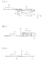
- the heat insulating plates (26, 26) are provided between the chip portion (20) and the printed circuit boards (25, 25), thereby further securing prevention of the printed circuit boards (25, 25) from being at high temperature by the heat radiation from the chip portion (20).
- Embodiment 2 Unlike internal heat insulation in Embodiment 1, heat conduction to an external substrate (43) is suppressed in a package (41) in which the chip (21) is sealed in Embodiment 2.
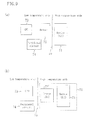
- Embodiment 4 refers to the case where a low temperature section (62) and a high temperature section (63) are formed according to operation temperatures of devices (66, 67) on a single printed circuit board (61), and are connected to each other by means of a pattern (64). In this case, heat generated at the high temperature section (63) is prevented from being transferred to the low temperature section (62) via the pattern (64) to prevent the low temperature section (62) from being at high temperature.
- Embodiment 4 in the case where a plurality of devices (66, 67) different in operable temperature from each other, for example, a device made of wide band gap semiconductor, such as SiC or the like and a device made of Si semiconductor are mounted on the same printed circuit board (61), and the high temperature section (63) of the device (67) operable at relatively high temperature and the low temperature section (62) of the device (66) operable at relatively low temperature are connected to each other by means of the pattern (64), the pattern (64) is elongated in length, or the resistor (65) is provided in the middle thereof.
- the heat resistance between the high temperature section (63) and the low temperature section (62) can be increased to enable suppression of temperature rise of the low temperature section (62) by the heat of the high temperature section (63).
- a driver section (72') for driving the device (71) is also made of wide band gap semiconductor, and the device (71) and the driver section (72) are accommodated in a single package (70). Because, it is preferable in view of loss and the like to arrange the driver section (72') for driving the device (71) near the device (71) as far as possible.
- the means for heat insulation is a heat insulating plate provided for suppressing heat radiation from the chip portion toward the peripheral component.
- the printed circuit board on which a component made of wide band gap semiconductor is mounted is divided into a high temperature section and a low temperature section according to operation temperatures of devices mounted thereon, and a pattern electrically connecting the high temperature section to the low temperature section on the printed circuit board is provided with heat transfer suppressing means.
- the wide band gap semiconductor is an SiC semiconductor.
Landscapes
- Engineering & Computer Science (AREA)
- Microelectronics & Electronic Packaging (AREA)
- Cooling Or The Like Of Semiconductors Or Solid State Devices (AREA)
- Inverter Devices (AREA)
- Cooling Or The Like Of Electrical Apparatus (AREA)
- Power Conversion In General (AREA)
Applications Claiming Priority (2)
| Application Number | Priority Date | Filing Date | Title |
|---|---|---|---|
| JP2006237050A JP2008060430A (ja) | 2006-08-31 | 2006-08-31 | 電力変換装置 |
| EP07805967A EP2058861A4 (de) | 2006-08-31 | 2007-08-22 | Elektrischer stromwandler |
Related Parent Applications (1)
| Application Number | Title | Priority Date | Filing Date |
|---|---|---|---|
| EP07805967.2 Division | 2007-08-22 |
Publications (2)
| Publication Number | Publication Date |
|---|---|
| EP2254151A2 true EP2254151A2 (de) | 2010-11-24 |
| EP2254151A3 EP2254151A3 (de) | 2011-10-12 |
Family
ID=39135768
Family Applications (3)
| Application Number | Title | Priority Date | Filing Date |
|---|---|---|---|
| EP10176557A Withdrawn EP2254151A3 (de) | 2006-08-31 | 2007-08-22 | Stromrichter |
| EP07805967A Ceased EP2058861A4 (de) | 2006-08-31 | 2007-08-22 | Elektrischer stromwandler |
| EP10176556A Withdrawn EP2348798A3 (de) | 2006-08-31 | 2007-08-22 | Stromrichter |
Family Applications After (2)
| Application Number | Title | Priority Date | Filing Date |
|---|---|---|---|
| EP07805967A Ceased EP2058861A4 (de) | 2006-08-31 | 2007-08-22 | Elektrischer stromwandler |
| EP10176556A Withdrawn EP2348798A3 (de) | 2006-08-31 | 2007-08-22 | Stromrichter |
Country Status (5)
| Country | Link |
|---|---|
| US (1) | US8030661B2 (de) |
| EP (3) | EP2254151A3 (de) |
| JP (1) | JP2008060430A (de) |
| CN (4) | CN102208400A (de) |
| WO (1) | WO2008026485A1 (de) |
Families Citing this family (27)
| Publication number | Priority date | Publication date | Assignee | Title |
|---|---|---|---|---|
| JP2009218416A (ja) * | 2008-03-11 | 2009-09-24 | Daikin Ind Ltd | 半導体回路 |
| JP5206102B2 (ja) * | 2008-05-08 | 2013-06-12 | トヨタ自動車株式会社 | 半導体装置 |
| JP4943373B2 (ja) * | 2008-05-09 | 2012-05-30 | 新日本製鐵株式会社 | デバイス実装方法 |
| WO2010073635A1 (ja) * | 2008-12-26 | 2010-07-01 | ダイキン工業株式会社 | 電力変換装置 |
| JP4687829B2 (ja) * | 2009-07-31 | 2011-05-25 | ダイキン工業株式会社 | 電力変換装置 |
| JP5472598B2 (ja) * | 2009-09-02 | 2014-04-16 | スタンレー電気株式会社 | 車両用灯具のled光源ユニット |
| JP5524234B2 (ja) * | 2009-11-06 | 2014-06-18 | 株式会社日立製作所 | ガスセンサ |
| JP5391162B2 (ja) * | 2010-08-17 | 2014-01-15 | 三菱電機株式会社 | 電力用半導体装置 |
| JP5484372B2 (ja) * | 2011-02-14 | 2014-05-07 | 三菱電機株式会社 | 半導体モジュール |
| JP5626087B2 (ja) * | 2011-04-13 | 2014-11-19 | 三菱電機株式会社 | 半導体装置 |
| DE102011107316A1 (de) * | 2011-07-06 | 2013-06-06 | Abb Ag | Anordnung zum Kühlen von Baugruppen eines Automatisierungs- oder Steuerungssystems |
| WO2013008424A1 (ja) | 2011-07-11 | 2013-01-17 | 三菱電機株式会社 | 電力用半導体モジュール |
| JP2013055198A (ja) * | 2011-09-02 | 2013-03-21 | Mitsubishi Electric Corp | 電力変換装置 |
| JP5858777B2 (ja) * | 2011-12-28 | 2016-02-10 | 三菱電機株式会社 | 空気調和装置 |
| JP6015405B2 (ja) * | 2012-12-12 | 2016-10-26 | 富士電機株式会社 | サーボアンプ |
| JP5482919B2 (ja) * | 2013-02-12 | 2014-05-07 | ダイキン工業株式会社 | 半導体回路 |
| JP6044703B2 (ja) * | 2013-03-18 | 2016-12-14 | 株式会社安川電機 | 電力変換装置 |
| US9433074B2 (en) * | 2013-04-29 | 2016-08-30 | Toyota Motor Engineering & Manufacturing North America, Inc. | Printed wiring boards having thermal management features and thermal management apparatuses comprising the same |
| WO2015025512A1 (ja) * | 2013-08-22 | 2015-02-26 | パナソニックIpマネジメント株式会社 | 駆動装置、電力変換装置、車両 |
| CN105376956B (zh) * | 2014-08-07 | 2017-12-15 | 艾默生网络能源有限公司 | 一种电路板的装配方法 |
| JP6424514B2 (ja) * | 2014-08-22 | 2018-11-21 | 富士電機株式会社 | 電力変換装置 |
| US10504813B2 (en) * | 2016-09-30 | 2019-12-10 | Astec International Limited | Heat sink assemblies for surface mounted devices |
| JP6544387B2 (ja) * | 2017-06-05 | 2019-07-17 | 株式会社デンソー | 電力変換装置 |
| JP6373468B1 (ja) * | 2017-10-19 | 2018-08-15 | 三菱電機株式会社 | パワーモジュール |
| CN108364940B (zh) * | 2018-02-24 | 2020-07-07 | 江西源能电气技术有限公司 | 一种电力用逆变电路装置 |
| JPWO2020174535A1 (ja) * | 2019-02-25 | 2021-09-13 | 三菱電機株式会社 | 回路基板、半導体装置、電力変換装置及び移動体 |
| JP7267412B2 (ja) * | 2019-05-27 | 2023-05-01 | 三菱電機株式会社 | 電力変換装置および電力変換装置の製造方法 |
Citations (2)
| Publication number | Priority date | Publication date | Assignee | Title |
|---|---|---|---|---|
| JP2004221381A (ja) * | 2003-01-16 | 2004-08-05 | Matsushita Electric Ind Co Ltd | 半導体装置 |
| JP2006042529A (ja) | 2004-07-28 | 2006-02-09 | Mitsubishi Electric Corp | 空気調和装置のインバータ制御装置 |
Family Cites Families (20)
| Publication number | Priority date | Publication date | Assignee | Title |
|---|---|---|---|---|
| FR2598252B1 (fr) * | 1986-05-05 | 1989-04-21 | Commissariat Energie Atomique | Connexions electriques a resistances thermique et electrique controlees. |
| JP2543452Y2 (ja) * | 1990-12-21 | 1997-08-06 | 富士通テン株式会社 | 半導体装置 |
| JP3157362B2 (ja) * | 1993-09-03 | 2001-04-16 | 株式会社東芝 | 半導体装置 |
| US5646444A (en) * | 1995-10-05 | 1997-07-08 | Motorola, Inc. | Apparatus and method for mounting a component to an electrical circuit |
| US5825625A (en) * | 1996-05-20 | 1998-10-20 | Hewlett-Packard Company | Heat conductive substrate mounted in PC board for transferring heat from IC to heat sink |
| US5739586A (en) * | 1996-08-30 | 1998-04-14 | Scientific-Atlanta, Inc. | Heat sink assembly including a printed wiring board and a metal case |
| SE508139C2 (sv) * | 1996-12-20 | 1998-08-31 | Ericsson Telefon Ab L M | Metod och anordning för anslutning av elektrisk komponent till kretskort |
| JPH1140901A (ja) * | 1997-07-23 | 1999-02-12 | Sharp Corp | 回路基板 |
| JP2001024294A (ja) * | 1999-07-09 | 2001-01-26 | Toyo Commun Equip Co Ltd | プリント配線基板 |
| US6549409B1 (en) * | 2000-08-21 | 2003-04-15 | Vlt Corporation | Power converter assembly |
| EP1239713B1 (de) * | 2001-03-07 | 2011-07-27 | Yazaki Corporation | Aus Substraten gestapelte Struktur |
| US20020154492A1 (en) * | 2001-04-24 | 2002-10-24 | Huang Kai Hung | Assembling structure of electronic device |
| JP4262453B2 (ja) * | 2002-07-15 | 2009-05-13 | 三菱電機株式会社 | 電力半導体装置 |
| US7786565B2 (en) * | 2003-09-04 | 2010-08-31 | Panasonic Corporation | Semiconductor apparatus including power semiconductor device constructed by using wide band gap semiconductor |
| JP2005174955A (ja) * | 2003-12-05 | 2005-06-30 | Toyota Industries Corp | 半導体モジュール |
| US8068346B2 (en) * | 2004-05-04 | 2011-11-29 | Hamilton Sundstrand Corporation | Circuit board with high density power semiconductors |
| FR2871022B1 (fr) * | 2004-05-25 | 2006-11-03 | Valeo Electronique Sys Liaison | Boitier pour circuits electriques ou electroniques |
| SE529673C2 (sv) * | 2004-09-20 | 2007-10-16 | Danaher Motion Stockholm Ab | Kretsarrangemang för kylning av ytmonterade halvledare |
| JP2006173243A (ja) * | 2004-12-14 | 2006-06-29 | Fujitsu Ten Ltd | プリント配線板、及びプリント回路板の放熱構造 |
| JP2006211805A (ja) * | 2005-01-27 | 2006-08-10 | Kansai Electric Power Co Inc:The | スイッチング装置 |
-
2006
- 2006-08-31 JP JP2006237050A patent/JP2008060430A/ja active Pending
-
2007
- 2007-08-22 CN CN2011101324466A patent/CN102208400A/zh active Pending
- 2007-08-22 EP EP10176557A patent/EP2254151A3/de not_active Withdrawn
- 2007-08-22 EP EP07805967A patent/EP2058861A4/de not_active Ceased
- 2007-08-22 CN CN2011101324451A patent/CN102208399A/zh active Pending
- 2007-08-22 WO PCT/JP2007/066265 patent/WO2008026485A1/ja not_active Ceased
- 2007-08-22 CN CN2011101322969A patent/CN102208398A/zh active Pending
- 2007-08-22 US US12/439,451 patent/US8030661B2/en not_active Expired - Fee Related
- 2007-08-22 CN CN2007800282222A patent/CN101496169B/zh not_active Expired - Fee Related
- 2007-08-22 EP EP10176556A patent/EP2348798A3/de not_active Withdrawn
Patent Citations (2)
| Publication number | Priority date | Publication date | Assignee | Title |
|---|---|---|---|---|
| JP2004221381A (ja) * | 2003-01-16 | 2004-08-05 | Matsushita Electric Ind Co Ltd | 半導体装置 |
| JP2006042529A (ja) | 2004-07-28 | 2006-02-09 | Mitsubishi Electric Corp | 空気調和装置のインバータ制御装置 |
Also Published As
| Publication number | Publication date |
|---|---|
| CN101496169B (zh) | 2011-10-05 |
| EP2254151A3 (de) | 2011-10-12 |
| CN102208400A (zh) | 2011-10-05 |
| CN102208398A (zh) | 2011-10-05 |
| EP2348798A3 (de) | 2011-10-12 |
| CN102208399A (zh) | 2011-10-05 |
| WO2008026485A1 (fr) | 2008-03-06 |
| US20090256161A1 (en) | 2009-10-15 |
| EP2058861A1 (de) | 2009-05-13 |
| EP2058861A4 (de) | 2011-10-12 |
| JP2008060430A (ja) | 2008-03-13 |
| CN101496169A (zh) | 2009-07-29 |
| EP2348798A2 (de) | 2011-07-27 |
| US8030661B2 (en) | 2011-10-04 |
Similar Documents
| Publication | Publication Date | Title |
|---|---|---|
| US8030661B2 (en) | Power conversion apparatus | |
| US10778113B2 (en) | Intelligent power module, electric vehicle, and hybrid car | |
| JP6513303B2 (ja) | 電力用半導体モジュールおよび電力変換装置 | |
| US7732917B2 (en) | Power module | |
| US8514579B2 (en) | Power semiconductor module including substrates spaced from each other | |
| KR101375502B1 (ko) | 전력용 반도체 모듈 | |
| CN106663677B (zh) | 电力变换装置 | |
| JP6033215B2 (ja) | パワーモジュール半導体装置 | |
| JP2012105419A (ja) | 電力変換装置 | |
| JP2009105389A (ja) | パワーモジュール | |
| JP2024014759A (ja) | 両面ヒートシンクを備える、表面実装ディスクリートデバイストップ面冷却ベースのパワーブロック | |
| US11545874B2 (en) | Thermal management assemblies for electronic assemblies circumferentially mounted around a motor using a flexible substrate | |
| JP6818873B2 (ja) | スイッチング素子駆動ユニット | |
| CN104518681A (zh) | 电力变换装置 | |
| JP3797040B2 (ja) | 半導体装置 | |
| JP2020141023A (ja) | 半導体装置 | |
| JP2012099855A (ja) | 電力変換装置 | |
| JP5851666B1 (ja) | 電力変換装置 | |
| JP2005073445A (ja) | スナバ回路部品及びこれを用いた電力変換装置 | |
| JP2012196140A (ja) | 電力変換装置 | |
| JP2017204910A (ja) | 圧縮機システム | |
| WO2025210370A1 (ja) | 電力変換装置 | |
| JP2009081976A (ja) | 電力変換装置 |
Legal Events
| Date | Code | Title | Description |
|---|---|---|---|
| PUAI | Public reference made under article 153(3) epc to a published international application that has entered the european phase |
Free format text: ORIGINAL CODE: 0009012 |
|
| 17P | Request for examination filed |
Effective date: 20100914 |
|
| AC | Divisional application: reference to earlier application |
Ref document number: 2058861 Country of ref document: EP Kind code of ref document: P |
|
| AK | Designated contracting states |
Kind code of ref document: A2 Designated state(s): AT BE BG CH CY CZ DE DK EE ES FI FR GB GR HU IE IS IT LI LT LU LV MC MT NL PL PT RO SE SI SK TR |
|
| AX | Request for extension of the european patent |
Extension state: AL BA HR MK RS |
|
| RAP1 | Party data changed (applicant data changed or rights of an application transferred) |
Owner name: DAIKIN INDUSTRIES, LIMITED |
|
| PUAL | Search report despatched |
Free format text: ORIGINAL CODE: 0009013 |
|
| AK | Designated contracting states |
Kind code of ref document: A3 Designated state(s): AT BE BG CH CY CZ DE DK EE ES FI FR GB GR HU IE IS IT LI LT LU LV MC MT NL PL PT RO SE SI SK TR |
|
| AX | Request for extension of the european patent |
Extension state: AL BA HR MK RS |
|
| RIC1 | Information provided on ipc code assigned before grant |
Ipc: H05K 1/02 20060101AFI20110902BHEP Ipc: H01L 25/07 20060101ALI20110902BHEP |
|
| STAA | Information on the status of an ep patent application or granted ep patent |
Free format text: STATUS: EXAMINATION IS IN PROGRESS |
|
| 17Q | First examination report despatched |
Effective date: 20170419 |
|
| STAA | Information on the status of an ep patent application or granted ep patent |
Free format text: STATUS: THE APPLICATION HAS BEEN WITHDRAWN |
|
| 18W | Application withdrawn |
Effective date: 20170719 |