EP2254152A2 - Festkörperschalteranordnung - Google Patents
Festkörperschalteranordnung Download PDFInfo
- Publication number
- EP2254152A2 EP2254152A2 EP10250948A EP10250948A EP2254152A2 EP 2254152 A2 EP2254152 A2 EP 2254152A2 EP 10250948 A EP10250948 A EP 10250948A EP 10250948 A EP10250948 A EP 10250948A EP 2254152 A2 EP2254152 A2 EP 2254152A2
- Authority
- EP
- European Patent Office
- Prior art keywords
- bus bar
- switch
- arrangement
- silicon carbide
- solid state
- Prior art date
- Legal status (The legal status is an assumption and is not a legal conclusion. Google has not performed a legal analysis and makes no representation as to the accuracy of the status listed.)
- Granted
Links
Images


Classifications
-
- H—ELECTRICITY
- H10—SEMICONDUCTOR DEVICES; ELECTRIC SOLID-STATE DEVICES NOT OTHERWISE PROVIDED FOR
- H10W—GENERIC PACKAGES, INTERCONNECTIONS, CONNECTORS OR OTHER CONSTRUCTIONAL DETAILS OF DEVICES COVERED BY CLASS H10
- H10W40/00—Arrangements for thermal protection or thermal control
- H10W40/20—Arrangements for cooling
- H10W40/22—Arrangements for cooling characterised by their shape, e.g. having conical or cylindrical projections
-
- H—ELECTRICITY
- H10—SEMICONDUCTOR DEVICES; ELECTRIC SOLID-STATE DEVICES NOT OTHERWISE PROVIDED FOR
- H10W—GENERIC PACKAGES, INTERCONNECTIONS, CONNECTORS OR OTHER CONSTRUCTIONAL DETAILS OF DEVICES COVERED BY CLASS H10
- H10W90/00—Package configurations
Definitions
- This application relates generally to switches, and more particularly, to a mounting arrangement of solid state switches.
- Switches perform switching functions within many types of units, such as power conversion units, motor control units, power switching units, and power distribution units, etc.
- the units often include solid state switches instead of mechanical based switches to avoid complications associated with moving components of the mechanical based switches. Switches, especially the solid state switches, generate thermal energy during operation.
- Interconnects are often incorporated into the unit to move thermal energy away from the switches. Undesirable results associated with incorporating the interconnects include added weight, increased packaging requirements, increased inductance, increased capacitance, increased assembly costs, and possible mechanical or electrical interconnect failures. The interconnects also resist movement of thermal energy. These results are especially undesirable in aerospace or space applications where the unit's excessive size and weight can impact performance of an airframe or spaceframe incorporating the unit.
- silicon solid state switches and germanium solid state switches are sometimes used instead of mechanical switches. These types of solid state switches are unable to operate at very high temperatures. Accordingly, units that include these solid state switches also include substantial cooling structures. These types of solid states switches are also bulky, which is especially disadvantageous in applications where excessive size and weight can impact performance, such as aerospace or space applications.
- An example solid state switching arrangement includes at least one bus bar configured to carry electrical current and at least one switch that is silicon carbide based.
- the switch is secured relative to the bus bar and the bus bar is configured to communicate thermal energy away from the switch.
- An example solid state switching arrangement includes at least one solid state switch, a first bus bar configured to carry electrical current, and a second bus bar configured to carry electrical current.
- the first bus bar is electrically isolated from the second bus bar.
- the at least one solid state switch includes a first switch portion directly mounted to the first bus bar and a second switch portion directly mounted to the second bus bar.
- An example method of arranging a switch includes mounting a silicon carbide based switch relative to a bus bar and communicating thermal energy away from the silicon carbide based switch using the bus bar.
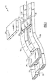
- Figure 1 shows an example mounting arrangement 10 including a multiple of switches 14 each having a portion mounted to a first bus bar 18a and a portion mounted to a second bus bar 18b.
- An insulating material 22 is positioned between the first bus bar 18a and the second bus bar 18b.
- the insulating material 22 electrically isolates the first bus bar 18a from the second bus bar 18b. Examples of the insulating material 22 include solids, liquids, gases, or a vacuum.
- control wires 26 facilitate electrical communication throughout the mounting arrangement 10.
- a plurality of bond wires 30 facilitate electrical and thermal communication between the switches 14, the first bus bar 18a, the second bus bar 18b, and the control wires 26.
- the example insulating material 22 is a solid material that holds control wires 26 away from the first bus bar 18a and the second bus bar 18b so that communications are routed through the bond wires 30.
- a cover 34 houses each of the switches 14.
- the cover 34 is a dam and fill type cover that encapsulates the switches 14, for example.
- the cover 34 is a dispensed liquid cover, or vapor deposition cover. These types of the cover 34 encapsulate the switches 14 and are typically used when the switches 14 are bare die switches. In some examples, a single one of the cover 34 protects more than one of the switches 14. Other protective arrangements are also possible.
- the switches 14, in this example, have a portion mounted directly to the first bus bar 18a and another portion mounted directly to the second bus bar 18b.
- Example techniques for directly mounting the switches 14 include metallurgically bonding or soldering the switches 14 to the bus bars 18a and 18b.
- Other examples include using a resin, epoxy, or mechanical attachment feature, such as a screw, to secure the switches 14 to the bus bars 18a and 18b.
- Wire bonding, ribbon bonding, lead frame bonding, via-in-silicon, beam bonding, and other methods could also be used to secure the switches 14 to the bus bars 18a and 18b, for example.
- the bus bars 18a and 18b include an interposer layer 36.
- the switches 14 are mounted directly to at least a portion of the interposer layer 36 that is incorporated into the bus bars 18a and 18b.
- the interposer layer 36 is configured to communicate thermal energy between the switches 14 and the bus bars 18a and 18b.
- the switches 14 are mounted to a printed wiring board in another example.
- mounting arrangements 42a and 42b each include one or more switches 54.
- a power supply 46 supplies power to the mounting arrangements 42a and 42b, which form a portion of a motor control unit 50, for example.
- the solid state switches 54 are silicon carbide based.
- the switches 54 are each mounted directly to one of the bus bars 18c, 18d, or 18e, which are each configured to carry electrical current within the motor control unit 50 between a first powered device 58a or 58b to a corresponding second powered device 58a or 58b.
- Bond wires 30 electrically connect the switches 54 on the bus bar 18c to the switches 54 on the bus bar 18d.
- the mounting arrangement 42a includes the bus bar 18c and the bus bar 18d.
- the mounting arrangement 42b includes the bus bar 18e.
- the example motor control unit 50 is used within an aircraft 62 for various functions, such as monitoring temperatures and vibrations of an aircraft engine 66.
- FIG. 3 and 4 show one of the switches 54 and a prior art switch 70.
- the switches 54 are silicon carbide switches, whereas the prior art switch 70 is a silicon switch.
- the switches 54 are each about 10 mm2 and can operate at temperatures of up to 225°C and voltages of up to 900 V.
- the prior art switch 70 is about 70 mm2 and can operate at temperatures of up to 150° C and voltages of up to 600 V.
- the switches 54 are operable at much higher temperatures than the prior art switch 70.
- the switches 54 are mounted directly to a bus bar 74 having a plurality of fins 78.
- the switches 54 generate thermal energy during operation, which moves from the switches 54 to the bus bar 74.
- the fins 78 facilitate moving thermal energy away from the bus bar 74 by increasing the surface area of the bus bar 74.
- features of the disclosed embodiments include mounting a silicon carbide based switch directly to a bus bar and using a silicon carbide based switch to perform electrical power switching functions. Another feature includes directly mounting a single switch to more than one bus bar to facilitate removing thermal energy from the switch.
Landscapes
- Inverter Devices (AREA)
- Gas-Insulated Switchgears (AREA)
Applications Claiming Priority (1)
| Application Number | Priority Date | Filing Date | Title |
|---|---|---|---|
| US12/468,110 US8724325B2 (en) | 2009-05-19 | 2009-05-19 | Solid state switch arrangement |
Publications (3)
| Publication Number | Publication Date |
|---|---|
| EP2254152A2 true EP2254152A2 (de) | 2010-11-24 |
| EP2254152A3 EP2254152A3 (de) | 2011-04-06 |
| EP2254152B1 EP2254152B1 (de) | 2020-02-26 |
Family
ID=42358058
Family Applications (1)
| Application Number | Title | Priority Date | Filing Date |
|---|---|---|---|
| EP10250948.6A Active EP2254152B1 (de) | 2009-05-19 | 2010-05-18 | Festkörperschalteranordnung und verfahren zum Anordnen eines Festkörperschalters |
Country Status (2)
| Country | Link |
|---|---|
| US (1) | US8724325B2 (de) |
| EP (1) | EP2254152B1 (de) |
Cited By (1)
| Publication number | Priority date | Publication date | Assignee | Title |
|---|---|---|---|---|
| WO2015165568A1 (de) * | 2014-04-30 | 2015-11-05 | Ellenberger & Poensgen Gmbh | Hochstromschalter |
Families Citing this family (2)
| Publication number | Priority date | Publication date | Assignee | Title |
|---|---|---|---|---|
| US9882357B2 (en) | 2015-06-26 | 2018-01-30 | Hamilton Sundstrand Corporation | Power distribution panel connector having thermal management feature |
| DE102016110847B4 (de) | 2016-06-14 | 2022-02-17 | Auto-Kabel Management Gmbh | Leitungsintegrierter Schalter und Verfahren zum Herstellen eines leitungsintegrierten Schalters |
Family Cites Families (35)
| Publication number | Priority date | Publication date | Assignee | Title |
|---|---|---|---|---|
| US3435891A (en) * | 1967-03-23 | 1969-04-01 | Int Rectifier Corp | Air flow baffle for rectifier heat exchanger |
| US3728585A (en) * | 1972-06-12 | 1973-04-17 | Gen Electric | Electric switchboard assembly with bus bar heat pipe means |
| EP0064856B1 (de) * | 1981-05-12 | 1986-12-30 | LUCAS INDUSTRIES public limited company | Multiphasen-Brückenanordnung |
| US4739448A (en) * | 1984-06-25 | 1988-04-19 | Magnavox Government And Industrial Electronics Company | Microwave multiport multilayered integrated circuit chip carrier |
| US4670817A (en) * | 1984-10-01 | 1987-06-02 | Venus Scientific Inc. | Heat sink and interconnection arrangement for series connected power diodes |
| US4748495A (en) | 1985-08-08 | 1988-05-31 | Dypax Systems Corporation | High density multi-chip interconnection and cooling package |
| US5275887A (en) * | 1986-04-22 | 1994-01-04 | Raychem Corporation | Fluoropolymer compositions |
| US5053920A (en) * | 1989-06-09 | 1991-10-01 | Digital Equipment Corporation | Integrated power conversion |
| FR2732156B1 (fr) * | 1995-03-23 | 1997-04-30 | Jakoubovitch A | Dispositif d'assemblage de condensateurs de puissance |
| FR2754669B1 (fr) | 1996-10-16 | 2002-04-12 | Alsthom Cge Alkatel | Module electronique de puissance, et systeme electronique de puissance comprenant une pluralite dudit module |
| US5930666A (en) | 1997-10-09 | 1999-07-27 | Astralux, Incorporated | Method and apparatus for packaging high temperature solid state electronic devices |
| US6319757B1 (en) | 1998-07-08 | 2001-11-20 | Caldus Semiconductor, Inc. | Adhesion and/or encapsulation of silicon carbide-based semiconductor devices on ceramic substrates |
| US6084764A (en) | 1998-12-21 | 2000-07-04 | Hamilton Sundstrand Corporation | Capacitor disconnecting assembly |
| US6036508A (en) | 1998-12-21 | 2000-03-14 | Hamilton Sundstrand Corporation | Connector for interconnecting a bus bar to a circuit board |
| US6278199B1 (en) * | 1999-02-25 | 2001-08-21 | International Rectifier Corp. | Electronic single switch module |
| US6470224B1 (en) | 1999-10-01 | 2002-10-22 | Hamilton Sundstrand Corporation | Configurable aircraft power system |
| US6215681B1 (en) * | 1999-11-09 | 2001-04-10 | Agile Systems Inc. | Bus bar heat sink |
| JP2001178146A (ja) | 1999-12-17 | 2001-06-29 | Keihin Corp | 携帯用発電機 |
| US6678182B2 (en) | 2000-11-07 | 2004-01-13 | United Defense Lp | Electrical bus with associated porous metal heat sink and method of manufacturing same |
| WO2002054449A2 (en) | 2001-01-03 | 2002-07-11 | Mississippi State University | Silicon carbide and related wide-bandgap transistors on semi-insulating epitaxy for high-speed, high-power applications |
| US6856045B1 (en) | 2002-01-29 | 2005-02-15 | Hamilton Sundstrand Corporation | Power distribution assembly with redundant architecture |
| JP3850739B2 (ja) | 2002-02-21 | 2006-11-29 | 三菱電機株式会社 | 半導体装置 |
| US6727436B2 (en) * | 2002-03-15 | 2004-04-27 | Memx, Inc. | Interconnect bus crossover for MEMS |
| JP4262453B2 (ja) | 2002-07-15 | 2009-05-13 | 三菱電機株式会社 | 電力半導体装置 |
| US6885553B2 (en) | 2002-09-27 | 2005-04-26 | Rockwell Automation Technologies, Inc. | Bus bar assembly for use with a compact power conversion assembly |
| US6822850B2 (en) | 2002-09-27 | 2004-11-23 | Rockwell Automation Technologies, Inc. | Laminated bus bar for use with a power conversion configuration |
| JP4039202B2 (ja) | 2002-10-16 | 2008-01-30 | 日産自動車株式会社 | 積層型半導体装置およびその組み立て方法 |
| JP4594237B2 (ja) | 2003-09-04 | 2010-12-08 | パナソニック株式会社 | 半導体装置 |
| US8068346B2 (en) | 2004-05-04 | 2011-11-29 | Hamilton Sundstrand Corporation | Circuit board with high density power semiconductors |
| US7281318B2 (en) | 2004-05-19 | 2007-10-16 | The Boeing Company | Method of manufacturing a composite structural member having an integrated electrical circuit |
| JP2006066582A (ja) | 2004-08-26 | 2006-03-09 | Sumitomo Electric Ind Ltd | 半導体装置、半導体モジュール及び半導体装置の製造方法 |
| US7330055B2 (en) * | 2004-10-26 | 2008-02-12 | Qortek, Inc. | Circuit with high power density applicability |
| JP4635564B2 (ja) | 2004-11-04 | 2011-02-23 | 富士電機システムズ株式会社 | 半導体装置 |
| JP2007305962A (ja) | 2006-05-12 | 2007-11-22 | Honda Motor Co Ltd | パワー半導体モジュール |
| US7916480B2 (en) | 2007-12-19 | 2011-03-29 | GM Global Technology Operations LLC | Busbar assembly with integrated cooling |
-
2009
- 2009-05-19 US US12/468,110 patent/US8724325B2/en active Active
-
2010
- 2010-05-18 EP EP10250948.6A patent/EP2254152B1/de active Active
Non-Patent Citations (1)
| Title |
|---|
| None |
Cited By (3)
| Publication number | Priority date | Publication date | Assignee | Title |
|---|---|---|---|---|
| WO2015165568A1 (de) * | 2014-04-30 | 2015-11-05 | Ellenberger & Poensgen Gmbh | Hochstromschalter |
| CN106465534A (zh) * | 2014-04-30 | 2017-02-22 | 埃伦贝格尔及珀恩斯根有限公司 | 大电流开关 |
| US10070514B2 (en) | 2014-04-30 | 2018-09-04 | Ellenberger & Poensgen Gmbh | High current switch |
Also Published As
| Publication number | Publication date |
|---|---|
| US20100296254A1 (en) | 2010-11-25 |
| EP2254152A3 (de) | 2011-04-06 |
| EP2254152B1 (de) | 2020-02-26 |
| US8724325B2 (en) | 2014-05-13 |
Similar Documents
| Publication | Publication Date | Title |
|---|---|---|
| KR101343140B1 (ko) | 3d 파워모듈 패키지 | |
| CN104425435B (zh) | 具有散热器的重叠模塑的基板‑芯片布置 | |
| EP2712040B1 (de) | Elektrische Schützanordnung mit Wärmeverwaltung | |
| EP2811642A1 (de) | Leistungswandler und verfahren zur herstellung eines leistungswandlers | |
| EP2854174B1 (de) | Halbleitervorrichtung und verfahren zur herstellung davon | |
| KR101669902B1 (ko) | 클립을 이용한 반도체 칩 패키지 및 그를 위한 제조방법 | |
| US9013065B2 (en) | Connecting mechanism arrangeable to a photovoltaic module | |
| JP2013514674A (ja) | 変速機制御装置として使用するため裸ダイ取付けにより重なり合って設けられる複数の印刷配線板層を持つ印刷配線板 | |
| EP2717285B1 (de) | Schutzschaltermodul | |
| EP3109957B1 (de) | Stromverteilungsanlage mit einem wärmevervaltungsmerkmal umfassenden schaltschutz | |
| EP2254152A2 (de) | Festkörperschalteranordnung | |
| US6912134B2 (en) | Fan control circuit and package | |
| EP1780791B1 (de) | Gehäuse für Leistungsschaltung und dessen Herstellungsverfahren | |
| KR20150031029A (ko) | 반도체 패키지 및 그 제조 방법 | |
| KR101713661B1 (ko) | 파워 모듈 패키지 | |
| EP2330622A1 (de) | Festkörperschalteranordnung | |
| WO2016156022A1 (en) | Apparatus comprising a power module attached through an isolation layer to an electric machine and corresponding manufacturing method | |
| KR20170068037A (ko) | 리드 프레임 일체형 파워 모듈 패키지 | |
| JP4961314B2 (ja) | パワー半導体装置 | |
| US10499514B2 (en) | Vehicular control device | |
| CN209562395U (zh) | 智能功率模块、空调器 | |
| Knörzer et al. | LTCC: A packaging technology suitable for high density integration and high temperature applications | |
| KR20160069902A (ko) | 전력 모듈 패키지 및 그 제조 방법 | |
| Neidig | Modules with Solder Contacts for High Power Applications |
Legal Events
| Date | Code | Title | Description |
|---|---|---|---|
| PUAI | Public reference made under article 153(3) epc to a published international application that has entered the european phase |
Free format text: ORIGINAL CODE: 0009012 |
|
| AK | Designated contracting states |
Kind code of ref document: A2 Designated state(s): AL AT BE BG CH CY CZ DE DK EE ES FI FR GB GR HR HU IE IS IT LI LT LU LV MC MK MT NL NO PL PT RO SE SI SK SM TR |
|
| AX | Request for extension of the european patent |
Extension state: BA ME RS |
|
| PUAL | Search report despatched |
Free format text: ORIGINAL CODE: 0009013 |
|
| AK | Designated contracting states |
Kind code of ref document: A3 Designated state(s): AL AT BE BG CH CY CZ DE DK EE ES FI FR GB GR HR HU IE IS IT LI LT LU LV MC MK MT NL NO PL PT RO SE SI SK SM TR |
|
| AX | Request for extension of the european patent |
Extension state: BA ME RS |
|
| RIC1 | Information provided on ipc code assigned before grant |
Ipc: H01L 23/36 20060101ALI20110225BHEP Ipc: H01L 25/07 20060101AFI20100803BHEP |
|
| 17P | Request for examination filed |
Effective date: 20111004 |
|
| 17Q | First examination report despatched |
Effective date: 20150302 |
|
| STAA | Information on the status of an ep patent application or granted ep patent |
Free format text: STATUS: EXAMINATION IS IN PROGRESS |
|
| RIC1 | Information provided on ipc code assigned before grant |
Ipc: H01L 25/07 20060101ALI20190617BHEP Ipc: H01L 23/00 20060101ALN20190617BHEP Ipc: H01L 23/367 20060101AFI20190617BHEP |
|
| REG | Reference to a national code |
Ref country code: DE Ref legal event code: R079 Ref document number: 602010063222 Country of ref document: DE Free format text: PREVIOUS MAIN CLASS: H01L0025070000 Ipc: H01L0023367000 |
|
| GRAP | Despatch of communication of intention to grant a patent |
Free format text: ORIGINAL CODE: EPIDOSNIGR1 |
|
| STAA | Information on the status of an ep patent application or granted ep patent |
Free format text: STATUS: GRANT OF PATENT IS INTENDED |
|
| RIC1 | Information provided on ipc code assigned before grant |
Ipc: H01L 23/00 20060101ALN20190806BHEP Ipc: H01L 23/367 20060101AFI20190806BHEP Ipc: H01L 25/07 20060101ALI20190806BHEP |
|
| RIC1 | Information provided on ipc code assigned before grant |
Ipc: H01L 23/00 20060101ALN20190829BHEP Ipc: H01L 23/367 20060101AFI20190829BHEP Ipc: H01L 25/07 20060101ALI20190829BHEP |
|
| INTG | Intention to grant announced |
Effective date: 20190911 |
|
| GRAS | Grant fee paid |
Free format text: ORIGINAL CODE: EPIDOSNIGR3 |
|
| GRAA | (expected) grant |
Free format text: ORIGINAL CODE: 0009210 |
|
| STAA | Information on the status of an ep patent application or granted ep patent |
Free format text: STATUS: THE PATENT HAS BEEN GRANTED |
|
| AK | Designated contracting states |
Kind code of ref document: B1 Designated state(s): AL AT BE BG CH CY CZ DE DK EE ES FI FR GB GR HR HU IE IS IT LI LT LU LV MC MK MT NL NO PL PT RO SE SI SK SM TR |
|
| REG | Reference to a national code |
Ref country code: GB Ref legal event code: FG4D |
|
| REG | Reference to a national code |
Ref country code: CH Ref legal event code: EP |
|
| REG | Reference to a national code |
Ref country code: AT Ref legal event code: REF Ref document number: 1238672 Country of ref document: AT Kind code of ref document: T Effective date: 20200315 |
|
| REG | Reference to a national code |
Ref country code: IE Ref legal event code: FG4D |
|
| REG | Reference to a national code |
Ref country code: DE Ref legal event code: R096 Ref document number: 602010063222 Country of ref document: DE |
|
| PG25 | Lapsed in a contracting state [announced via postgrant information from national office to epo] |
Ref country code: FI Free format text: LAPSE BECAUSE OF FAILURE TO SUBMIT A TRANSLATION OF THE DESCRIPTION OR TO PAY THE FEE WITHIN THE PRESCRIBED TIME-LIMIT Effective date: 20200226 Ref country code: NO Free format text: LAPSE BECAUSE OF FAILURE TO SUBMIT A TRANSLATION OF THE DESCRIPTION OR TO PAY THE FEE WITHIN THE PRESCRIBED TIME-LIMIT Effective date: 20200526 |
|
| REG | Reference to a national code |
Ref country code: NL Ref legal event code: MP Effective date: 20200226 |
|
| REG | Reference to a national code |
Ref country code: LT Ref legal event code: MG4D |
|
| PG25 | Lapsed in a contracting state [announced via postgrant information from national office to epo] |
Ref country code: LV Free format text: LAPSE BECAUSE OF FAILURE TO SUBMIT A TRANSLATION OF THE DESCRIPTION OR TO PAY THE FEE WITHIN THE PRESCRIBED TIME-LIMIT Effective date: 20200226 Ref country code: GR Free format text: LAPSE BECAUSE OF FAILURE TO SUBMIT A TRANSLATION OF THE DESCRIPTION OR TO PAY THE FEE WITHIN THE PRESCRIBED TIME-LIMIT Effective date: 20200527 Ref country code: HR Free format text: LAPSE BECAUSE OF FAILURE TO SUBMIT A TRANSLATION OF THE DESCRIPTION OR TO PAY THE FEE WITHIN THE PRESCRIBED TIME-LIMIT Effective date: 20200226 Ref country code: BG Free format text: LAPSE BECAUSE OF FAILURE TO SUBMIT A TRANSLATION OF THE DESCRIPTION OR TO PAY THE FEE WITHIN THE PRESCRIBED TIME-LIMIT Effective date: 20200526 Ref country code: IS Free format text: LAPSE BECAUSE OF FAILURE TO SUBMIT A TRANSLATION OF THE DESCRIPTION OR TO PAY THE FEE WITHIN THE PRESCRIBED TIME-LIMIT Effective date: 20200626 Ref country code: SE Free format text: LAPSE BECAUSE OF FAILURE TO SUBMIT A TRANSLATION OF THE DESCRIPTION OR TO PAY THE FEE WITHIN THE PRESCRIBED TIME-LIMIT Effective date: 20200226 |
|
| PG25 | Lapsed in a contracting state [announced via postgrant information from national office to epo] |
Ref country code: NL Free format text: LAPSE BECAUSE OF FAILURE TO SUBMIT A TRANSLATION OF THE DESCRIPTION OR TO PAY THE FEE WITHIN THE PRESCRIBED TIME-LIMIT Effective date: 20200226 |
|
| PG25 | Lapsed in a contracting state [announced via postgrant information from national office to epo] |
Ref country code: PT Free format text: LAPSE BECAUSE OF FAILURE TO SUBMIT A TRANSLATION OF THE DESCRIPTION OR TO PAY THE FEE WITHIN THE PRESCRIBED TIME-LIMIT Effective date: 20200719 Ref country code: LT Free format text: LAPSE BECAUSE OF FAILURE TO SUBMIT A TRANSLATION OF THE DESCRIPTION OR TO PAY THE FEE WITHIN THE PRESCRIBED TIME-LIMIT Effective date: 20200226 Ref country code: ES Free format text: LAPSE BECAUSE OF FAILURE TO SUBMIT A TRANSLATION OF THE DESCRIPTION OR TO PAY THE FEE WITHIN THE PRESCRIBED TIME-LIMIT Effective date: 20200226 Ref country code: DK Free format text: LAPSE BECAUSE OF FAILURE TO SUBMIT A TRANSLATION OF THE DESCRIPTION OR TO PAY THE FEE WITHIN THE PRESCRIBED TIME-LIMIT Effective date: 20200226 Ref country code: SM Free format text: LAPSE BECAUSE OF FAILURE TO SUBMIT A TRANSLATION OF THE DESCRIPTION OR TO PAY THE FEE WITHIN THE PRESCRIBED TIME-LIMIT Effective date: 20200226 Ref country code: EE Free format text: LAPSE BECAUSE OF FAILURE TO SUBMIT A TRANSLATION OF THE DESCRIPTION OR TO PAY THE FEE WITHIN THE PRESCRIBED TIME-LIMIT Effective date: 20200226 Ref country code: SK Free format text: LAPSE BECAUSE OF FAILURE TO SUBMIT A TRANSLATION OF THE DESCRIPTION OR TO PAY THE FEE WITHIN THE PRESCRIBED TIME-LIMIT Effective date: 20200226 Ref country code: RO Free format text: LAPSE BECAUSE OF FAILURE TO SUBMIT A TRANSLATION OF THE DESCRIPTION OR TO PAY THE FEE WITHIN THE PRESCRIBED TIME-LIMIT Effective date: 20200226 Ref country code: CZ Free format text: LAPSE BECAUSE OF FAILURE TO SUBMIT A TRANSLATION OF THE DESCRIPTION OR TO PAY THE FEE WITHIN THE PRESCRIBED TIME-LIMIT Effective date: 20200226 |
|
| REG | Reference to a national code |
Ref country code: AT Ref legal event code: MK05 Ref document number: 1238672 Country of ref document: AT Kind code of ref document: T Effective date: 20200226 |
|
| REG | Reference to a national code |
Ref country code: DE Ref legal event code: R097 Ref document number: 602010063222 Country of ref document: DE |
|
| REG | Reference to a national code |
Ref country code: DE Ref legal event code: R119 Ref document number: 602010063222 Country of ref document: DE |
|
| PLBE | No opposition filed within time limit |
Free format text: ORIGINAL CODE: 0009261 |
|
| STAA | Information on the status of an ep patent application or granted ep patent |
Free format text: STATUS: NO OPPOSITION FILED WITHIN TIME LIMIT |
|
| PG25 | Lapsed in a contracting state [announced via postgrant information from national office to epo] |
Ref country code: LI Free format text: LAPSE BECAUSE OF NON-PAYMENT OF DUE FEES Effective date: 20200531 Ref country code: AT Free format text: LAPSE BECAUSE OF FAILURE TO SUBMIT A TRANSLATION OF THE DESCRIPTION OR TO PAY THE FEE WITHIN THE PRESCRIBED TIME-LIMIT Effective date: 20200226 Ref country code: IT Free format text: LAPSE BECAUSE OF FAILURE TO SUBMIT A TRANSLATION OF THE DESCRIPTION OR TO PAY THE FEE WITHIN THE PRESCRIBED TIME-LIMIT Effective date: 20200226 Ref country code: CH Free format text: LAPSE BECAUSE OF NON-PAYMENT OF DUE FEES Effective date: 20200531 Ref country code: MC Free format text: LAPSE BECAUSE OF FAILURE TO SUBMIT A TRANSLATION OF THE DESCRIPTION OR TO PAY THE FEE WITHIN THE PRESCRIBED TIME-LIMIT Effective date: 20200226 |
|
| 26N | No opposition filed |
Effective date: 20201127 |
|
| PG25 | Lapsed in a contracting state [announced via postgrant information from national office to epo] |
Ref country code: SI Free format text: LAPSE BECAUSE OF FAILURE TO SUBMIT A TRANSLATION OF THE DESCRIPTION OR TO PAY THE FEE WITHIN THE PRESCRIBED TIME-LIMIT Effective date: 20200226 Ref country code: PL Free format text: LAPSE BECAUSE OF FAILURE TO SUBMIT A TRANSLATION OF THE DESCRIPTION OR TO PAY THE FEE WITHIN THE PRESCRIBED TIME-LIMIT Effective date: 20200226 |
|
| REG | Reference to a national code |
Ref country code: BE Ref legal event code: MM Effective date: 20200531 |
|
| PG25 | Lapsed in a contracting state [announced via postgrant information from national office to epo] |
Ref country code: LU Free format text: LAPSE BECAUSE OF NON-PAYMENT OF DUE FEES Effective date: 20200518 |
|
| PG25 | Lapsed in a contracting state [announced via postgrant information from national office to epo] |
Ref country code: IE Free format text: LAPSE BECAUSE OF NON-PAYMENT OF DUE FEES Effective date: 20200518 |
|
| PG25 | Lapsed in a contracting state [announced via postgrant information from national office to epo] |
Ref country code: DE Free format text: LAPSE BECAUSE OF NON-PAYMENT OF DUE FEES Effective date: 20201201 Ref country code: BE Free format text: LAPSE BECAUSE OF NON-PAYMENT OF DUE FEES Effective date: 20200531 |
|
| PG25 | Lapsed in a contracting state [announced via postgrant information from national office to epo] |
Ref country code: TR Free format text: LAPSE BECAUSE OF FAILURE TO SUBMIT A TRANSLATION OF THE DESCRIPTION OR TO PAY THE FEE WITHIN THE PRESCRIBED TIME-LIMIT Effective date: 20200226 Ref country code: MT Free format text: LAPSE BECAUSE OF FAILURE TO SUBMIT A TRANSLATION OF THE DESCRIPTION OR TO PAY THE FEE WITHIN THE PRESCRIBED TIME-LIMIT Effective date: 20200226 Ref country code: CY Free format text: LAPSE BECAUSE OF FAILURE TO SUBMIT A TRANSLATION OF THE DESCRIPTION OR TO PAY THE FEE WITHIN THE PRESCRIBED TIME-LIMIT Effective date: 20200226 |
|
| PG25 | Lapsed in a contracting state [announced via postgrant information from national office to epo] |
Ref country code: MK Free format text: LAPSE BECAUSE OF FAILURE TO SUBMIT A TRANSLATION OF THE DESCRIPTION OR TO PAY THE FEE WITHIN THE PRESCRIBED TIME-LIMIT Effective date: 20200226 Ref country code: AL Free format text: LAPSE BECAUSE OF FAILURE TO SUBMIT A TRANSLATION OF THE DESCRIPTION OR TO PAY THE FEE WITHIN THE PRESCRIBED TIME-LIMIT Effective date: 20200226 |
|
| P01 | Opt-out of the competence of the unified patent court (upc) registered |
Effective date: 20230522 |
|
| PGFP | Annual fee paid to national office [announced via postgrant information from national office to epo] |
Ref country code: GB Payment date: 20240419 Year of fee payment: 15 |
|
| PGFP | Annual fee paid to national office [announced via postgrant information from national office to epo] |
Ref country code: FR Payment date: 20240418 Year of fee payment: 15 |
|
| GBPC | Gb: european patent ceased through non-payment of renewal fee |
Effective date: 20250518 |
|
| PG25 | Lapsed in a contracting state [announced via postgrant information from national office to epo] |
Ref country code: GB Free format text: LAPSE BECAUSE OF NON-PAYMENT OF DUE FEES Effective date: 20250518 |
|
| PG25 | Lapsed in a contracting state [announced via postgrant information from national office to epo] |
Ref country code: FR Free format text: LAPSE BECAUSE OF NON-PAYMENT OF DUE FEES Effective date: 20250531 |