EP2255129B1 - Beleuchtungssystem, lichtquelle und elektrodenvorrichtung - Google Patents
Beleuchtungssystem, lichtquelle und elektrodenvorrichtung Download PDFInfo
- Publication number
- EP2255129B1 EP2255129B1 EP09711366.6A EP09711366A EP2255129B1 EP 2255129 B1 EP2255129 B1 EP 2255129B1 EP 09711366 A EP09711366 A EP 09711366A EP 2255129 B1 EP2255129 B1 EP 2255129B1
- Authority
- EP
- European Patent Office
- Prior art keywords
- auto
- electrode
- light source
- electrodes
- closing material
- Prior art date
- Legal status (The legal status is an assumption and is not a legal conclusion. Google has not performed a legal analysis and makes no representation as to the accuracy of the status listed.)
- Not-in-force
Links
- 239000000463 material Substances 0.000 claims description 39
- 229910052751 metal Inorganic materials 0.000 claims description 18
- 239000002184 metal Substances 0.000 claims description 18
- 229910045601 alloy Inorganic materials 0.000 claims description 14
- 239000000956 alloy Substances 0.000 claims description 14
- 229920001971 elastomer Polymers 0.000 claims description 11
- 230000008018 melting Effects 0.000 claims description 11
- 238000002844 melting Methods 0.000 claims description 11
- 239000005060 rubber Substances 0.000 claims description 11
- 239000007788 liquid Substances 0.000 claims description 6
- 239000007787 solid Substances 0.000 claims description 4
- GYHNNYVSQQEPJS-UHFFFAOYSA-N Gallium Chemical compound [Ga] GYHNNYVSQQEPJS-UHFFFAOYSA-N 0.000 claims description 3
- 239000011248 coating agent Substances 0.000 claims description 3
- 238000000576 coating method Methods 0.000 claims description 3
- 230000005294 ferromagnetic effect Effects 0.000 claims description 3
- 229910052733 gallium Inorganic materials 0.000 claims description 3
- 150000002739 metals Chemical class 0.000 claims description 3
- 229920002379 silicone rubber Polymers 0.000 claims description 3
- 229910000634 wood's metal Inorganic materials 0.000 claims description 3
- 230000005293 ferrimagnetic effect Effects 0.000 claims description 2
- 229910001084 galinstan Inorganic materials 0.000 claims description 2
- 229910052738 indium Inorganic materials 0.000 claims description 2
- APFVFJFRJDLVQX-UHFFFAOYSA-N indium atom Chemical compound [In] APFVFJFRJDLVQX-UHFFFAOYSA-N 0.000 claims description 2
- 229910001338 liquidmetal Inorganic materials 0.000 claims description 2
- 230000001681 protective effect Effects 0.000 claims description 2
- 230000005291 magnetic effect Effects 0.000 description 6
- 229910052736 halogen Inorganic materials 0.000 description 3
- 150000002367 halogens Chemical class 0.000 description 3
- 230000000149 penetrating effect Effects 0.000 description 3
- 239000003814 drug Substances 0.000 description 2
- 230000010354 integration Effects 0.000 description 2
- 239000011347 resin Substances 0.000 description 2
- 229920005989 resin Polymers 0.000 description 2
- PNEYBMLMFCGWSK-UHFFFAOYSA-N aluminium oxide Inorganic materials [O-2].[O-2].[O-2].[Al+3].[Al+3] PNEYBMLMFCGWSK-UHFFFAOYSA-N 0.000 description 1
- 239000012876 carrier material Substances 0.000 description 1
- 238000005266 casting Methods 0.000 description 1
- 238000005253 cladding Methods 0.000 description 1
- 239000012777 electrically insulating material Substances 0.000 description 1
- 239000007772 electrode material Substances 0.000 description 1
- 239000004744 fabric Substances 0.000 description 1
- 230000005307 ferromagnetism Effects 0.000 description 1
- 239000006261 foam material Substances 0.000 description 1
- 239000011888 foil Substances 0.000 description 1
- 238000005286 illumination Methods 0.000 description 1
- 238000002347 injection Methods 0.000 description 1
- 239000007924 injection Substances 0.000 description 1
- 239000012212 insulator Substances 0.000 description 1
- 238000012423 maintenance Methods 0.000 description 1
- 239000000203 mixture Substances 0.000 description 1
- 238000004382 potting Methods 0.000 description 1
- 229920002631 room-temperature vulcanizate silicone Polymers 0.000 description 1
- 238000000926 separation method Methods 0.000 description 1
- 239000000243 solution Substances 0.000 description 1
- 239000010935 stainless steel Substances 0.000 description 1
- 229910001220 stainless steel Inorganic materials 0.000 description 1
- 239000000126 substance Substances 0.000 description 1
- 230000000007 visual effect Effects 0.000 description 1
Images
Classifications
-
- F—MECHANICAL ENGINEERING; LIGHTING; HEATING; WEAPONS; BLASTING
- F21—LIGHTING
- F21V—FUNCTIONAL FEATURES OR DETAILS OF LIGHTING DEVICES OR SYSTEMS THEREOF; STRUCTURAL COMBINATIONS OF LIGHTING DEVICES WITH OTHER ARTICLES, NOT OTHERWISE PROVIDED FOR
- F21V21/00—Supporting, suspending, or attaching arrangements for lighting devices; Hand grips
- F21V21/002—Supporting, suspending, or attaching arrangements for lighting devices; Hand grips making direct electrical contact, e.g. by piercing
-
- F—MECHANICAL ENGINEERING; LIGHTING; HEATING; WEAPONS; BLASTING
- F21—LIGHTING
- F21S—NON-PORTABLE LIGHTING DEVICES; SYSTEMS THEREOF; VEHICLE LIGHTING DEVICES SPECIALLY ADAPTED FOR VEHICLE EXTERIORS
- F21S2/00—Systems of lighting devices, not provided for in main groups F21S4/00 - F21S10/00 or F21S19/00, e.g. of modular construction
-
- F—MECHANICAL ENGINEERING; LIGHTING; HEATING; WEAPONS; BLASTING
- F21—LIGHTING
- F21V—FUNCTIONAL FEATURES OR DETAILS OF LIGHTING DEVICES OR SYSTEMS THEREOF; STRUCTURAL COMBINATIONS OF LIGHTING DEVICES WITH OTHER ARTICLES, NOT OTHERWISE PROVIDED FOR
- F21V21/00—Supporting, suspending, or attaching arrangements for lighting devices; Hand grips
- F21V21/34—Supporting elements displaceable along a guiding element
- F21V21/35—Supporting elements displaceable along a guiding element with direct electrical contact between the supporting element and electric conductors running along the guiding element
-
- H—ELECTRICITY
- H01—ELECTRIC ELEMENTS
- H01R—ELECTRICALLY-CONDUCTIVE CONNECTIONS; STRUCTURAL ASSOCIATIONS OF A PLURALITY OF MUTUALLY-INSULATED ELECTRICAL CONNECTING ELEMENTS; COUPLING DEVICES; CURRENT COLLECTORS
- H01R13/00—Details of coupling devices of the kinds covered by groups H01R12/70 or H01R24/00 - H01R33/00
- H01R13/62—Means for facilitating engagement or disengagement of coupling parts or for holding them in engagement
- H01R13/6205—Two-part coupling devices held in engagement by a magnet
-
- F—MECHANICAL ENGINEERING; LIGHTING; HEATING; WEAPONS; BLASTING
- F21—LIGHTING
- F21V—FUNCTIONAL FEATURES OR DETAILS OF LIGHTING DEVICES OR SYSTEMS THEREOF; STRUCTURAL COMBINATIONS OF LIGHTING DEVICES WITH OTHER ARTICLES, NOT OTHERWISE PROVIDED FOR
- F21V23/00—Arrangement of electric circuit elements in or on lighting devices
- F21V23/06—Arrangement of electric circuit elements in or on lighting devices the elements being coupling devices, e.g. connectors
-
- H—ELECTRICITY
- H01—ELECTRIC ELEMENTS
- H01R—ELECTRICALLY-CONDUCTIVE CONNECTIONS; STRUCTURAL ASSOCIATIONS OF A PLURALITY OF MUTUALLY-INSULATED ELECTRICAL CONNECTING ELEMENTS; COUPLING DEVICES; CURRENT COLLECTORS
- H01R4/00—Electrically-conductive connections between two or more conductive members in direct contact, i.e. touching one another; Means for effecting or maintaining such contact; Electrically-conductive connections having two or more spaced connecting locations for conductors and using contact members penetrating insulation
- H01R4/24—Connections using contact members penetrating or cutting insulation or cable strands
- H01R4/2404—Connections using contact members penetrating or cutting insulation or cable strands the contact members having teeth, prongs, pins or needles penetrating the insulation
- H01R4/2406—Connections using contact members penetrating or cutting insulation or cable strands the contact members having teeth, prongs, pins or needles penetrating the insulation having needles or pins
Definitions
- the invention relates to a system as defined in the pre-characterizing part of claim 1.
- the invention further relates to an electrode device, as defined in claim 12, adapted for use in the system according to the invention.
- Dipline lit panel systems operate at low voltages, for example, 12 V or 24V. These known systems are promoted as self-powered, flat, flexible panels which serve as electrified walls or ceiling surfaces. It allows simple placement of light sources anywhere on a flat surface and has them light up instantly.
- SLS relatively small light sources
- LED products or miniature halogen lamps have entered the market.
- SLS light sources
- Most of these products are retrofit so that they can be integrated in a current infrastructure with minimal investment.
- This poses limitations on exploiting the full potential of SLS.
- Especially new buildings or homes provide the possibility of breaking away from the existing paradigms in lighting design.
- slim SLS lighting systems allow unobtrusive integration of lighting into a building.
- SLS-based systems also require new solutions for heat management, driver infrastructure, mechanical fixtures and user interfacing.
- One of the key value drivers of SLS integration in domestic environments is freedom of positioning.
- a consumer can create any desired lighting pattern by placing an SLS lighting system at any position on a wall or ceiling. Moreover, it is possible for a consumer to create his own atmosphere at home by combining several of these systems. In order that such a system works properly, it should allow easy positioning, fixation, and instant operation, and it should be robust.
- the known electrode device is a panel, and its electrodes are plate-shaped electrodes which are arranged in a stacked position.
- the plate electrodes are separated by a plate-shaped electrically insulating layer and each plate electrode is preferably covered by a decorative (and electrically insulating) layer.
- the panels have typical dimensions of 1 square meter and a thickness of about 3 cm.
- the electrode device can be used to form façade walls or ceilings, or it can be alternatively applied as a cladding on existing walls, ceilings, or floors.
- the electrode device is connected to an electric energy supply system.
- the light sources which are suitable for use in the known system, have pin-shaped electric contacts which are able to pierce the plate-shaped-electrodes and the intermediate electrically insulating layer.
- the pin-shaped electric contacts have different lengths so that, upon placing a light source on the electrode device, one electrode penetrates both plate electrodes and the other electrode penetrates only one plate electrode, thus realizing an appropriate electric contact with the electrode device.
- the pin-shaped electric contact penetrating both plate electrodes is partly coated with an electrically insulating layer so as to prevent short-circuiting of the two plate electrodes via this electric contact.
- Document EP 0 109 852 discloses a system according to the preamble of claim 1 and an electrode device according to the preamble of claim 12.
- the system as described in the opening paragraph is defined by the characterizing part of claim 1.
- the electrode material When the light source is mounted on the electrode device, the electrode material will get damaged because it is pierced by relatively small piercing objects, for example, pin-shaped contact elements of the light source.
- An auto-closing material is understood to be a material that restores itself in such a way that its surface can be considered to be effectively closed, i.e. after the auto-closing material has restored itself, liquid or paste material cannot flow freely through the damaged spots, or the damaged spots have even disappeared.
- the material may restore itself when the piercing object is still present and/or after it has been removed.
- Very suitable auto-closing materials are found among the group of materials consisting of rubber, low melting point metals/alloys, liquid metals/alloys, and metal/alloy pastes.
- the use of auto-closing rubber material as well as suitable rubber materials is known from medical applications, for example, a medicine bottle from which a small quantity of medicine is to be extracted via an injection needle piercing a rubber closure of such a bottle.
- Liquids and paste materials are capable of flowing freely and will thus auto-close, or in other words, fill up an open space which is left after a piercing element has been removed.
- a low melting point material is understood to be a material that is solid at room temperature, i.e. 20°C to 25°C, but will become liquid due to the heat generated by the light source during operation and will thus maintain a reliable electric contact during operation. This material is capable of restoring itself to its original state when it is heated by the light source.
- Said melting points are preferably in the range of 30°C to 200°C, or 30°C to 120°C, or 50°C to 80°C.
- Materials known to exhibit at least one of above-mentioned properties are Gallium, Indium, Ga68In20Sn12, Indalloy 117, SnPbInBi, Woods metal, Indalloy IE, and silicon rubbers.
- the chemical composition, melting points and thermal conductivity of these metals/alloys are well known in the art.
- the system according to the invention is characterized in that the auto-closing material is chosen from the group consisting of metal/alloy paste, metal/alloys that are liquid at room temperature such as Galinstan, and is contained in between two auto-closing, solid layers. It is thus counteracted that the free-flowing materials can flow out of the system to the exterior, which improves the maintenance of the system.
- the electrode is embodied, for example, as a metal plate electrode or as a metal mesh cloth. If the auto-closing rubber faces the light source in its mounted position, it automatically gives the system a more aesthetic appearance after removal of the light source than is the case for a system with bare metal plate electrodes.
- the system is characterized in that the electrodes comprise at least one ferrimagnetic, ferromagnetic or electromagnetic material. Easy mounting of the light source on the electrode device is attained when both electrodes are made of a magnetizable, permanent magnetic or electromagnetic material, and when the base of the light source is provided with a magnetizable, permanent magnetic or an electromagnetic adhesion device. The requirement imposed on the electric contacts of the lamp to be long and thick enough to mechanically fix the light source on the electrode device is thus no longer applicable; fixation of the light source on the electrode device is realized via magnetic adhesion instead.
- an embodiment of the system is characterized in that the electrically conducting, auto-closing material and/or the electrically insulating layer has a thermal conductivity of at least 1W/Mk which is suitable for layers having a thickness of 2.5 mm or less, but preferably more than 10 W/Mk which is suitable for layers having a thickness up to 20 mm.
- the electrically insulating layer preferably has only a limited thickness of, for example, 5 mm.
- the electrically insulating layer should have a thickness of at least 1 mm to counteract short-circuiting between the two electrodes of the electrode device, and thus to ensure a reliable separation between these electrodes.
- suitable materials are preferably chosen from the group consisting of thermally enhanced but electrically insulating materials such as are known in the field of thermal interface materials, for example, tabular alumina filled casting resin CC3-300 or thermally conductive, low-viscosity potting resin CC3-301AD-FR as available from Cast-Coat Inc.
- the system is characterized in that a protective and/or aesthetic screen is provided on the electrode closest to the light source in the mounted position and on a surface of said electrode facing the light source.
- a protective and/or aesthetic screen is provided on the electrode closest to the light source in the mounted position and on a surface of said electrode facing the light source.
- the invention further relates to an device, as defined in claim 12.
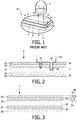
- the electrode device 1 is an electrically insulating plate 2 having both its main surfaces covered with thin metal foils which constitute a first electrode 3 and a second electrode 4. For mechanical and, optionally, aesthetic reasons, each electrode is covered with a respective screen 5, 6.
- the known electrode device typically has a thickness T of about 25 mm and the electrically insulating plate and screens are typically made of foam material.
- a light source 7 is mechanically mountable onto the electrode device 1 via a first electric contact 8 and a second electric contact 9.
- the first electric contact 8 is relatively short so that it cannot reach the second electrode 4 but can only pierce it and thus establish an electric connection with the first electrode 3.
- the second electric contact 9 is relatively long and can thus pierce both electrodes 3 and 4, thus establishing an electric connection with the second electrode.
- the second electric contact is partly provided with an electrically insulating layer 10.
- Fig. 2 is a cross-section of an electrode device 1 applicable in a system. Similarly as in the prior-art system, the light source is to be mounted on the electrode device.
- the first and the second electrode sheet are separated by an electrically insulating layer 25 made of a suitable thermal interface material, for example, thermally conductive RTV silicon rubber CC3-1200 as available from Cast-Coat inc.
- the electrode device thus has a total thickness T of less than 5 mm.
- the ferromagnetism of the electrode sheets allows the light source to be mounted onto the electrode device via magnetic adhesion, provided that the light source has a base with magnetizable elements (see Fig. 5 ).
- the light source 26 is roughly indicated in Fig. 2 with a first contact element 27 penetrating the first electrode sheet and a second contact element 28 penetrating both the first and the second electrode sheet, the second contact element being provided with an electrically insulating coating 29 so as to avoid short-circuiting of the two electrode sheets 23, 24.
- the light source may be a miniature halogen lamp, for example, one or more halogen lamps each having a nominal power of, for example, 20W during operation, or it may be a LED or a plurality of LEDs each having a nominal power of, for example, about 3W.
- the electrode device 1 is a seven-layer structure.
- Two electrode layers 31, 32 are embodied as metal paste, for example, metal-filled pastes which are used to connect heat sinks to microprocessors, each electrode layer being contained in between two respective auto-closing silicon rubber layers 33,34,35,36, for which purpose two respective auto-closing rubber layers at each end of each electrode layer are mutually connected via a closing element 38.
- a central layer 37 is provided as an insulator between the electrodes and gives the electrode device its form stability.
- the electrically insulating layer is relatively thick, for example, 1.5 cm, so as to allow mechanical fixation of the light source on the electrode device via pin-shaped contact elements of the light source.
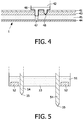
- the electrode device 1 shown in Fig.4 comprises four layers.
- An aesthetic screen top layer 41 faces the mounted light source 42.
- Two electrodes 43, 44 are made of a low melting point material, for example, Woods metal having a melting point of about 70°C, or InCuBi alloy having a melting point of 58°C, or Gallium metal having a melting point of 30°C.
- An electrically insulating but thermally conductive layer 45, made of a suitable thermal interface material is present between the two electrode layers 43,44. During operation, the mounted lamp generates heat which is transferred from the lamp base 46 to the electrode device.
- the low melting point material of the electrodes will melt locally adjacent the lamp base and/or contact elements and thus "wet" the pin-shaped electric contact elements 47, 48 of the light source. A satisfactory electric contact between the electrodes and the contact elements is thus ensured.
- the system cools down and the low melting point material solidifies again.
- Fig. 5 is a cross-sectional side view of the lamp base 51 of a light source.
- the base comprises at least two permanent magnetic or magnetizable elements, namely, two permanent magnets 52 in Fig.5 .
- the magnets are placed flush with the bottom 53 of the lamp base. Once mechanically connected, the lamp base will be stuck and held by magnetic force.
- Additional elements of the lamp base are at least two electric contacts 54 placed adjacent or at close distance to the magnets.
- Each electrode has a sharp, pin-shaped end 55 which extends from the bottom of the lamp base by a small distance and can pierce the various layers of the electrode device. The electric connection between the electrode device and the light source is established in this way.
Landscapes
- Engineering & Computer Science (AREA)
- General Engineering & Computer Science (AREA)
- Arrangement Of Elements, Cooling, Sealing, Or The Like Of Lighting Devices (AREA)
- Non-Portable Lighting Devices Or Systems Thereof (AREA)
- Illuminated Signs And Luminous Advertising (AREA)
- Electroluminescent Light Sources (AREA)
Claims (12)
- System, eine Elektrodenvorrichtung (1) und eine Lichtquelle zum Ausstrahlen von Licht umfassend,
wobei die Lichtquelle eine Basis (46, 51) mit einer Basisoberfläche umfasst, auf der zumindest zwei Kontaktelemente (47, 48, 54) bereitgestellt sind,
wobei die Elektrodenvorrichtung zumindest zwei Elektroden in einer gestapelten Position aufweist, und die durch eine elektrisch isolierende Schicht (37) getrennt sind, wobei die besagten beiden Elektroden während des Betriebs eine unterschiedliche Polarität aufweisen,
wobei zumindest eine Elektrode ein elektrisch leitendes, selbstschließendes Material (31, 32) umfasst,
dadurch gekennzeichnet, dass das selbstschließende Material (31, 32) für die zumindest eine Elektrode aus der Gruppe ausgewählt wird, die Metall-/ Legierungspaste, Metall-/ Legierungsflüssigkeit umfasst und zwischen zwei selbstschließenden festen Schichten (33, 34, 35, 36) enthalten ist. - System nach Anspruch 1, dadurch gekennzeichnet, dass das elektrisch leitende, selbstschließende Material aus der Gruppe ausgewählt wird, die Kautschuk, Metalle/ Legierungen mit einem niedrigen Schmelzpunkt, flüssige Metalle/ Legierungen und Metall-/ Legierungspasten umfasst.
- System nach Anspruch 1, dadurch gekennzeichnet, dass das elektrisch leitende, selbstschließende Material einen spezifischen Durchgangswiderstand von
<= 1 Ohm/ cm aufweist. - System nach Anspruch 1, dadurch gekennzeichnet, dass das leitende, selbstschließende Material Kautschuk ist und als Beschichtung auf zumindest einer Elektrode bereitgestellt wird.
- System nach Anspruch 1, dadurch gekennzeichnet, dass die Elektroden zumindest ein ferrimagnetisches, ferromagnetisches oder elektromagnetisches Material umfassen.
- System nach Anspruch 1, dadurch gekennzeichnet, dass das elektrisch leitende, selbstschließende Material eine thermische Leitfähigkeit von zumindest 1 W/mK, vorzugsweise von zumindest 10 W/mK aufweist.
- System nach Anspruch 1, dadurch gekennzeichnet, dass das elektrisch leitende, selbstschließende Material aus der Gruppe ausgewählt wird, die Gallium, Indium, Galinstan, Ga68In20Sn12, Indalloy 117, SnPbInBi, Woodmetall, Indalloy 1E und Silikonkautschuke umfasst.
- System nach Anspruch 1, dadurch gekennzeichnet, dass die elektrisch isolierende Schicht eine thermische Leitfähigkeit von zumindest 1 W/mK, vorzugsweise von zumindest 10 W/mK aufweist.
- System nach Anspruch 8, dadurch gekennzeichnet, dass die elektrisch isolierende Schicht aus der Gruppe ausgewählt wird, die aus Thermal-Interface-Materialien besteht, die als Lückenfüller bekannt sind.
- System nach Anspruch 8, dadurch gekennzeichnet, dass die elektrisch isolierende Schicht eine Dicke in der Größenordnung zwischen 1 und 5 mm aufweist.
- System nach Anspruch 1, dadurch gekennzeichnet, dass auf der Elektrode ein schützender / ästhetischer Schirm am nächsten zur Lichtquelle in einer montierten Position und auf einer Oberfläche der besagten Elektrode gegenüber der Lichtquelle bereitgestellt wird.
- Elektrodenvorrichtung, die zumindest zwei Elektroden in einer gestapelten Position aufweist, und die durch eine elektrisch isolierende Schicht (37) getrennt sind, wobei die besagten beiden Elektroden während des Betriebs eine unterschiedliche Polarität aufweisen, wobei zumindest eine Elektrode ein elektrisch leitendes, selbstschließendes Material (31, 32) umfasst, dadurch gekennzeichnet, dass das selbstschließende Material (31, 32) für die zumindest eine Elektrode aus der Gruppe ausgewählt wird, die Metall-/ Legierungspaste, Metall-/ Legierungsflüssigkeit umfasst und zwischen zwei selbstschließenden festen Schichten (33, 34, 35, 36) enthalten ist.
Priority Applications (1)
| Application Number | Priority Date | Filing Date | Title |
|---|---|---|---|
| EP09711366.6A EP2255129B8 (de) | 2008-02-14 | 2009-02-09 | Beleuchtungssystem, lichtquelle und elektrodenvorrichtung |
Applications Claiming Priority (3)
| Application Number | Priority Date | Filing Date | Title |
|---|---|---|---|
| EP08151421 | 2008-02-14 | ||
| EP09711366.6A EP2255129B8 (de) | 2008-02-14 | 2009-02-09 | Beleuchtungssystem, lichtquelle und elektrodenvorrichtung |
| PCT/IB2009/050503 WO2009101561A1 (en) | 2008-02-14 | 2009-02-09 | Lighting system, light source and electrode device |
Publications (3)
| Publication Number | Publication Date |
|---|---|
| EP2255129A1 EP2255129A1 (de) | 2010-12-01 |
| EP2255129B1 true EP2255129B1 (de) | 2016-07-20 |
| EP2255129B8 EP2255129B8 (de) | 2016-09-21 |
Family
ID=40719997
Family Applications (1)
| Application Number | Title | Priority Date | Filing Date |
|---|---|---|---|
| EP09711366.6A Not-in-force EP2255129B8 (de) | 2008-02-14 | 2009-02-09 | Beleuchtungssystem, lichtquelle und elektrodenvorrichtung |
Country Status (5)
| Country | Link |
|---|---|
| US (1) | US8390184B2 (de) |
| EP (1) | EP2255129B8 (de) |
| JP (1) | JP5575665B2 (de) |
| CN (1) | CN101946122B (de) |
| WO (1) | WO2009101561A1 (de) |
Families Citing this family (26)
| Publication number | Priority date | Publication date | Assignee | Title |
|---|---|---|---|---|
| EP2245361A1 (de) * | 2008-02-14 | 2010-11-03 | Koninklijke Philips Electronics N.V. | Beleuchtungssystem, elektrodenvorrichtung und lichtquelle |
| DE102010000346A1 (de) * | 2010-02-09 | 2011-08-11 | Hettich-Heinze GmbH & Co. KG, 32139 | Anordnung eines Beschlagelementes zur Montage eines Stromverbrauchers an einer Leichtbauplatte, Leichtbauplatte, Beschlagelement und Stromversorgungsbauteil |
| ITBO20100465A1 (it) * | 2010-07-22 | 2012-01-23 | Viabizzuno Srl | Apparato di illuminazione a configurazione variabile. |
| US8668361B2 (en) | 2010-09-22 | 2014-03-11 | Bridgelux, Inc. | LED-based replacement for fluorescent light source |
| US8227813B2 (en) | 2010-09-22 | 2012-07-24 | Bridgelux, Inc. | LED light source utilizing magnetic attachment |
| RU2614515C2 (ru) | 2011-12-05 | 2017-03-28 | Филипс Лайтинг Холдинг Б.В. | Осветительная система |
| DE102012211546B4 (de) * | 2012-07-03 | 2017-02-16 | Morpho Cards Gmbh | Chipkarte mit bei Raumtemperatur pastenförmiger oder flüssiger Kontaktierung |
| DE102012211757A1 (de) * | 2012-07-05 | 2014-01-23 | Kiekert Ag | Verfahren für ein Verbinden einer elektrischen Komponente mit einem Komponententräger nebst Vorrichtung |
| EP2690233A1 (de) * | 2012-07-24 | 2014-01-29 | Tarkett GDL S.A. | Mehrschichtige Oberflächenbeschichtung |
| US10132452B2 (en) | 2013-03-14 | 2018-11-20 | Apex Technologies, Inc. | Suspended track and planar electrode systems and methods |
| US10680383B2 (en) | 2013-03-14 | 2020-06-09 | Apex Technologies, Inc. | Linear electrode systems for module attachment with non-uniform axial spacing |
| US9754519B2 (en) | 2013-09-27 | 2017-09-05 | Alf Operating Partners, Ltd. | Composite street sign with integral electrical wiring and integrated power supply |
| US9286813B2 (en) * | 2013-09-27 | 2016-03-15 | Alf Operating Partners, Ltd. | Composite street sign with integral electrical wiring |
| JP6312862B2 (ja) * | 2014-05-20 | 2018-04-18 | フィリップス ライティング ホールディング ビー ヴィ | 共形コーティングされた照明又はイルミネーションシステム |
| WO2018182678A1 (en) * | 2017-03-31 | 2018-10-04 | Intel Corporation | Thermally resistive capping layers in a resistive switch device |
| US10897114B2 (en) * | 2018-02-22 | 2021-01-19 | Light Corp Inc. | Configurable low voltage power panel |
| FR3084442B1 (fr) | 2018-07-24 | 2021-01-15 | Kaiwen Consulting | Enseigne lumineuse presentant un cablage electrique a structure verticale |
| US11056822B2 (en) * | 2019-07-23 | 2021-07-06 | International Business Machines Corporation | Power socket module and plug |
| CN110707446A (zh) * | 2019-10-08 | 2020-01-17 | 赛尔富电子有限公司 | 一种防水轨道式取电系统和供电货架 |
| CH717125A1 (de) * | 2020-02-13 | 2021-08-16 | Visplay Int Ag | Warentragsystem mit flexiblem Stromabgriff. |
| US11240903B2 (en) | 2020-02-27 | 2022-02-01 | Light Corp Inc. | Ceiling panel system with wireless control of connected lighting modules |
| EP4139605A1 (de) * | 2020-04-22 | 2023-03-01 | Laser Design Srl | Verbesserung eines elektrischen stromversorgungssystems zur erzeugung von anzeigeeinheiten, leuchtzeichen und dergleichen |
| FI20206155A1 (fi) * | 2020-11-13 | 2022-05-14 | Absolute Module Oy | Rakennejärjestelmä |
| US12111050B2 (en) * | 2021-07-29 | 2024-10-08 | Signify Holding B.V. | Laser lighting device |
| EP4699416A2 (de) * | 2023-04-20 | 2026-02-25 | Bocci Design & Manufacturing, Inc. | Schichtverbundmaterial und system für geräteaufhängung und elektrische verbindung |
| EP4644765A1 (de) * | 2024-04-30 | 2025-11-05 | the best way GmbH | Elektrogerät mit einer metall-kunststoff-verbundplatte |
Family Cites Families (10)
| Publication number | Priority date | Publication date | Assignee | Title |
|---|---|---|---|---|
| BE571881A (de) * | ||||
| EP0109852A3 (de) * | 1982-11-23 | 1984-12-05 | University College Cardiff Consultants Ltd. | Anzeigevorrichtung |
| FR2540683B1 (fr) | 1983-02-04 | 1989-01-06 | Assistance Maintenance Const E | Dispositif d'alimentation d'un recepteur electrique a position variable sur une surface |
| US5010463A (en) * | 1990-04-30 | 1991-04-23 | Ross David L | Electrified bulletin board with illuminable push-pin |
| FR2752640B1 (fr) * | 1996-08-21 | 1998-11-06 | Jolly Andre Jean | Procede de fabrication d'un panneau sandwich a ames conductrices a haute resilience et panneau obtenu |
| IT249532Y1 (it) * | 2000-06-06 | 2003-05-19 | Pininfarina Extra Srl | Dispositivo luminoso. |
| JP2005191520A (ja) * | 2003-06-30 | 2005-07-14 | Fujisaki Denki Kk | 照明装置と発光ダイオード用の電源供給装置及びこの電源供給装置に使用する導電ボード |
| JP2005312444A (ja) * | 2004-03-31 | 2005-11-10 | Prestige:Kk | 植物育成装置と植物生育方法 |
| JP2006210336A (ja) * | 2004-12-28 | 2006-08-10 | Fujisaki Denki Kk | 発光ダイオードの照明装置 |
| CA2614982A1 (en) * | 2005-07-14 | 2007-01-18 | Tir Technology Lp | Power board and plug-in lighting module |
-
2009
- 2009-02-09 US US12/866,294 patent/US8390184B2/en not_active Expired - Fee Related
- 2009-02-09 WO PCT/IB2009/050503 patent/WO2009101561A1/en not_active Ceased
- 2009-02-09 EP EP09711366.6A patent/EP2255129B8/de not_active Not-in-force
- 2009-02-09 CN CN200980105121.XA patent/CN101946122B/zh not_active Expired - Fee Related
- 2009-02-09 JP JP2010546427A patent/JP5575665B2/ja not_active Expired - Fee Related
Also Published As
| Publication number | Publication date |
|---|---|
| WO2009101561A1 (en) | 2009-08-20 |
| CN101946122B (zh) | 2014-12-31 |
| JP5575665B2 (ja) | 2014-08-20 |
| EP2255129A1 (de) | 2010-12-01 |
| EP2255129B8 (de) | 2016-09-21 |
| JP2011517010A (ja) | 2011-05-26 |
| CN101946122A (zh) | 2011-01-12 |
| US20100320896A1 (en) | 2010-12-23 |
| US8390184B2 (en) | 2013-03-05 |
Similar Documents
| Publication | Publication Date | Title |
|---|---|---|
| EP2255129B1 (de) | Beleuchtungssystem, lichtquelle und elektrodenvorrichtung | |
| US8922121B2 (en) | Lighting system, electrode device and light source | |
| CN102037616B (zh) | 电导磁耦合系统 | |
| EP2577153B1 (de) | Beleuchtungskörper für led-streifen | |
| US9611984B2 (en) | LED tube lamp | |
| US10047932B2 (en) | LED tube light with LED leadframes | |
| US10190749B2 (en) | LED tube lamp | |
| US20160091156A1 (en) | Led tube light with bendable circuit board | |
| US20150109770A1 (en) | Internal envelope infrastructure for electrical devices | |
| CN103261783A (zh) | 耗能装置及组件 | |
| CN206918839U (zh) | 灯具 | |
| CN102313266A (zh) | 一种热电分离高导热的led光源基板 | |
| WO2016154685A1 (en) | Lighting systems, methods and components | |
| TWM394569U (en) | Thermal conductive self-adhesive wiring substrate | |
| TWM443121U (en) | Energy-consuming device, illumination system and energy-consuming system |
Legal Events
| Date | Code | Title | Description |
|---|---|---|---|
| PUAI | Public reference made under article 153(3) epc to a published international application that has entered the european phase |
Free format text: ORIGINAL CODE: 0009012 |
|
| 17P | Request for examination filed |
Effective date: 20100914 |
|
| AK | Designated contracting states |
Kind code of ref document: A1 Designated state(s): AT BE BG CH CY CZ DE DK EE ES FI FR GB GR HR HU IE IS IT LI LT LU LV MC MK MT NL NO PL PT RO SE SI SK TR |
|
| AX | Request for extension of the european patent |
Extension state: AL BA RS |
|
| DAX | Request for extension of the european patent (deleted) | ||
| 17Q | First examination report despatched |
Effective date: 20110418 |
|
| RAP1 | Party data changed (applicant data changed or rights of an application transferred) |
Owner name: KONINKLIJKE PHILIPS N.V. |
|
| GRAP | Despatch of communication of intention to grant a patent |
Free format text: ORIGINAL CODE: EPIDOSNIGR1 |
|
| INTG | Intention to grant announced |
Effective date: 20160211 |
|
| RIC1 | Information provided on ipc code assigned before grant |
Ipc: F21Y 115/10 20160101ALI20160217BHEP Ipc: F21V 21/35 20060101ALI20160217BHEP Ipc: F21V 21/002 20060101AFI20160217BHEP |
|
| GRAS | Grant fee paid |
Free format text: ORIGINAL CODE: EPIDOSNIGR3 |
|
| GRAA | (expected) grant |
Free format text: ORIGINAL CODE: 0009210 |
|
| AK | Designated contracting states |
Kind code of ref document: B1 Designated state(s): AT BE BG CH CY CZ DE DK EE ES FI FR GB GR HR HU IE IS IT LI LT LU LV MC MK MT NL NO PL PT RO SE SI SK TR |
|
| REG | Reference to a national code |
Ref country code: GB Ref legal event code: FG4D |
|
| REG | Reference to a national code |
Ref country code: CH Ref legal event code: EP |
|
| REG | Reference to a national code |
Ref country code: IE Ref legal event code: FG4D |
|
| REG | Reference to a national code |
Ref country code: AT Ref legal event code: REF Ref document number: 814418 Country of ref document: AT Kind code of ref document: T Effective date: 20160815 |
|
| RAP2 | Party data changed (patent owner data changed or rights of a patent transferred) |
Owner name: PHILIPS LIGHTING HOLDING B.V. |
|
| REG | Reference to a national code |
Ref country code: DE Ref legal event code: R096 Ref document number: 602009039818 Country of ref document: DE |
|
| REG | Reference to a national code |
Ref country code: GB Ref legal event code: 732E Free format text: REGISTERED BETWEEN 20161006 AND 20161012 |
|
| REG | Reference to a national code |
Ref country code: LT Ref legal event code: MG4D |
|
| REG | Reference to a national code |
Ref country code: NL Ref legal event code: MP Effective date: 20160720 |
|
| REG | Reference to a national code |
Ref country code: AT Ref legal event code: MK05 Ref document number: 814418 Country of ref document: AT Kind code of ref document: T Effective date: 20160720 |
|
| PG25 | Lapsed in a contracting state [announced via postgrant information from national office to epo] |
Ref country code: FI Free format text: LAPSE BECAUSE OF FAILURE TO SUBMIT A TRANSLATION OF THE DESCRIPTION OR TO PAY THE FEE WITHIN THE PRESCRIBED TIME-LIMIT Effective date: 20160720 Ref country code: IS Free format text: LAPSE BECAUSE OF FAILURE TO SUBMIT A TRANSLATION OF THE DESCRIPTION OR TO PAY THE FEE WITHIN THE PRESCRIBED TIME-LIMIT Effective date: 20161120 Ref country code: IT Free format text: LAPSE BECAUSE OF FAILURE TO SUBMIT A TRANSLATION OF THE DESCRIPTION OR TO PAY THE FEE WITHIN THE PRESCRIBED TIME-LIMIT Effective date: 20160720 Ref country code: LT Free format text: LAPSE BECAUSE OF FAILURE TO SUBMIT A TRANSLATION OF THE DESCRIPTION OR TO PAY THE FEE WITHIN THE PRESCRIBED TIME-LIMIT Effective date: 20160720 Ref country code: NL Free format text: LAPSE BECAUSE OF FAILURE TO SUBMIT A TRANSLATION OF THE DESCRIPTION OR TO PAY THE FEE WITHIN THE PRESCRIBED TIME-LIMIT Effective date: 20160720 Ref country code: NO Free format text: LAPSE BECAUSE OF FAILURE TO SUBMIT A TRANSLATION OF THE DESCRIPTION OR TO PAY THE FEE WITHIN THE PRESCRIBED TIME-LIMIT Effective date: 20161020 Ref country code: HR Free format text: LAPSE BECAUSE OF FAILURE TO SUBMIT A TRANSLATION OF THE DESCRIPTION OR TO PAY THE FEE WITHIN THE PRESCRIBED TIME-LIMIT Effective date: 20160720 |
|
| REG | Reference to a national code |
Ref country code: FR Ref legal event code: PLFP Year of fee payment: 9 |
|
| PG25 | Lapsed in a contracting state [announced via postgrant information from national office to epo] |
Ref country code: LV Free format text: LAPSE BECAUSE OF FAILURE TO SUBMIT A TRANSLATION OF THE DESCRIPTION OR TO PAY THE FEE WITHIN THE PRESCRIBED TIME-LIMIT Effective date: 20160720 Ref country code: AT Free format text: LAPSE BECAUSE OF FAILURE TO SUBMIT A TRANSLATION OF THE DESCRIPTION OR TO PAY THE FEE WITHIN THE PRESCRIBED TIME-LIMIT Effective date: 20160720 Ref country code: SE Free format text: LAPSE BECAUSE OF FAILURE TO SUBMIT A TRANSLATION OF THE DESCRIPTION OR TO PAY THE FEE WITHIN THE PRESCRIBED TIME-LIMIT Effective date: 20160720 Ref country code: BE Free format text: LAPSE BECAUSE OF FAILURE TO SUBMIT A TRANSLATION OF THE DESCRIPTION OR TO PAY THE FEE WITHIN THE PRESCRIBED TIME-LIMIT Effective date: 20160720 Ref country code: PT Free format text: LAPSE BECAUSE OF FAILURE TO SUBMIT A TRANSLATION OF THE DESCRIPTION OR TO PAY THE FEE WITHIN THE PRESCRIBED TIME-LIMIT Effective date: 20161121 Ref country code: ES Free format text: LAPSE BECAUSE OF FAILURE TO SUBMIT A TRANSLATION OF THE DESCRIPTION OR TO PAY THE FEE WITHIN THE PRESCRIBED TIME-LIMIT Effective date: 20160720 Ref country code: GR Free format text: LAPSE BECAUSE OF FAILURE TO SUBMIT A TRANSLATION OF THE DESCRIPTION OR TO PAY THE FEE WITHIN THE PRESCRIBED TIME-LIMIT Effective date: 20161021 Ref country code: PL Free format text: LAPSE BECAUSE OF FAILURE TO SUBMIT A TRANSLATION OF THE DESCRIPTION OR TO PAY THE FEE WITHIN THE PRESCRIBED TIME-LIMIT Effective date: 20160720 |
|
| REG | Reference to a national code |
Ref country code: DE Ref legal event code: R097 Ref document number: 602009039818 Country of ref document: DE |
|
| PG25 | Lapsed in a contracting state [announced via postgrant information from national office to epo] |
Ref country code: EE Free format text: LAPSE BECAUSE OF FAILURE TO SUBMIT A TRANSLATION OF THE DESCRIPTION OR TO PAY THE FEE WITHIN THE PRESCRIBED TIME-LIMIT Effective date: 20160720 Ref country code: RO Free format text: LAPSE BECAUSE OF FAILURE TO SUBMIT A TRANSLATION OF THE DESCRIPTION OR TO PAY THE FEE WITHIN THE PRESCRIBED TIME-LIMIT Effective date: 20160720 |
|
| PLBE | No opposition filed within time limit |
Free format text: ORIGINAL CODE: 0009261 |
|
| STAA | Information on the status of an ep patent application or granted ep patent |
Free format text: STATUS: NO OPPOSITION FILED WITHIN TIME LIMIT |
|
| PG25 | Lapsed in a contracting state [announced via postgrant information from national office to epo] |
Ref country code: BG Free format text: LAPSE BECAUSE OF FAILURE TO SUBMIT A TRANSLATION OF THE DESCRIPTION OR TO PAY THE FEE WITHIN THE PRESCRIBED TIME-LIMIT Effective date: 20161020 Ref country code: CZ Free format text: LAPSE BECAUSE OF FAILURE TO SUBMIT A TRANSLATION OF THE DESCRIPTION OR TO PAY THE FEE WITHIN THE PRESCRIBED TIME-LIMIT Effective date: 20160720 Ref country code: SK Free format text: LAPSE BECAUSE OF FAILURE TO SUBMIT A TRANSLATION OF THE DESCRIPTION OR TO PAY THE FEE WITHIN THE PRESCRIBED TIME-LIMIT Effective date: 20160720 Ref country code: DK Free format text: LAPSE BECAUSE OF FAILURE TO SUBMIT A TRANSLATION OF THE DESCRIPTION OR TO PAY THE FEE WITHIN THE PRESCRIBED TIME-LIMIT Effective date: 20160720 |
|
| 26N | No opposition filed |
Effective date: 20170421 |
|
| PG25 | Lapsed in a contracting state [announced via postgrant information from national office to epo] |
Ref country code: SI Free format text: LAPSE BECAUSE OF FAILURE TO SUBMIT A TRANSLATION OF THE DESCRIPTION OR TO PAY THE FEE WITHIN THE PRESCRIBED TIME-LIMIT Effective date: 20160720 |
|
| PG25 | Lapsed in a contracting state [announced via postgrant information from national office to epo] |
Ref country code: MC Free format text: LAPSE BECAUSE OF FAILURE TO SUBMIT A TRANSLATION OF THE DESCRIPTION OR TO PAY THE FEE WITHIN THE PRESCRIBED TIME-LIMIT Effective date: 20160720 |
|
| REG | Reference to a national code |
Ref country code: CH Ref legal event code: PL |
|
| PG25 | Lapsed in a contracting state [announced via postgrant information from national office to epo] |
Ref country code: CH Free format text: LAPSE BECAUSE OF NON-PAYMENT OF DUE FEES Effective date: 20170228 Ref country code: LI Free format text: LAPSE BECAUSE OF NON-PAYMENT OF DUE FEES Effective date: 20170228 |
|
| REG | Reference to a national code |
Ref country code: IE Ref legal event code: MM4A |
|
| PG25 | Lapsed in a contracting state [announced via postgrant information from national office to epo] |
Ref country code: LU Free format text: LAPSE BECAUSE OF NON-PAYMENT OF DUE FEES Effective date: 20170209 |
|
| REG | Reference to a national code |
Ref country code: FR Ref legal event code: PLFP Year of fee payment: 10 |
|
| PG25 | Lapsed in a contracting state [announced via postgrant information from national office to epo] |
Ref country code: IE Free format text: LAPSE BECAUSE OF NON-PAYMENT OF DUE FEES Effective date: 20170209 |
|
| PGFP | Annual fee paid to national office [announced via postgrant information from national office to epo] |
Ref country code: GB Payment date: 20180227 Year of fee payment: 10 |
|
| PGFP | Annual fee paid to national office [announced via postgrant information from national office to epo] |
Ref country code: FR Payment date: 20180227 Year of fee payment: 10 |
|
| PGFP | Annual fee paid to national office [announced via postgrant information from national office to epo] |
Ref country code: DE Payment date: 20180430 Year of fee payment: 10 |
|
| PG25 | Lapsed in a contracting state [announced via postgrant information from national office to epo] |
Ref country code: MT Free format text: LAPSE BECAUSE OF NON-PAYMENT OF DUE FEES Effective date: 20170209 |
|
| PG25 | Lapsed in a contracting state [announced via postgrant information from national office to epo] |
Ref country code: HU Free format text: LAPSE BECAUSE OF FAILURE TO SUBMIT A TRANSLATION OF THE DESCRIPTION OR TO PAY THE FEE WITHIN THE PRESCRIBED TIME-LIMIT; INVALID AB INITIO Effective date: 20090209 |
|
| REG | Reference to a national code |
Ref country code: DE Ref legal event code: R119 Ref document number: 602009039818 Country of ref document: DE |
|
| GBPC | Gb: european patent ceased through non-payment of renewal fee |
Effective date: 20190209 |
|
| PG25 | Lapsed in a contracting state [announced via postgrant information from national office to epo] |
Ref country code: CY Free format text: LAPSE BECAUSE OF NON-PAYMENT OF DUE FEES Effective date: 20160720 |
|
| PG25 | Lapsed in a contracting state [announced via postgrant information from national office to epo] |
Ref country code: MK Free format text: LAPSE BECAUSE OF FAILURE TO SUBMIT A TRANSLATION OF THE DESCRIPTION OR TO PAY THE FEE WITHIN THE PRESCRIBED TIME-LIMIT Effective date: 20160720 |
|
| PG25 | Lapsed in a contracting state [announced via postgrant information from national office to epo] |
Ref country code: DE Free format text: LAPSE BECAUSE OF NON-PAYMENT OF DUE FEES Effective date: 20190903 Ref country code: GB Free format text: LAPSE BECAUSE OF NON-PAYMENT OF DUE FEES Effective date: 20190209 |
|
| PG25 | Lapsed in a contracting state [announced via postgrant information from national office to epo] |
Ref country code: FR Free format text: LAPSE BECAUSE OF NON-PAYMENT OF DUE FEES Effective date: 20190228 |
|
| PG25 | Lapsed in a contracting state [announced via postgrant information from national office to epo] |
Ref country code: TR Free format text: LAPSE BECAUSE OF FAILURE TO SUBMIT A TRANSLATION OF THE DESCRIPTION OR TO PAY THE FEE WITHIN THE PRESCRIBED TIME-LIMIT Effective date: 20160720 |