EP2256602A2 - Capacitive touch panel having a non-planar touch surface - Google Patents
Capacitive touch panel having a non-planar touch surface Download PDFInfo
- Publication number
- EP2256602A2 EP2256602A2 EP10162604A EP10162604A EP2256602A2 EP 2256602 A2 EP2256602 A2 EP 2256602A2 EP 10162604 A EP10162604 A EP 10162604A EP 10162604 A EP10162604 A EP 10162604A EP 2256602 A2 EP2256602 A2 EP 2256602A2
- Authority
- EP
- European Patent Office
- Prior art keywords
- trimplate
- planar
- circuit board
- capacitive
- interface element
- Prior art date
- Legal status (The legal status is an assumption and is not a legal conclusion. Google has not performed a legal analysis and makes no representation as to the accuracy of the status listed.)
- Withdrawn
Links
Images



Classifications
-
- G—PHYSICS
- G06—COMPUTING OR CALCULATING; COUNTING
- G06F—ELECTRIC DIGITAL DATA PROCESSING
- G06F3/00—Input arrangements for transferring data to be processed into a form capable of being handled by the computer; Output arrangements for transferring data from processing unit to output unit, e.g. interface arrangements
- G06F3/01—Input arrangements or combined input and output arrangements for interaction between user and computer
- G06F3/02—Input arrangements using manually operated switches, e.g. using keyboards or dials
- G06F3/0202—Constructional details or processes of manufacture of the input device
-
- H—ELECTRICITY
- H03—ELECTRONIC CIRCUITRY
- H03K—PULSE TECHNIQUE
- H03K17/00—Electronic switching or gating, i.e. not by contact-making and –breaking
- H03K17/94—Electronic switching or gating, i.e. not by contact-making and –breaking characterised by the way in which the control signals are generated
- H03K17/96—Touch switches
- H03K17/962—Capacitive touch switches
- H03K17/9622—Capacitive touch switches using a plurality of detectors, e.g. keyboard
-
- H—ELECTRICITY
- H03—ELECTRONIC CIRCUITRY
- H03K—PULSE TECHNIQUE
- H03K2217/00—Indexing scheme related to electronic switching or gating, i.e. not by contact-making or -breaking covered by H03K17/00
- H03K2217/94—Indexing scheme related to electronic switching or gating, i.e. not by contact-making or -breaking covered by H03K17/00 characterised by the way in which the control signal is generated
- H03K2217/96—Touch switches
- H03K2217/96015—Constructional details for touch switches
-
- H—ELECTRICITY
- H03—ELECTRONIC CIRCUITRY
- H03K—PULSE TECHNIQUE
- H03K2217/00—Indexing scheme related to electronic switching or gating, i.e. not by contact-making or -breaking covered by H03K17/00
- H03K2217/94—Indexing scheme related to electronic switching or gating, i.e. not by contact-making or -breaking covered by H03K17/00 characterised by the way in which the control signal is generated
- H03K2217/96—Touch switches
- H03K2217/96042—Touch switches with illumination
Definitions
- the present invention relates to a touch panel including a capacitive proximity sensor that detects a finger touch on the panel based on a change in the sensor's fringing capacitance, and more particularly to touch panel having a non-planar touch surface.
- Touch panels utilizing projected capacitance to detect a person's finger touch have been employed as a user interface in many consumer electronic products.
- the touch surface is the outboard face of a trimplate constructed of a dielectric material such as glass or plastic, and a capacitive sensor having an array of sensing nodes is located behind the trimplate.
- Each sensing node essentially comprises a pair of closely spaced conductive plates that are maintained at different electric potentials to establish a fringing electric field between them.
- the distance between the touch surface and the array of capacitive sensing nodes should be substantially constant. This can be achieved at relatively low cost by using a planar trimplate and forming the sensing nodes, detection circuitry and other electronics on a planar circuit board that is mounted parallel to trimplate. In some cases, however, styling considerations require the use of a non-planar trimplate having a curved touch surface, resulting in undesired variation in distance between the touch surface and the sensing nodes formed on the planar circuit board. The usual approach in such cases is to form the sensing nodes on a flexible film and laminate the flexible film to the inboard face of the trimplate.
- the present invention is directed to an improved capacitive touch panel including a trimplate defining a non-planar touch surface, a planar array of capacitive sensing elements mounted behind the trimplate, and a formable interface element of high relative static permittivity sandwiched between the sensing elements and the inboard face of the trimplate.
- the interface element is a compression molded silicone rubber element having a first major surface that is sculpted to match and uniformly contact the inboard face of the trimplate, and a second major surface that is planar for uniformly contacting the planar array of capacitive sensing elements.
- the interface element may also have a limited amount of compliance so that mildly compressing the interface element between the trimplate and sensing elements eliminates any air gaps between the contacting surfaces.
- FIGS. 1A and 1B conceptually depict a capacitive sensing element formed on a planar circuit board.
- FIG. 1A is a cross-sectional view
- FIG. 1B is a top view.
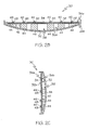
- FIGS. 2A , 2B and 2C depict a curved capacitive touch panel for an audio component according to a first embodiment of this invention.
- FIG. 2A is a front view of the touch panel
- FIG. 2B is a cross-sectional view along lines (2B-2B) of FIG. 2A
- FIG. 2C is a cross-sectional view along lines (2C-2C) of FIG. 2A .
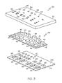
- FIG. 3 is an exploded isometric view of the curved capacitive touch panel of FIGS. 2A-2C .
- FIG. 4 is an exploded isometric view of curved capacitive touch panel for an audio component according to a second embodiment of this invention.
- FIGS. 1A and 1B illustrate a planar implementation of a capacitive sensing element 10 for a touch panel application.
- the sensing element or node is defined by a pair of conductive plates formed on the surface of a circuit board 12, one plate being defined by a small rectangular conductor 14, and the other being defined by a ground plane conductor 16 that surrounds but does not touch the small conductor 14.
- a detection circuit (not shown) is responsive to the electrical capacitance between the conductors 14 and 16, and detects a change in capacitance that occurs when a human finger 18 comes in proximity to the sensing element 10.
- FIGS. 1A-1B assumes the use of a planar trimplate 26
- styling considerations sometimes require the use of a non-planar trimplate having a curved touch surface 24.
- This of course results in a variable length air gap between the touch surface 24 and the planar array of capacitive sensing elements 10, and consequent problems with detection reliability.
- This problem is addressed according to the present invention by interposing a suitably sculpted high relative static permittivity material between the touch panel and the planar array of capacitive sensing elements.
- FIGS. 2A-2C and 3 A first embodiment of the invention is depicted in FIGS. 2A-2C and 3
- a second embodiment is depicted in FIG. 4 .
- the reference numeral 30 generally designates a capacitive touch panel for an automotive or consumer electronic product such as an audio system.
- the panel 30 includes a curved trimplate 32, a populated circuit board 34, and a silicone interface element 36.
- the trimplate 32 is constructed of a translucent material, the outboard face of which is painted and then selectively laser-etched to form an array of graphic indicia 38 that designate user touch points for selecting various audio functions.
- the circuit board 34 is mounted behind the trimplate 32 and, as best seen in FIG. 3 , supports an array of capacitive sensing nodes 40 in alignment with the graphic indicia 38 on trimplate 32.
- the silicone interface element 36 disposed between the circuit board 34 and trimplate 32, includes a planar base 42 that uniformly contacts the inboard face of circuit board 34, and a set of integral towers or pedestals 44 that extend toward and uniformly contact the inboard face 32a of trimplate 32.
- each touch point on the exposed face of trimplate 32 is coupled by a silicone tower 44 to a capacitive sensing node formed on circuit board 34.
- the respective silicone tower 44 provides a high relative static permittivity for concentrating the electrostatic lines of flux between each touch point and a respective capacitive sensing node.
- the capacitive sensing nodes reliably detect finger touches at the various touch points even though the distances between the circuit board 34 and the touch points vary substantially due to the trimplate curvature. Additionally, the silicone interface element 36 is compliant so that by gently compressing the interface element 36 between the trimplate 32 and sensing elements 40 eliminates any air gaps between the contacting surfaces.
- the silicone interface element 36 conducts light, allowing the graphic indicia 38 to be backlit by an array of LEDs 46 mounted on circuit board 34.
- the LEDs 46 are mounted on the outboard face 34a of circuit board 34 as shown in FIGS. 2B-2C , opposite respective circuit board openings 48 that direct the emitted light into the respective silicone towers 44. Mounting the LEDs 46 on the outboard face 34a of circuit board 34 preserves the planarity of the inboard face 34b so that the base 42 of silicone interface element 36 fully and uniformly engages the inboard face 34b for optimal coupling between the touch points on trimplate 32 and the corresponding capacitive sensing nodes 40 formed on circuit board 34.
- the silicone towers 44 not only conduct, but also diffuse, the light emitted by the LEDs 46, so no other light-modifying filters or lenses are needed.
- FIG. 4 depicts another capacitive touch panel 50 for an automotive or consumer electronic product such as an audio system, including a trimplate 52, a silicone interface element 54 and a planar circuit board 56.
- the trimplate 52 incorporates a set of three finger guides 58, 60, 62 with graphic indicia (not shown), openings 64, 66 for receiving a pair of knobs 68, 70, and a lens 72 through which a user views a display 74.
- the circuit board 56 supports the display 74, potentiometers 76, 78 for receiving the knobs 68, 70, and an array of capacitive sensing nodes aligned with the finger guides 58, 60, 62.
- the capacitive sensing nodes are not explicitly depicted in FIG.
- the silicone interface element 54 corresponds in outline to the three finger guides 58, 60, 62, and like the embodiment of FIGS. 2A-2C and 3 , includes a planar base 82 that uniformly contacts the circuit board 56, and a set of towers 84 extending from base 82 toward the trimplate 52. Also, the ends of the towers 84 are sculpted to match the inboard face of the trimplate 52 so that they uniformly contact the trimplate surface when the touch panel 50 is assembled.
- the towers 84 are relatively extensive in width, and are effectively subdivided by the recesses 86 to define a single tower for each of the touch points on finger guides 58, 60, 62.
- the recesses 86 also provide pathways to channel away any air trapped between the towers 84 and the inboard face of trimplate 52.
- the embodiment of FIG. 4 illustrates both an alternate construction of the silicone interface element, and a circuit board 56 that supports other elements (display 74 and potentiometers 76, 78) in addition to the array of capacitive sensing nodes.
- the present invention provides an improved and low-cost way of producing a capacitive touch panel having a non-planar touch surface through the use of a silicone interface element that propagates static electric fields between the non-planar touch surface and a planar capacitive sensor array. While the present invention has been described with respect to the illustrated embodiment, it is recognized that numerous modifications and variations in addition to those mentioned herein will occur to those skilled in the art. For example, the invention can be used with any number of sensing elements, and so forth. Accordingly, it is intended that the invention not be limited to the disclosed embodiment, but that it have the full scope permitted by the language of the following claims.
Landscapes
- Engineering & Computer Science (AREA)
- General Engineering & Computer Science (AREA)
- Theoretical Computer Science (AREA)
- Human Computer Interaction (AREA)
- Physics & Mathematics (AREA)
- General Physics & Mathematics (AREA)
- Switches That Are Operated By Magnetic Or Electric Fields (AREA)
- Position Input By Displaying (AREA)
- Casting Or Compression Moulding Of Plastics Or The Like (AREA)
Abstract
Description
- The present invention relates to a touch panel including a capacitive proximity sensor that detects a finger touch on the panel based on a change in the sensor's fringing capacitance, and more particularly to touch panel having a non-planar touch surface.
- Touch panels utilizing projected capacitance to detect a person's finger touch have been employed as a user interface in many consumer electronic products. The touch surface is the outboard face of a trimplate constructed of a dielectric material such as glass or plastic, and a capacitive sensor having an array of sensing nodes is located behind the trimplate. Each sensing node essentially comprises a pair of closely spaced conductive plates that are maintained at different electric potentials to establish a fringing electric field between them. When the user's finger touches the trimplate opposite a sensing node, the intensity of the fringing electric field changes due to capacitive coupling between the finger and each of the conductive plates, and a circuit detects the finger touch as a change in capacitance between the conductive plates.
- For best results, the distance between the touch surface and the array of capacitive sensing nodes should be substantially constant. This can be achieved at relatively low cost by using a planar trimplate and forming the sensing nodes, detection circuitry and other electronics on a planar circuit board that is mounted parallel to trimplate. In some cases, however, styling considerations require the use of a non-planar trimplate having a curved touch surface, resulting in undesired variation in distance between the touch surface and the sensing nodes formed on the planar circuit board. The usual approach in such cases is to form the sensing nodes on a flexible film and laminate the flexible film to the inboard face of the trimplate. This approach can be used effectively if the curvature is simple and gentle, but still results in higher overall cost because a separate circuit board must be provided for the detection circuitry, displays and so forth. And if the curvature of the trimplate is complex and/or severe, it becomes increasingly difficult to reliably laminate a flexible sensing film to its inboard face without incurring wrinkles and air pockets. Accordingly, what is needed is an improved and low-cost way of producing a capacitive touch panel having a non-planar touch surface.
- The present invention is directed to an improved capacitive touch panel including a trimplate defining a non-planar touch surface, a planar array of capacitive sensing elements mounted behind the trimplate, and a formable interface element of high relative static permittivity sandwiched between the sensing elements and the inboard face of the trimplate. Preferably, the interface element is a compression molded silicone rubber element having a first major surface that is sculpted to match and uniformly contact the inboard face of the trimplate, and a second major surface that is planar for uniformly contacting the planar array of capacitive sensing elements. The interface element may also have a limited amount of compliance so that mildly compressing the interface element between the trimplate and sensing elements eliminates any air gaps between the contacting surfaces.
-
FIGS. 1A and 1B conceptually depict a capacitive sensing element formed on a planar circuit board.FIG. 1A is a cross-sectional view, andFIG. 1B is a top view. -
FIGS. 2A ,2B and 2C depict a curved capacitive touch panel for an audio component according to a first embodiment of this invention.FIG. 2A is a front view of the touch panel,FIG. 2B is a cross-sectional view along lines (2B-2B) ofFIG. 2A , andFIG. 2C is a cross-sectional view along lines (2C-2C) ofFIG. 2A . -
FIG. 3 is an exploded isometric view of the curved capacitive touch panel ofFIGS. 2A-2C . -
FIG. 4 is an exploded isometric view of curved capacitive touch panel for an audio component according to a second embodiment of this invention. -
FIGS. 1A and 1B illustrate a planar implementation of acapacitive sensing element 10 for a touch panel application. In the illustrated configuration, the sensing element or node is defined by a pair of conductive plates formed on the surface of acircuit board 12, one plate being defined by a smallrectangular conductor 14, and the other being defined by aground plane conductor 16 that surrounds but does not touch thesmall conductor 14. A detection circuit (not shown) is responsive to the electrical capacitance between theconductors human finger 18 comes in proximity to thesensing element 10. In general, there is a direct capacitance betweenconductors electric field lines 20, and a fringing capacitance associated with the fringingelectric field lines 22. The capacitances are in parallel so that the measured capacitance is effectively their sum. Whenfinger 18 touches thesurface 24 of adielectric trimplate 26, the fringing capacitances are altered due to capacitive coupling between thefinger 18 and theconductors - While the illustration of
FIGS. 1A-1B assumes the use of aplanar trimplate 26, styling considerations sometimes require the use of a non-planar trimplate having acurved touch surface 24. This of course results in a variable length air gap between thetouch surface 24 and the planar array ofcapacitive sensing elements 10, and consequent problems with detection reliability. This problem is addressed according to the present invention by interposing a suitably sculpted high relative static permittivity material between the touch panel and the planar array of capacitive sensing elements. A first embodiment of the invention is depicted inFIGS. 2A-2C and3 , and a second embodiment is depicted inFIG. 4 . - Referring to
FIGS. 2A-2C and3 , thereference numeral 30 generally designates a capacitive touch panel for an automotive or consumer electronic product such as an audio system. Thepanel 30 includes acurved trimplate 32, a populatedcircuit board 34, and asilicone interface element 36. Thetrimplate 32 is constructed of a translucent material, the outboard face of which is painted and then selectively laser-etched to form an array ofgraphic indicia 38 that designate user touch points for selecting various audio functions. Thecircuit board 34 is mounted behind thetrimplate 32 and, as best seen inFIG. 3 , supports an array ofcapacitive sensing nodes 40 in alignment with thegraphic indicia 38 ontrimplate 32. Thesilicone interface element 36, disposed between thecircuit board 34 andtrimplate 32, includes aplanar base 42 that uniformly contacts the inboard face ofcircuit board 34, and a set of integral towers orpedestals 44 that extend toward and uniformly contact theinboard face 32a oftrimplate 32. - The ends of the
silicone towers 44 are contoured to match the local curvature of thetrimplate 32 as shown so that thetowers 44 fully and uniformly contact theinboard face 32a oftrimplate 32 with only a small amount of force biasing thetrimplate 32 toward the circuit board 34 (which force may be provided simply by mounting thecircuit board 34 in the audio component). Thus, each touch point on the exposed face oftrimplate 32 is coupled by asilicone tower 44 to a capacitive sensing node formed oncircuit board 34. For each touch point, therespective silicone tower 44 provides a high relative static permittivity for concentrating the electrostatic lines of flux between each touch point and a respective capacitive sensing node. As a result, the capacitive sensing nodes reliably detect finger touches at the various touch points even though the distances between thecircuit board 34 and the touch points vary substantially due to the trimplate curvature. Additionally, thesilicone interface element 36 is compliant so that by gently compressing theinterface element 36 between thetrimplate 32 and sensingelements 40 eliminates any air gaps between the contacting surfaces. - Another advantageous aspect of the
silicone interface element 36 is that it conducts light, allowing thegraphic indicia 38 to be backlit by an array ofLEDs 46 mounted oncircuit board 34. In the illustrated embodiment, theLEDs 46 are mounted on theoutboard face 34a ofcircuit board 34 as shown inFIGS. 2B-2C , opposite respectivecircuit board openings 48 that direct the emitted light into therespective silicone towers 44. Mounting theLEDs 46 on theoutboard face 34a ofcircuit board 34 preserves the planarity of theinboard face 34b so that thebase 42 ofsilicone interface element 36 fully and uniformly engages theinboard face 34b for optimal coupling between the touch points ontrimplate 32 and the correspondingcapacitive sensing nodes 40 formed oncircuit board 34. Thesilicone towers 44 not only conduct, but also diffuse, the light emitted by theLEDs 46, so no other light-modifying filters or lenses are needed. -
FIG. 4 depicts anothercapacitive touch panel 50 for an automotive or consumer electronic product such as an audio system, including atrimplate 52, a silicone interface element 54 and aplanar circuit board 56. In this case, thetrimplate 52 incorporates a set of three finger guides 58, 60, 62 with graphic indicia (not shown),openings knobs lens 72 through which a user views adisplay 74. Thecircuit board 56 supports thedisplay 74,potentiometers knobs FIG. 4 , but their locations are identified by theopenings 80 that pass light emitted from an array of rear-mounted LEDs (not shown). The silicone interface element 54 corresponds in outline to the three finger guides 58, 60, 62, and like the embodiment ofFIGS. 2A-2C and3 , includes aplanar base 82 that uniformly contacts thecircuit board 56, and a set oftowers 84 extending frombase 82 toward thetrimplate 52. Also, the ends of thetowers 84 are sculpted to match the inboard face of thetrimplate 52 so that they uniformly contact the trimplate surface when thetouch panel 50 is assembled. In this case, however, thetowers 84 are relatively extensive in width, and are effectively subdivided by therecesses 86 to define a single tower for each of the touch points on finger guides 58, 60, 62. Advantageously, therecesses 86 also provide pathways to channel away any air trapped between thetowers 84 and the inboard face oftrimplate 52. Thus, relative to the embodiment ofFIGS. 2A-2C and3 , the embodiment ofFIG. 4 illustrates both an alternate construction of the silicone interface element, and acircuit board 56 that supports other elements (display 74 andpotentiometers 76, 78) in addition to the array of capacitive sensing nodes. - In summary, the present invention provides an improved and low-cost way of producing a capacitive touch panel having a non-planar touch surface through the use of a silicone interface element that propagates static electric fields between the non-planar touch surface and a planar capacitive sensor array. While the present invention has been described with respect to the illustrated embodiment, it is recognized that numerous modifications and variations in addition to those mentioned herein will occur to those skilled in the art. For example, the invention can be used with any number of sensing elements, and so forth. Accordingly, it is intended that the invention not be limited to the disclosed embodiment, but that it have the full scope permitted by the language of the following claims.
Claims (7)
- A capacitive touch panel (10/50), comprising:a planar circuit board (34/56) supporting an array of capacitive sensing elements (40);a trimplate (32/52) spaced apart from said planar circuit board (34/56), and defining a non-planar touch surface (24) with an array of touch points (38) in alignment with the array of capacitive sensing elements (40), the various touch points (38) being separated from respective capacitive sensing elements (40) by different distances due to the non-planarity of the touch surface (24) and the planarity of the circuit board (34/56); anda silicone interface element (36/54) sandwiched between said planar circuit board (34/56) and said trimplate (32/52) for electrically coupling the touch points (38) to the respective capacitive sensing elements (40) to compensate for the different distances.
- The capacitive touch panel of claim 1, where:said silicone interface element (36/54) includes a planar base (42/82) that uniformly contacts an inboard face (34b) of said planar circuit board (34/56), and an array of towers (44/84) that extend from said planar base (42/82) and uniformly contact an inboard face (32a) of said trimplate (32/52) in alignment with said array of touch points (38).
- The capacitive touch panel of claim 2, where:the towers (44/84) of said silicone interface element (36/54) have ends that are sculpted to match and uniformly contact the inboard face (32a) of said trimplate (32/52).
- The capacitive touch panel of claim 2, where:said touch points (38) and the towers (44/84) of said silicone interface element (36/54) are both light transmissive; andsaid circuit board (34/56) supports an array of light emitting devices (46) that direct light through said towers (44/84) and said touch points (38) to backlight said touch points (38).
- The capacitive touch panel of claim 4, where:said light emitting devices (46) are mounted on an outboard face (34a) of said circuit board (34/56) to preserve the planarity of said inboard face (34b); andsaid circuit board (34/56) includes openings (48) that pass light emitted by said light emitting devices (46) into said towers (44/84) and said touch points (38).
- The capacitive touch panel of claim 2, where:said array of towers (84) are defined by recesses (86) formed in a block of silicone material that extends from said base (82).
- The capacitive touch panel of claim 1, where:said silicone interface element (36/54) is characterized by both compliance and a high relative static permittivity.
Applications Claiming Priority (1)
| Application Number | Priority Date | Filing Date | Title |
|---|---|---|---|
| US12/474,295 US20100302200A1 (en) | 2009-05-29 | 2009-05-29 | Capacitive touch panel having a non-planar touch surface |
Publications (2)
| Publication Number | Publication Date |
|---|---|
| EP2256602A2 true EP2256602A2 (en) | 2010-12-01 |
| EP2256602A3 EP2256602A3 (en) | 2013-10-02 |
Family
ID=42664874
Family Applications (1)
| Application Number | Title | Priority Date | Filing Date |
|---|---|---|---|
| EP10162604.2A Withdrawn EP2256602A3 (en) | 2009-05-29 | 2010-05-11 | Capacitive touch panel having a non-planar touch surface |
Country Status (2)
| Country | Link |
|---|---|
| US (1) | US20100302200A1 (en) |
| EP (1) | EP2256602A3 (en) |
Cited By (2)
| Publication number | Priority date | Publication date | Assignee | Title |
|---|---|---|---|---|
| DE102016213868A1 (en) * | 2016-07-28 | 2018-02-01 | Bayerische Motoren Werke Aktiengesellschaft | Touch input device and electronic system for a motor vehicle and motor vehicle |
| WO2018091152A1 (en) * | 2016-11-15 | 2018-05-24 | Volkswagen Aktiengesellschaft | Device having a touch-sensitive free-form surface and method for the production thereof |
Families Citing this family (34)
| Publication number | Priority date | Publication date | Assignee | Title |
|---|---|---|---|---|
| KR101471801B1 (en) | 2009-08-21 | 2014-12-10 | 애플 인크. | Methods and apparatus for capacitive sensing |
| US8928336B2 (en) | 2011-06-09 | 2015-01-06 | Ford Global Technologies, Llc | Proximity switch having sensitivity control and method therefor |
| US9143126B2 (en) | 2011-09-22 | 2015-09-22 | Ford Global Technologies, Llc | Proximity switch having lockout control for controlling movable panel |
| US10112556B2 (en) | 2011-11-03 | 2018-10-30 | Ford Global Technologies, Llc | Proximity switch having wrong touch adaptive learning and method |
| US8994228B2 (en) | 2011-11-03 | 2015-03-31 | Ford Global Technologies, Llc | Proximity switch having wrong touch feedback |
| US8878438B2 (en) | 2011-11-04 | 2014-11-04 | Ford Global Technologies, Llc | Lamp and proximity switch assembly and method |
| US9520875B2 (en) | 2012-04-11 | 2016-12-13 | Ford Global Technologies, Llc | Pliable proximity switch assembly and activation method |
| US9944237B2 (en) | 2012-04-11 | 2018-04-17 | Ford Global Technologies, Llc | Proximity switch assembly with signal drift rejection and method |
| US8933708B2 (en) | 2012-04-11 | 2015-01-13 | Ford Global Technologies, Llc | Proximity switch assembly and activation method with exploration mode |
| US9568527B2 (en) | 2012-04-11 | 2017-02-14 | Ford Global Technologies, Llc | Proximity switch assembly and activation method having virtual button mode |
| US9831870B2 (en) | 2012-04-11 | 2017-11-28 | Ford Global Technologies, Llc | Proximity switch assembly and method of tuning same |
| US9065447B2 (en) | 2012-04-11 | 2015-06-23 | Ford Global Technologies, Llc | Proximity switch assembly and method having adaptive time delay |
| US9660644B2 (en) | 2012-04-11 | 2017-05-23 | Ford Global Technologies, Llc | Proximity switch assembly and activation method |
| US9559688B2 (en) | 2012-04-11 | 2017-01-31 | Ford Global Technologies, Llc | Proximity switch assembly having pliable surface and depression |
| US9531379B2 (en) | 2012-04-11 | 2016-12-27 | Ford Global Technologies, Llc | Proximity switch assembly having groove between adjacent proximity sensors |
| US9184745B2 (en) * | 2012-04-11 | 2015-11-10 | Ford Global Technologies, Llc | Proximity switch assembly and method of sensing user input based on signal rate of change |
| US9287864B2 (en) | 2012-04-11 | 2016-03-15 | Ford Global Technologies, Llc | Proximity switch assembly and calibration method therefor |
| US9197206B2 (en) | 2012-04-11 | 2015-11-24 | Ford Global Technologies, Llc | Proximity switch having differential contact surface |
| US9219472B2 (en) | 2012-04-11 | 2015-12-22 | Ford Global Technologies, Llc | Proximity switch assembly and activation method using rate monitoring |
| US9136840B2 (en) | 2012-05-17 | 2015-09-15 | Ford Global Technologies, Llc | Proximity switch assembly having dynamic tuned threshold |
| US8981602B2 (en) | 2012-05-29 | 2015-03-17 | Ford Global Technologies, Llc | Proximity switch assembly having non-switch contact and method |
| US9337832B2 (en) | 2012-06-06 | 2016-05-10 | Ford Global Technologies, Llc | Proximity switch and method of adjusting sensitivity therefor |
| US9641172B2 (en) | 2012-06-27 | 2017-05-02 | Ford Global Technologies, Llc | Proximity switch assembly having varying size electrode fingers |
| US8922340B2 (en) | 2012-09-11 | 2014-12-30 | Ford Global Technologies, Llc | Proximity switch based door latch release |
| US8796575B2 (en) | 2012-10-31 | 2014-08-05 | Ford Global Technologies, Llc | Proximity switch assembly having ground layer |
| US9311204B2 (en) | 2013-03-13 | 2016-04-12 | Ford Global Technologies, Llc | Proximity interface development system having replicator and method |
| JP6166635B2 (en) * | 2013-10-03 | 2017-07-19 | ダイキョーニシカワ株式会社 | Switch device for vehicle |
| US10038443B2 (en) | 2014-10-20 | 2018-07-31 | Ford Global Technologies, Llc | Directional proximity switch assembly |
| US9654103B2 (en) | 2015-03-18 | 2017-05-16 | Ford Global Technologies, Llc | Proximity switch assembly having haptic feedback and method |
| US9548733B2 (en) | 2015-05-20 | 2017-01-17 | Ford Global Technologies, Llc | Proximity sensor assembly having interleaved electrode configuration |
| CN110140098B (en) | 2016-07-11 | 2023-08-11 | 上海延锋金桥汽车饰件系统有限公司 | vehicle interior parts |
| JP7341146B2 (en) * | 2018-08-24 | 2023-09-08 | シャープ株式会社 | Air cleaner |
| WO2021011536A1 (en) | 2019-07-15 | 2021-01-21 | Shanghai Yanfeng Jinqiao Automotive Trim Systems Co. Ltd. | Vehicle interior component |
| CN110768653B (en) * | 2019-09-29 | 2024-01-19 | 福州丹诺西诚电子科技有限公司 | Touch sensing structure of automobile touch switch |
Family Cites Families (8)
| Publication number | Priority date | Publication date | Assignee | Title |
|---|---|---|---|---|
| DE102004060846B4 (en) * | 2004-12-17 | 2008-12-18 | Diehl Ako Stiftung & Co. Kg | Capacitive touch switch |
| WO2007099733A1 (en) * | 2006-03-01 | 2007-09-07 | Sharp Kabushiki Kaisha | Input device using touch panel |
| US20070229470A1 (en) * | 2006-03-31 | 2007-10-04 | Warren Snyder | Capacitive touch sense device having polygonal shaped sensor elements |
| KR101225973B1 (en) * | 2006-06-09 | 2013-01-24 | 엘지전자 주식회사 | Capacitance type switch of electric and electronic device |
| US20080309633A1 (en) * | 2007-06-13 | 2008-12-18 | Apple Inc. | Touch-sensitive display |
| US20100066683A1 (en) * | 2008-09-17 | 2010-03-18 | Shih-Chang Chang | Method for Transferring Thin Film to Substrate |
| TW201013495A (en) * | 2008-09-30 | 2010-04-01 | Hannstar Display Corp | In-cell capacitive type sensing input display device |
| TWI385567B (en) * | 2008-12-30 | 2013-02-11 | Univ Nat Chiao Tung | Capacitive touch panel |
-
2009
- 2009-05-29 US US12/474,295 patent/US20100302200A1/en not_active Abandoned
-
2010
- 2010-05-11 EP EP10162604.2A patent/EP2256602A3/en not_active Withdrawn
Non-Patent Citations (1)
| Title |
|---|
| None |
Cited By (4)
| Publication number | Priority date | Publication date | Assignee | Title |
|---|---|---|---|---|
| DE102016213868A1 (en) * | 2016-07-28 | 2018-02-01 | Bayerische Motoren Werke Aktiengesellschaft | Touch input device and electronic system for a motor vehicle and motor vehicle |
| US11126309B2 (en) | 2016-07-28 | 2021-09-21 | Bayerische Motoren Werke Aktiengesellschaft | Touch input device and electronic system for a motor vehicle, and motor vehicle |
| WO2018091152A1 (en) * | 2016-11-15 | 2018-05-24 | Volkswagen Aktiengesellschaft | Device having a touch-sensitive free-form surface and method for the production thereof |
| US10938391B2 (en) | 2016-11-15 | 2021-03-02 | Volkswagen Aktiengesellschaft | Device having a touch-sensitive free-form surface and method for the production thereof |
Also Published As
| Publication number | Publication date |
|---|---|
| EP2256602A3 (en) | 2013-10-02 |
| US20100302200A1 (en) | 2010-12-02 |
Similar Documents
| Publication | Publication Date | Title |
|---|---|---|
| EP2256602A2 (en) | Capacitive touch panel having a non-planar touch surface | |
| KR101033154B1 (en) | Touch panel | |
| KR101712346B1 (en) | Touch input device | |
| CN105717682B (en) | Touch display device | |
| KR101565822B1 (en) | Smartphone | |
| US20070291963A1 (en) | Input device | |
| TWI382158B (en) | Electrostatic Capacitive Sensors | |
| KR101410175B1 (en) | Portable communication device having touch key | |
| US20150301640A1 (en) | Input device, display device, and electronic apparatus | |
| CN105075121B (en) | Operating unit for coffee machine | |
| US10324555B2 (en) | Display device having force sensor structure | |
| CN102043554A (en) | Electrostatic capacitive touch panel input device | |
| KR20160076298A (en) | Touch input device | |
| KR20140135478A (en) | Fingerprint sensor module for mobile device and manufacturing methode thereof | |
| KR20160034240A (en) | Smartphone | |
| US10528164B2 (en) | Display device, backlight unit, guide panel, and flexible printed circuit | |
| CN113095250A (en) | Touch display module and under-screen fingerprint identification module thereof | |
| CN103345316A (en) | Electronic device with touch control function | |
| KR101857080B1 (en) | Electrode sheet and touch input device | |
| EP3721559B1 (en) | Backlit user interface | |
| CN113095245A (en) | Touch display module and fingerprint identification module under screen thereof | |
| KR101734989B1 (en) | Touch input device | |
| US10883889B2 (en) | Display device including a pressure sensor with an opening in the electrode | |
| CN105867538B (en) | Electronic equipment | |
| KR20180052580A (en) | Electrode sheet and touch input device |
Legal Events
| Date | Code | Title | Description |
|---|---|---|---|
| PUAI | Public reference made under article 153(3) epc to a published international application that has entered the european phase |
Free format text: ORIGINAL CODE: 0009012 |
|
| AK | Designated contracting states |
Kind code of ref document: A2 Designated state(s): AL AT BE BG CH CY CZ DE DK EE ES FI FR GB GR HR HU IE IS IT LI LT LU LV MC MK MT NL NO PL PT RO SE SI SK SM TR |
|
| AX | Request for extension of the european patent |
Extension state: BA ME RS |
|
| PUAL | Search report despatched |
Free format text: ORIGINAL CODE: 0009013 |
|
| AK | Designated contracting states |
Kind code of ref document: A3 Designated state(s): AL AT BE BG CH CY CZ DE DK EE ES FI FR GB GR HR HU IE IS IT LI LT LU LV MC MK MT NL NO PL PT RO SE SI SK SM TR |
|
| AX | Request for extension of the european patent |
Extension state: BA ME RS |
|
| RIC1 | Information provided on ipc code assigned before grant |
Ipc: H03K 17/96 20060101AFI20130829BHEP Ipc: G06F 3/02 20060101ALI20130829BHEP |
|
| STAA | Information on the status of an ep patent application or granted ep patent |
Free format text: STATUS: THE APPLICATION IS DEEMED TO BE WITHDRAWN |
|
| 18D | Application deemed to be withdrawn |
Effective date: 20140403 |