EP2256829A1 - Herstellungsverfahren für eine Dünnfilm-Solarzelle und Dünnfilm-Solarzellenmodul - Google Patents
Herstellungsverfahren für eine Dünnfilm-Solarzelle und Dünnfilm-Solarzellenmodul Download PDFInfo
- Publication number
- EP2256829A1 EP2256829A1 EP09161300A EP09161300A EP2256829A1 EP 2256829 A1 EP2256829 A1 EP 2256829A1 EP 09161300 A EP09161300 A EP 09161300A EP 09161300 A EP09161300 A EP 09161300A EP 2256829 A1 EP2256829 A1 EP 2256829A1
- Authority
- EP
- European Patent Office
- Prior art keywords
- solar cell
- particles
- thin film
- dry cleaning
- manufacturing
- Prior art date
- Legal status (The legal status is an assumption and is not a legal conclusion. Google has not performed a legal analysis and makes no representation as to the accuracy of the status listed.)
- Granted
Links
Images



Classifications
-
- H—ELECTRICITY
- H10—SEMICONDUCTOR DEVICES; ELECTRIC SOLID-STATE DEVICES NOT OTHERWISE PROVIDED FOR
- H10F—INORGANIC SEMICONDUCTOR DEVICES SENSITIVE TO INFRARED RADIATION, LIGHT, ELECTROMAGNETIC RADIATION OF SHORTER WAVELENGTH OR CORPUSCULAR RADIATION
- H10F71/00—Manufacture or treatment of devices covered by this subclass
- H10F71/138—Manufacture of transparent electrodes, e.g. transparent conductive oxides [TCO] or indium tin oxide [ITO] electrodes
-
- H—ELECTRICITY
- H10—SEMICONDUCTOR DEVICES; ELECTRIC SOLID-STATE DEVICES NOT OTHERWISE PROVIDED FOR
- H10F—INORGANIC SEMICONDUCTOR DEVICES SENSITIVE TO INFRARED RADIATION, LIGHT, ELECTROMAGNETIC RADIATION OF SHORTER WAVELENGTH OR CORPUSCULAR RADIATION
- H10F77/00—Constructional details of devices covered by this subclass
- H10F77/10—Semiconductor bodies
- H10F77/16—Material structures, e.g. crystalline structures, film structures or crystal plane orientations
- H10F77/169—Thin semiconductor films on metallic or insulating substrates
-
- H—ELECTRICITY
- H10—SEMICONDUCTOR DEVICES; ELECTRIC SOLID-STATE DEVICES NOT OTHERWISE PROVIDED FOR
- H10F—INORGANIC SEMICONDUCTOR DEVICES SENSITIVE TO INFRARED RADIATION, LIGHT, ELECTROMAGNETIC RADIATION OF SHORTER WAVELENGTH OR CORPUSCULAR RADIATION
- H10F77/00—Constructional details of devices covered by this subclass
- H10F77/20—Electrodes
- H10F77/206—Electrodes for devices having potential barriers
- H10F77/211—Electrodes for devices having potential barriers for photovoltaic cells
-
- H—ELECTRICITY
- H10—SEMICONDUCTOR DEVICES; ELECTRIC SOLID-STATE DEVICES NOT OTHERWISE PROVIDED FOR
- H10P—GENERIC PROCESSES OR APPARATUS FOR THE MANUFACTURE OR TREATMENT OF DEVICES COVERED BY CLASS H10
- H10P72/00—Handling or holding of wafers, substrates or devices during manufacture or treatment thereof
- H10P72/04—Apparatus for manufacture or treatment
- H10P72/0402—Apparatus for fluid treatment
- H10P72/0406—Apparatus for fluid treatment for cleaning followed by drying, rinsing, stripping, blasting or the like
-
- Y—GENERAL TAGGING OF NEW TECHNOLOGICAL DEVELOPMENTS; GENERAL TAGGING OF CROSS-SECTIONAL TECHNOLOGIES SPANNING OVER SEVERAL SECTIONS OF THE IPC; TECHNICAL SUBJECTS COVERED BY FORMER USPC CROSS-REFERENCE ART COLLECTIONS [XRACs] AND DIGESTS
- Y02—TECHNOLOGIES OR APPLICATIONS FOR MITIGATION OR ADAPTATION AGAINST CLIMATE CHANGE
- Y02E—REDUCTION OF GREENHOUSE GAS [GHG] EMISSIONS, RELATED TO ENERGY GENERATION, TRANSMISSION OR DISTRIBUTION
- Y02E10/00—Energy generation through renewable energy sources
- Y02E10/50—Photovoltaic [PV] energy
Definitions
- the present embodiment relates to a manufacturing method of a thin film solar cell and a thin film solar cell module.
- a solar cell is a semiconductor device converting solar energy into electrical energy.
- the solar cell may be classified into a silicon type, a chemical compound type, and an organic material type according to its material.
- a silicon system solar cell is classified into a single crystalline silicon solar cell, a polycrystalline silicon solar cell, and an amorphous silicon solar cell according to a phase of a semiconductor.
- the solar cell is classified into a bulk (substrate) type solar cell and a thin film type solar cell according to a thickness of a semiconductor.
- the thin film type solar cell has a semiconductor layer with a thickness of less than several tens of ⁇ m or several ⁇ m.
- a single crystalline silicon solar cell and a polycrystalline silicon solar cell of the silicon system solar cell belong to a bulk type.
- An amorphous silicon solar cell belongs to a thin film type.
- the chemical compound solar cell is classified into a bulk type consisting of Group III-V Gallium Arsenide (GaAs) and Group III-V Indium Phosphide (InP), and a thin-film type consisting of Group II-VI Cadmium Telluride (CdTe) and Group I-III-VI Copper Indium Diselenide (CIS; CulnSe2).
- the organic material solar cell is largely divided into an organic molecule type and organic/inorganic combination type. Besides these a dye-sensitized solar cell belongs to a thin-film type.
- the transparent electrode is made of a low iron tempered glass, an indium tin oxide (ITO), or a tin oxide (SnO 2 ).
- a lightweight flexible substrate of low cost such as polyimide, polyethylen terephthalate (PET), PEN, aluminum (Al) foil, or stainless steel can be used.
- a transparent electrode When a substrate is contaminated with an organic material, a transparent electrode is readily peeled off from the substrate during formation of the solar cell, and the organic substances are diffused into an absorber layer, thereby reducing photo-electric conversion efficiency of the solar cell.
- particles occurring during a unit process can be conveyed to other substrates through a conveyor or a robot in an in-line mass production line.
- particles can form pin holes.
- conductive particles remain in a laser-patterning line, they may block insulation between adjacent unit cells to reduce yield and efficiency of a solar cell module.
- a pure water cleaner using alkali detergent for cleaning is widely used to remove organic substances and particles formed on a surface of the substrate.
- a pure water cleaner is widely used to perform cleaning for removing particles formed on a surface of the substrate during patterning.
- the resultant object is patterned in a laser patterning process.
- a metal electrode formed on the semiconductor layer is patterned, thereby constructing an internally serial-interconnected solar cell.
- a cleaning process can be instantly performed by a pure water cleaner.
- a solar cell module is manufactured through works such as formation of a bus bar and assembling a module.
- edge insulation is achieved.
- Al aluminum
- an edge exclusion process is carried out prior to formation of the bus bar.
- the edge exclusion process removes semiconductor and conductive thin films formed on edge regions of the substrate to a predetermined width.
- cleaning is performed using a pure water cleaner.
- the pure water cleaner is composed of a unit sufficiently flowing pure water or detergent mixing water on a surface, a roll brush unit, a pure water rinsing unit, and an air knife unit removing moisture, a length of equipment is long to increase a total area of a mass production line of a solar cell.
- a manufacturing method of a thin film solar cell comprises performing dry cleaning of an insulation substrate on which a transparent electrode is formed, patterning the transparent electrodes to be spaced apart from each other, performing dry cleaning of the patterned transparent electrodes, forming a semiconductor layer on surfaces of the transparent electrodes and patterning a metal electrode on the semiconductor layer.
- the step of performing the dry cleaning of the insulation substrate may include removing an organic material and removing particles.
- Ozone may be used when the organic material is removed, and the ozone may be produced using one of atmosphere pressure plasma, a ultra-violet lamp, or a combination of the atmosphere pressure plasma and the ultra-violet lamp.
- the step of removing the particles may include floating particles on the insulation substrate using cooling dried air and sucking the particles.
- the step of performing the dry cleaning of the patterned transparent electrodes may include floating particles on the patterned transparent electrodes and sucking the floated particles in a circumference.
- the manufacturing method may further comprise performing a dry cleaning of the patterned metal electrode.
- the step of performing the dry cleaning of the patterned metal electrode may include floating particles on the metal electrode and sucking the floated particles.
- the organic material may be removed by ozone after removal of the particles.
- Nitrogen gas in plasma atmosphere may be used in the step of performing the dry cleaning of the patterned transparent electrode.
- FIG. 1 is a cross-sectional view illustrating a structure of a thin film solar cell manufactured by manufacturing methods of a thin film solar cell and a thin film solar cell module in accordance with a first embodiment
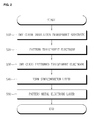
- FIG. 2 is a flow chart illustrating a manufacturing method of a thin film solar cell in accordance with a second embodiment
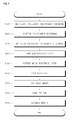
- FIG. 3 is a flow chart illustrating a manufacturing method of a thin film solar cell in accordance with a third embodiment
- FIG. 4 is a flow chart illustrating a manufacturing method of a thin film solar cell module in accordance with a fourth embodiment.
- FIG. 5 is a flow chart illustrating a manufacturing method of a thin film solar cell module in accordance with a fifth embodiment.
- a thin film solar cell 1 has a structure in which a plurality of unit cells 20 are electrically interconnected in series on a transparent substrate 10 such as a glass substrate or a transparent plastic substrate.
- the thin film solar cell 1 includes band shaped transparent electrodes 22 on a transparent substrate 10 being an insulator to be insulated each other, a band shaped unit semiconductor layer 24 covering the transparent electrode 22, and a band shaped metal electrode layer 26 covering the semiconductor layer 24.
- a plurality of unit cells 20 are electrically interconnected in series on the transparent substrate 10.
- a rear passivation layer 30 covers the metal electrode layer 26.
- the rear passivation layer 30 is made of resin.
- the laser patterning method etches the transparent electrode 22, the semiconductor layer 24, the metal electrode layer 26, and the like using YAG laser beam.
- the semiconductor layer 24 and the metal electrode layer 26 are sequentially deposited on the transparent electrode 22.
- the resultant object is covered by a rear passivation layer 30 to manufacture the thin film solar cell 1.
- the transparent substrate 10 is contaminated with an organic substance or particles are produced during a unit process, the yield and efficiency of a solar cell module can be deteriorated.
- initial cleaning, patterned transparent electrode cleaning, patterned metal electrode cleaning, and cleaning after edge exclusion are performed in a dry cleaning.
- Each of manufacturing methods of a thin film solar cell in accordance with the present embodiments include: patterning a transparent electrode 22 formed on an insulation transparent substrate 10 (S20), forming a semiconductor layer 24 on a surface of the transparent electrode 22 (S40), and patterning a metal electrode layer 26 on the semiconductor layer 24 (S50).
- a manufacturing method of a thin film solar cell in accordance with a second embodiment includes: performing a dry cleaning of the insulation transparent substrate 10 with nitrogen (N 2 ) of low purity and cooling dried air (CDA) before the transparent electrode 20 is formed on the insulation transparent substrate 10 (S10); patterning the transparent electrode 22 (S20), and performing a dry cleaning of the patterned transparent electrode 22 (S30) subsequent to step S20.
- N 2 nitrogen
- CDA cooling dried air
- a cleaning method using one of atmosphere pressure plasma, Eximer Ultra-Violet (EUV), or an Ultra Sonic Cleaner (USC) may be used as the dry cleaning method.
- nitrogen of low purity and CDA are used.
- the nitrogen of low purity has about 2N purity as plasma atmosphere gas.
- the CDA is reaction gas.
- An O radical is produced by plasma and reacts with oxygen (O 2 ) in atmosphere to produce ozone.
- the ozone reacts with an organic material to output CO and CO 2 .
- the CO and CO 2 are discharged such that the organic material is removed.
- the cleaning method using the EUV produces ozone in atmosphere using an excimer laser as a ultra-violet light source.
- the ozone reacts with an organic material to produce volatile CO/CO 2 , which is then discharged. Consequently, the organic material is removed.
- a blow unit blows the CDA to the transparent substrate 10 with a constant time period (frequency). Accordingly, when an ultrasonic wave is generated and particles on the transparent substrate 10 float, a suction head sucks the floated particles with the result that a pre-filter collects the particles.
- a dry cleaning system includes a unit removing the organic material by using nitrogen (N 2 ) of low purity and CDA, and a unit removing the particles by using CDA. Accordingly, in the manufacturing method of the present embodiment, the transparent substrate 10 is conveyed by driving a horizontal conveyor, and a procedure removing the organic material and a procedure removing the particles can be performed.
- the unit removing the organic material removes the organic material using one of atmosphere pressure plasma, ultra-violet (UV) lamp, or a combination of the atmosphere pressure plasma and the ultra-violet (UV) lamp.
- the atmosphere pressure plasma and the ultra-violet (UV) lamp generates ozone in atmosphere to remove the organic material on a surface of the transparent substrate 10.
- a particle removal unit positioned at a rear portion can include a suction head blowing the particles on the transparent substrate 10 to suck the particles.
- a suction head blowing the particles on the transparent substrate 10 to suck the particles.
- a zinc oxide (ZnO) thin film is used as the transparent electrode 22, electron mobility of the zinc oxide (ZnO) thin film is increased by ozone processing to thereby reduce resistivity as an additional advantage.
- dry cleaning may be achieved through USC. Accordingly, after the transparent electrode 22 is patterned by a laser patterning device, generated particles are removed.
- the transparent substrate 10 is conveyed by driving a horizontal conveyer, and particles on the transparent substrate 10 float through CDA.
- the suction head sucks to remove the particles.
- electric energy and CDA as necessary utilities, and general exhaustion is required.
- an ultra-violet lamp can be installed at a rear part of the particle removal device. Consequently, after removal of the particles, the organic material can be removed by ozone.
- an ozone exhaust device can be provided. The ozone can be removed by the ozone exhaust device.
- the organic material or the particles deposited on the insulation transparent substrate 10 or the transparent substrate 10 coated with the transparent electrode 22 are removed by dry cleaning, and the transparent electrode 22, the semiconductor layer 24 and the metal electrode layer 26 are sequentially deposited.
- a manufacturing method of a thin film solar cell in accordance with a third embodiment includes: performing a dry cleaning of the insulation transparent substrate 10 (S10) with nitrogen (N 2 ) of low purity and cooling dried air prior to patterning the transparent electrode 22 (S20), performing a dry cleaning of the patterned transparent electrode 22 with CDA subsequent to step S20 (S30), and performing a dry cleaning of a patterned metal electrode layer with CDA (S60) subsequent to a step of patterning the metal electrode layer 26 (S50).
- steps S10 to S50 of the third embodiment were described in the second embodiment, an explanation thereof will be omitted.
- a dry cleaning step S60 of the metal electrode layer 26 is performed to remove particles produced during pattern formation of the metal electrode layer after the pattern formation thereof. So as to remove the particles, the foregoing USC method can be used.
- the manufacturing method of a thin film solar cell includes a dry cleaning step before or after patterning the transparent electrode 22 formed on the insulation transparent substrate 10.
- the manufacturing method of the present invention can further include dry cleaning step of a transparent substrate 10 on which a transparent electrode 22 is patterned.
- embodiments of a manufacturing method of a thin film solar cell module each include patterning transparent electrodes on an insulation transparent substrate 10 to be spaced apart from each other by a predetermined distance (S200), forming a semiconductor layer 24 on surfaces of the transparent electrodes 22 (S400), patterning a metal electrode layer 26 on the semiconductor layer 24 (S500), and removing parts of the transparent electrodes 22, the semiconductor layer 24, and the metal electrode layer 26 formed on edges of the transparent substrate 10 to a predetermined width (S600).
- a manufacturing method of a thin film solar cell module in accordance with a fourth embodiment includes: performing a dry cleaning of an insulation transparent substrate 10 with nitrogen (N 2 ) of low purity and CDA (S100), patterning a transparent electrode 22 (S200), performing a dry cleaning of the patterned transparent electrode 22 with the CDA (S300), an edge exclusion step (S600), and performing a dry cleaning of edges with the CDA (S700).
- steps S100, S200, and S300 of FIG. 4 are identical with steps S10, S20, and S30 of FIG. 2 , a detailed description thereof will be omitted.
- a thin film solar cell is constructed in a method shown in FIGS. 1 and 2 , edges of the thin film solar cell are excluded (S600), and a solar cell module is manufactured through a bus bar formation step (S800) and a module assembling step (S900).
- an edge exclusion step (S600) removing a semiconductor layer 24 and conductive thin films formed on edge parts of a transparent substrate 10 to a predetermined width is carried out prior to the bus bar formation (S800).
- a dry cleaning (S700) is performed to clean plural particles produced in the edge exclusion step (S600).
- the transparent substrate 10 is conveyed by driving a horizontal conveyer, and CDA blows particles on the transparent substrate 10 by an USC method, then a suction head sucks the particles in the vicinity of the transparent substrate 10, thereby removing the particles.
- CDA blows particles on the transparent substrate 10 by an USC method
- a suction head sucks the particles in the vicinity of the transparent substrate 10, thereby removing the particles.
- electric energy and CDA as necessary utilities, and a general exhaust process is required.
- a manufacturing method of a thin film solar cell module in accordance with a fifth embodiment includes: performing a dry cleaning of an insulation transparent substrate 10 with nitrogen (N 2 ) of low purity and CDA (S100), patterning the transparent electrode 22 (S200), performing a dry cleaning of the patterned transparent electrode 22 with CDA (S300), patterning a metal electrode layer 26 (S500), performing a dry cleaning of the patterned metal electrode layer 26 with CDA (S550), an edge exclusion step (S600), and dry cleaning edges with CDA (S700).
- Manufacturing methods of a thin film solar cell and a thin film solar cell module in accordance with the present embodiments perform dry cleaning using a dry cleaning unit in place of a pure water cleaner. Namely, because the length of the pure water cleaner is long, an occupied area of the pure water cleaner is relatively large in a total solar cell mass production line. Further, in a case of the pure water cleaner, maintenance costs are increased and a large amount of waste water is generated in the production of a large amount of pure water and to manage resistance greater than a predetermined value. In contrast, in a case of a dry cleaning unit, initial manufacturing costs and running costs may be reduced in a thin film solar cell and module mass production line.
Landscapes
- Photovoltaic Devices (AREA)
Priority Applications (1)
| Application Number | Priority Date | Filing Date | Title |
|---|---|---|---|
| EP09161300A EP2256829B1 (de) | 2009-05-27 | 2009-05-27 | Herstellungsverfahren für eine Dünnfilm-Solarzelle und Dünnfilm-Solarzellenmodul |
Applications Claiming Priority (1)
| Application Number | Priority Date | Filing Date | Title |
|---|---|---|---|
| EP09161300A EP2256829B1 (de) | 2009-05-27 | 2009-05-27 | Herstellungsverfahren für eine Dünnfilm-Solarzelle und Dünnfilm-Solarzellenmodul |
Publications (2)
| Publication Number | Publication Date |
|---|---|
| EP2256829A1 true EP2256829A1 (de) | 2010-12-01 |
| EP2256829B1 EP2256829B1 (de) | 2012-06-06 |
Family
ID=42314799
Family Applications (1)
| Application Number | Title | Priority Date | Filing Date |
|---|---|---|---|
| EP09161300A Not-in-force EP2256829B1 (de) | 2009-05-27 | 2009-05-27 | Herstellungsverfahren für eine Dünnfilm-Solarzelle und Dünnfilm-Solarzellenmodul |
Country Status (1)
| Country | Link |
|---|---|
| EP (1) | EP2256829B1 (de) |
Citations (8)
| Publication number | Priority date | Publication date | Assignee | Title |
|---|---|---|---|---|
| US4393267A (en) * | 1981-05-26 | 1983-07-12 | Chevron Research Company | Method for improving the efficiency of a solar cell and an improved cadmium sulfide/copper sulfide photovoltaic cell |
| DE19516446A1 (de) * | 1995-05-04 | 1996-11-07 | Siemens Solar Gmbh | Verfahren zur Herstellung eines Dünnschichthalbleiterbauelements über einer TCO-Elektrodenschicht |
| US6240931B1 (en) * | 1996-11-05 | 2001-06-05 | Ebara Corporation | Method for removing particles from a surface of an article |
| US20020170586A1 (en) * | 2001-03-28 | 2002-11-21 | Lee Moon-Hee | Method of and apparatus for removing contaminants from surface of a substrate |
| US20030037457A1 (en) * | 2001-08-27 | 2003-02-27 | Applied Materials, Inc. | Particle removal apparatus |
| US20030168660A1 (en) * | 2002-03-05 | 2003-09-11 | Sanyo Electric Co., Ltd. | Photovoltaic device and manufacturing method thereof |
| US20060096622A1 (en) * | 2004-11-11 | 2006-05-11 | Samsung Electronics Co., Ltd. | Dry cleaning apparatus used to manufacture semiconductor devices |
| US20080223434A1 (en) * | 2007-02-19 | 2008-09-18 | Showa Denko K.K. | Solar cell and process for producing the same |
-
2009
- 2009-05-27 EP EP09161300A patent/EP2256829B1/de not_active Not-in-force
Patent Citations (8)
| Publication number | Priority date | Publication date | Assignee | Title |
|---|---|---|---|---|
| US4393267A (en) * | 1981-05-26 | 1983-07-12 | Chevron Research Company | Method for improving the efficiency of a solar cell and an improved cadmium sulfide/copper sulfide photovoltaic cell |
| DE19516446A1 (de) * | 1995-05-04 | 1996-11-07 | Siemens Solar Gmbh | Verfahren zur Herstellung eines Dünnschichthalbleiterbauelements über einer TCO-Elektrodenschicht |
| US6240931B1 (en) * | 1996-11-05 | 2001-06-05 | Ebara Corporation | Method for removing particles from a surface of an article |
| US20020170586A1 (en) * | 2001-03-28 | 2002-11-21 | Lee Moon-Hee | Method of and apparatus for removing contaminants from surface of a substrate |
| US20030037457A1 (en) * | 2001-08-27 | 2003-02-27 | Applied Materials, Inc. | Particle removal apparatus |
| US20030168660A1 (en) * | 2002-03-05 | 2003-09-11 | Sanyo Electric Co., Ltd. | Photovoltaic device and manufacturing method thereof |
| US20060096622A1 (en) * | 2004-11-11 | 2006-05-11 | Samsung Electronics Co., Ltd. | Dry cleaning apparatus used to manufacture semiconductor devices |
| US20080223434A1 (en) * | 2007-02-19 | 2008-09-18 | Showa Denko K.K. | Solar cell and process for producing the same |
Non-Patent Citations (3)
| Title |
|---|
| DAVIS ET AL: "Properties of transparent conducting oxides deposited at room temperature", THIN SOLID FILMS, ELSEVIER-SEQUOIA S.A. LAUSANNE, CH LNKD- DOI:10.1016/0040-6090(93)90632-Y, vol. 236, no. 1-2, 15 December 1993 (1993-12-15), pages 1 - 5, XP025732535, ISSN: 0040-6090, [retrieved on 19931215] * |
| HANABUSA M ET AL: "Pulsed laser deposition of silicon films for solar cell applications", NUCLEAR INSTRUMENTS & METHODS IN PHYSICS RESEARCH, SECTION - B:BEAM INTERACTIONS WITH MATERIALS AND ATOMS, ELSEVIER, AMSTERDAM, NL LNKD- DOI:10.1016/S0168-583X(96)00539-3, vol. 121, no. 1, 1 January 1997 (1997-01-01), pages 367 - 370, XP004057943, ISSN: 0168-583X * |
| VIG J R: "UV/ozone cleaning of surfaces", JOURNAL OF VACUUM SCIENCE & TECHNOLOGY A (VACUUM, SURFACES, AND FILMS) USA, vol. 3, no. 3, May 1985 (1985-05-01), pages 1027 - 1034, XP002592914, ISSN: 0734-2101 * |
Also Published As
| Publication number | Publication date |
|---|---|
| EP2256829B1 (de) | 2012-06-06 |
Similar Documents
| Publication | Publication Date | Title |
|---|---|---|
| US5131954A (en) | Monolithic solar cell array and method for its manufacturing | |
| KR101028971B1 (ko) | 집적형 박막 태양전지 및 그의 제조 방법 | |
| EP2249395A1 (de) | Dünnschicht-solarbatterie und verfahren zu ihrer herstellung | |
| US20060112987A1 (en) | Transparent thin-film solar cell module and its manufacturing method | |
| US7906365B2 (en) | Method of manufacturing solar cell panel | |
| CN102084500B (zh) | 用于光伏器件的装配线 | |
| KR101070199B1 (ko) | 박막형 태양전지 및 그 제조방법 | |
| JP5230627B2 (ja) | 光電変換装置およびその製造方法 | |
| CN101622719B (zh) | 光电变换装置及其制造方法 | |
| EP3001461A1 (de) | Solarzelle, solarzellenmodul, verfahren zur herstellung einer solarzelle und verfahren zur herstellung eines solarzellenmoduls | |
| CN112909128A (zh) | 异质结太阳能电池片的制造方法及异质结太阳能电池片 | |
| US20100323471A1 (en) | Selective Etch of Laser Scribed Solar Cell Substrate | |
| AU2018403240A1 (en) | Method of manufacturing shingled solar modules | |
| CN113471337A (zh) | 异质结太阳能电池片的制备方法 | |
| US7939444B2 (en) | Manufacturing methods of thin film solar cell and thin film solar cell module | |
| CN101779294B (zh) | 光电转换装置 | |
| KR100901745B1 (ko) | 박막 태양전지 및 모듈 제조방법 | |
| EP2256829B1 (de) | Herstellungsverfahren für eine Dünnfilm-Solarzelle und Dünnfilm-Solarzellenmodul | |
| KR101000383B1 (ko) | 집적형 박막 태양전지 및 그 제조 방법 | |
| JP2004119953A (ja) | 薄膜太陽電池およびその製造方法 | |
| JP2004214565A (ja) | 集積型薄膜太陽電池の製造方法および集積型薄膜太陽電池 | |
| CN102460698A (zh) | 用于制造薄膜光伏转换器设备的方法 | |
| KR101649850B1 (ko) | 태양전지와 그 제조방법 및 태양전지 제조용 식각장비 | |
| EP0962990A2 (de) | Herstellungsverfahren von Solarzellen | |
| JPH11330513A (ja) | 集積型シリコン系薄膜光電変換装置の製造方法 |
Legal Events
| Date | Code | Title | Description |
|---|---|---|---|
| PUAI | Public reference made under article 153(3) epc to a published international application that has entered the european phase |
Free format text: ORIGINAL CODE: 0009012 |
|
| 17P | Request for examination filed |
Effective date: 20090527 |
|
| AK | Designated contracting states |
Kind code of ref document: A1 Designated state(s): AT BE BG CH CY CZ DE DK EE ES FI FR GB GR HR HU IE IS IT LI LT LU LV MC MK MT NL NO PL PT RO SE SI SK TR |
|
| RIC1 | Information provided on ipc code assigned before grant |
Ipc: H01L 31/0224 20060101ALI20110920BHEP Ipc: H01L 27/142 20060101ALI20110920BHEP Ipc: H01L 31/18 20060101AFI20110920BHEP |
|
| GRAP | Despatch of communication of intention to grant a patent |
Free format text: ORIGINAL CODE: EPIDOSNIGR1 |
|
| GRAS | Grant fee paid |
Free format text: ORIGINAL CODE: EPIDOSNIGR3 |
|
| GRAA | (expected) grant |
Free format text: ORIGINAL CODE: 0009210 |
|
| AK | Designated contracting states |
Kind code of ref document: B1 Designated state(s): AT BE BG CH CY CZ DE DK EE ES FI FR GB GR HR HU IE IS IT LI LT LU LV MC MK MT NL NO PL PT RO SE SI SK TR |
|
| REG | Reference to a national code |
Ref country code: GB Ref legal event code: FG4D |
|
| REG | Reference to a national code |
Ref country code: AT Ref legal event code: REF Ref document number: 561396 Country of ref document: AT Kind code of ref document: T Effective date: 20120615 Ref country code: CH Ref legal event code: EP |
|
| REG | Reference to a national code |
Ref country code: IE Ref legal event code: FG4D |
|
| REG | Reference to a national code |
Ref country code: DE Ref legal event code: R096 Ref document number: 602009007433 Country of ref document: DE Effective date: 20120802 |
|
| REG | Reference to a national code |
Ref country code: NL Ref legal event code: VDEP Effective date: 20120606 |
|
| PG25 | Lapsed in a contracting state [announced via postgrant information from national office to epo] |
Ref country code: LT Free format text: LAPSE BECAUSE OF FAILURE TO SUBMIT A TRANSLATION OF THE DESCRIPTION OR TO PAY THE FEE WITHIN THE PRESCRIBED TIME-LIMIT Effective date: 20120606 Ref country code: NO Free format text: LAPSE BECAUSE OF FAILURE TO SUBMIT A TRANSLATION OF THE DESCRIPTION OR TO PAY THE FEE WITHIN THE PRESCRIBED TIME-LIMIT Effective date: 20120906 Ref country code: CY Free format text: LAPSE BECAUSE OF FAILURE TO SUBMIT A TRANSLATION OF THE DESCRIPTION OR TO PAY THE FEE WITHIN THE PRESCRIBED TIME-LIMIT Effective date: 20120606 Ref country code: FI Free format text: LAPSE BECAUSE OF FAILURE TO SUBMIT A TRANSLATION OF THE DESCRIPTION OR TO PAY THE FEE WITHIN THE PRESCRIBED TIME-LIMIT Effective date: 20120606 Ref country code: SE Free format text: LAPSE BECAUSE OF FAILURE TO SUBMIT A TRANSLATION OF THE DESCRIPTION OR TO PAY THE FEE WITHIN THE PRESCRIBED TIME-LIMIT Effective date: 20120606 |
|
| REG | Reference to a national code |
Ref country code: AT Ref legal event code: MK05 Ref document number: 561396 Country of ref document: AT Kind code of ref document: T Effective date: 20120606 |
|
| REG | Reference to a national code |
Ref country code: LT Ref legal event code: MG4D Effective date: 20120606 |
|
| PG25 | Lapsed in a contracting state [announced via postgrant information from national office to epo] |
Ref country code: LV Free format text: LAPSE BECAUSE OF FAILURE TO SUBMIT A TRANSLATION OF THE DESCRIPTION OR TO PAY THE FEE WITHIN THE PRESCRIBED TIME-LIMIT Effective date: 20120606 Ref country code: SI Free format text: LAPSE BECAUSE OF FAILURE TO SUBMIT A TRANSLATION OF THE DESCRIPTION OR TO PAY THE FEE WITHIN THE PRESCRIBED TIME-LIMIT Effective date: 20120606 Ref country code: HR Free format text: LAPSE BECAUSE OF FAILURE TO SUBMIT A TRANSLATION OF THE DESCRIPTION OR TO PAY THE FEE WITHIN THE PRESCRIBED TIME-LIMIT Effective date: 20120606 Ref country code: GR Free format text: LAPSE BECAUSE OF FAILURE TO SUBMIT A TRANSLATION OF THE DESCRIPTION OR TO PAY THE FEE WITHIN THE PRESCRIBED TIME-LIMIT Effective date: 20120907 |
|
| PG25 | Lapsed in a contracting state [announced via postgrant information from national office to epo] |
Ref country code: NL Free format text: LAPSE BECAUSE OF FAILURE TO SUBMIT A TRANSLATION OF THE DESCRIPTION OR TO PAY THE FEE WITHIN THE PRESCRIBED TIME-LIMIT Effective date: 20120606 Ref country code: AT Free format text: LAPSE BECAUSE OF FAILURE TO SUBMIT A TRANSLATION OF THE DESCRIPTION OR TO PAY THE FEE WITHIN THE PRESCRIBED TIME-LIMIT Effective date: 20120606 Ref country code: EE Free format text: LAPSE BECAUSE OF FAILURE TO SUBMIT A TRANSLATION OF THE DESCRIPTION OR TO PAY THE FEE WITHIN THE PRESCRIBED TIME-LIMIT Effective date: 20120606 Ref country code: SK Free format text: LAPSE BECAUSE OF FAILURE TO SUBMIT A TRANSLATION OF THE DESCRIPTION OR TO PAY THE FEE WITHIN THE PRESCRIBED TIME-LIMIT Effective date: 20120606 Ref country code: CZ Free format text: LAPSE BECAUSE OF FAILURE TO SUBMIT A TRANSLATION OF THE DESCRIPTION OR TO PAY THE FEE WITHIN THE PRESCRIBED TIME-LIMIT Effective date: 20120606 Ref country code: RO Free format text: LAPSE BECAUSE OF FAILURE TO SUBMIT A TRANSLATION OF THE DESCRIPTION OR TO PAY THE FEE WITHIN THE PRESCRIBED TIME-LIMIT Effective date: 20120606 Ref country code: IS Free format text: LAPSE BECAUSE OF FAILURE TO SUBMIT A TRANSLATION OF THE DESCRIPTION OR TO PAY THE FEE WITHIN THE PRESCRIBED TIME-LIMIT Effective date: 20121006 Ref country code: BE Free format text: LAPSE BECAUSE OF FAILURE TO SUBMIT A TRANSLATION OF THE DESCRIPTION OR TO PAY THE FEE WITHIN THE PRESCRIBED TIME-LIMIT Effective date: 20120606 |
|
| PG25 | Lapsed in a contracting state [announced via postgrant information from national office to epo] |
Ref country code: PL Free format text: LAPSE BECAUSE OF FAILURE TO SUBMIT A TRANSLATION OF THE DESCRIPTION OR TO PAY THE FEE WITHIN THE PRESCRIBED TIME-LIMIT Effective date: 20120606 Ref country code: PT Free format text: LAPSE BECAUSE OF FAILURE TO SUBMIT A TRANSLATION OF THE DESCRIPTION OR TO PAY THE FEE WITHIN THE PRESCRIBED TIME-LIMIT Effective date: 20121008 Ref country code: IT Free format text: LAPSE BECAUSE OF FAILURE TO SUBMIT A TRANSLATION OF THE DESCRIPTION OR TO PAY THE FEE WITHIN THE PRESCRIBED TIME-LIMIT Effective date: 20120606 |
|
| PLBE | No opposition filed within time limit |
Free format text: ORIGINAL CODE: 0009261 |
|
| STAA | Information on the status of an ep patent application or granted ep patent |
Free format text: STATUS: NO OPPOSITION FILED WITHIN TIME LIMIT |
|
| PG25 | Lapsed in a contracting state [announced via postgrant information from national office to epo] |
Ref country code: ES Free format text: LAPSE BECAUSE OF FAILURE TO SUBMIT A TRANSLATION OF THE DESCRIPTION OR TO PAY THE FEE WITHIN THE PRESCRIBED TIME-LIMIT Effective date: 20120917 Ref country code: DK Free format text: LAPSE BECAUSE OF FAILURE TO SUBMIT A TRANSLATION OF THE DESCRIPTION OR TO PAY THE FEE WITHIN THE PRESCRIBED TIME-LIMIT Effective date: 20120606 |
|
| 26N | No opposition filed |
Effective date: 20130307 |
|
| REG | Reference to a national code |
Ref country code: DE Ref legal event code: R097 Ref document number: 602009007433 Country of ref document: DE Effective date: 20130307 |
|
| PG25 | Lapsed in a contracting state [announced via postgrant information from national office to epo] |
Ref country code: BG Free format text: LAPSE BECAUSE OF FAILURE TO SUBMIT A TRANSLATION OF THE DESCRIPTION OR TO PAY THE FEE WITHIN THE PRESCRIBED TIME-LIMIT Effective date: 20120906 |
|
| REG | Reference to a national code |
Ref country code: DE Ref legal event code: R082 Ref document number: 602009007433 Country of ref document: DE Representative=s name: PATRONUS IP PATENT- & RECHTSANWAELTE BERNHARD , DE |
|
| PG25 | Lapsed in a contracting state [announced via postgrant information from national office to epo] |
Ref country code: MC Free format text: LAPSE BECAUSE OF FAILURE TO SUBMIT A TRANSLATION OF THE DESCRIPTION OR TO PAY THE FEE WITHIN THE PRESCRIBED TIME-LIMIT Effective date: 20120606 |
|
| REG | Reference to a national code |
Ref country code: CH Ref legal event code: PL |
|
| GBPC | Gb: european patent ceased through non-payment of renewal fee |
Effective date: 20130527 |
|
| PG25 | Lapsed in a contracting state [announced via postgrant information from national office to epo] |
Ref country code: DE Free format text: LAPSE BECAUSE OF NON-PAYMENT OF DUE FEES Effective date: 20131203 Ref country code: LI Free format text: LAPSE BECAUSE OF NON-PAYMENT OF DUE FEES Effective date: 20130531 Ref country code: CH Free format text: LAPSE BECAUSE OF NON-PAYMENT OF DUE FEES Effective date: 20130531 |
|
| REG | Reference to a national code |
Ref country code: IE Ref legal event code: MM4A |
|
| REG | Reference to a national code |
Ref country code: DE Ref legal event code: R119 Ref document number: 602009007433 Country of ref document: DE Effective date: 20131203 |
|
| REG | Reference to a national code |
Ref country code: FR Ref legal event code: ST Effective date: 20140131 |
|
| PG25 | Lapsed in a contracting state [announced via postgrant information from national office to epo] |
Ref country code: GB Free format text: LAPSE BECAUSE OF NON-PAYMENT OF DUE FEES Effective date: 20130527 Ref country code: IE Free format text: LAPSE BECAUSE OF NON-PAYMENT OF DUE FEES Effective date: 20130527 |
|
| PG25 | Lapsed in a contracting state [announced via postgrant information from national office to epo] |
Ref country code: FR Free format text: LAPSE BECAUSE OF NON-PAYMENT OF DUE FEES Effective date: 20130531 |
|
| PG25 | Lapsed in a contracting state [announced via postgrant information from national office to epo] |
Ref country code: MT Free format text: LAPSE BECAUSE OF FAILURE TO SUBMIT A TRANSLATION OF THE DESCRIPTION OR TO PAY THE FEE WITHIN THE PRESCRIBED TIME-LIMIT Effective date: 20120606 |
|
| PG25 | Lapsed in a contracting state [announced via postgrant information from national office to epo] |
Ref country code: TR Free format text: LAPSE BECAUSE OF FAILURE TO SUBMIT A TRANSLATION OF THE DESCRIPTION OR TO PAY THE FEE WITHIN THE PRESCRIBED TIME-LIMIT Effective date: 20120606 |
|
| PG25 | Lapsed in a contracting state [announced via postgrant information from national office to epo] |
Ref country code: MK Free format text: LAPSE BECAUSE OF FAILURE TO SUBMIT A TRANSLATION OF THE DESCRIPTION OR TO PAY THE FEE WITHIN THE PRESCRIBED TIME-LIMIT Effective date: 20120606 Ref country code: LU Free format text: LAPSE BECAUSE OF NON-PAYMENT OF DUE FEES Effective date: 20130527 Ref country code: HU Free format text: LAPSE BECAUSE OF FAILURE TO SUBMIT A TRANSLATION OF THE DESCRIPTION OR TO PAY THE FEE WITHIN THE PRESCRIBED TIME-LIMIT; INVALID AB INITIO Effective date: 20090527 |