EP2256836A2 - Élément multicouche et procédé de son fabrication - Google Patents
Élément multicouche et procédé de son fabrication Download PDFInfo
- Publication number
- EP2256836A2 EP2256836A2 EP10179362A EP10179362A EP2256836A2 EP 2256836 A2 EP2256836 A2 EP 2256836A2 EP 10179362 A EP10179362 A EP 10179362A EP 10179362 A EP10179362 A EP 10179362A EP 2256836 A2 EP2256836 A2 EP 2256836A2
- Authority
- EP
- European Patent Office
- Prior art keywords
- inner electrode
- multilayer
- holes
- multilayer component
- ceramic
- Prior art date
- Legal status (The legal status is an assumption and is not a legal conclusion. Google has not performed a legal analysis and makes no representation as to the accuracy of the status listed.)
- Granted
Links
Images

Classifications
-
- H—ELECTRICITY
- H10—SEMICONDUCTOR DEVICES; ELECTRIC SOLID-STATE DEVICES NOT OTHERWISE PROVIDED FOR
- H10N—ELECTRIC SOLID-STATE DEVICES NOT OTHERWISE PROVIDED FOR
- H10N30/00—Piezoelectric or electrostrictive devices
- H10N30/01—Manufacture or treatment
- H10N30/05—Manufacture of multilayered piezoelectric or electrostrictive devices, or parts thereof, e.g. by stacking piezoelectric bodies and electrodes
- H10N30/053—Manufacture of multilayered piezoelectric or electrostrictive devices, or parts thereof, e.g. by stacking piezoelectric bodies and electrodes by integrally sintering piezoelectric or electrostrictive bodies and electrodes
-
- H—ELECTRICITY
- H10—SEMICONDUCTOR DEVICES; ELECTRIC SOLID-STATE DEVICES NOT OTHERWISE PROVIDED FOR
- H10N—ELECTRIC SOLID-STATE DEVICES NOT OTHERWISE PROVIDED FOR
- H10N30/00—Piezoelectric or electrostrictive devices
- H10N30/01—Manufacture or treatment
- H10N30/06—Forming electrodes or interconnections, e.g. leads or terminals
- H10N30/067—Forming single-layered electrodes of multilayered piezoelectric or electrostrictive parts
-
- H—ELECTRICITY
- H10—SEMICONDUCTOR DEVICES; ELECTRIC SOLID-STATE DEVICES NOT OTHERWISE PROVIDED FOR
- H10N—ELECTRIC SOLID-STATE DEVICES NOT OTHERWISE PROVIDED FOR
- H10N30/00—Piezoelectric or electrostrictive devices
- H10N30/80—Constructional details
- H10N30/87—Electrodes or interconnections, e.g. leads or terminals
- H10N30/871—Single-layered electrodes of multilayer piezoelectric or electrostrictive devices, e.g. internal electrodes
-
- Y—GENERAL TAGGING OF NEW TECHNOLOGICAL DEVELOPMENTS; GENERAL TAGGING OF CROSS-SECTIONAL TECHNOLOGIES SPANNING OVER SEVERAL SECTIONS OF THE IPC; TECHNICAL SUBJECTS COVERED BY FORMER USPC CROSS-REFERENCE ART COLLECTIONS [XRACs] AND DIGESTS
- Y10—TECHNICAL SUBJECTS COVERED BY FORMER USPC
- Y10T—TECHNICAL SUBJECTS COVERED BY FORMER US CLASSIFICATION
- Y10T29/00—Metal working
- Y10T29/42—Piezoelectric device making
Definitions
- the present invention relates to a multilayer component and to a method for its production.
- a key role for the application of multilayer components comprising piezoelectric and ferroelectric actuators is played by the mechanical inherent rigidity of the component.
- Piezoceramic materials based on lead zirconate titanate are known.
- lead zirconate titanate having a perovskite structure A 2+ B 4 + O 3 a desired stabilization of the materials is achieved by partial substitution with ferroelectrically active compounds, while at the same time allowing the reduction of the sintering temperature.
- An object to be solved is to specify a multilayer component which achieves a high deflection path with the lowest possible voltage.
- a multilayer component which comprises the following features: a ceramic base body and at least one inner electrode arranged in the ceramic base body, the inner electrode having a plurality of holes.
- Such a multilayer component has the advantage that the rigidity of the inner electrode against a transverse axial contraction is partially or completely reduced and thereby a quasi interference-free transverse axial transverse contraction of the inner electrode is possible during an axial deflection of the multilayer component. With the transverse contraction, a higher axial deflection path of the multilayer component is simultaneously achieved with the same applied voltage.
- the multilayer component can advantageously be densely sintered, since an inner electrode provided with a plurality of holes provides a lower mechanical resistance to the ceramic of the base body, which always strives to shrink during sintering.
- a higher sintering density is accompanied by improved electrical properties, and is thus advantageous.
- a higher sintering density also allows a higher deflection path. Depending on the application, this can be of particular advantage for a piezoelectric actuator.
- ceramic films be provided on which inner electrode material, preferably in the form of a paste, is printed.
- the films are stacked, cut or first cut and then stacked.
- the multilayer component thus obtained is then sintered.
- a silver-palladium mixture wherein preferably silver is present in a weight fraction of between 60 and 80% and palladium in a weight fraction of between 20 and 40%.
- a paste is formed, which is printed on the ceramic films to be stacked. That so
- the component obtained is sintered at a temperature between 1120 and 1220 ° C, preferably at 1170 ° C, wherein the internal electrode material softens just enough during the sintering process to form a reticular structure.
- an internal electrode material is used whose liquidus temperature is so slightly different from the sintering temperature of the ceramic base body that the ceramic base body is sintered and at the same time the internal electrode forms a plurality of holes. This results in the advantage that small holes can be produced in the inner electrode layer. In this case, the electromagnetic field distribution of the inner electrode is more homogeneous, the smaller the holes of the inner electrode are formed.
- the internal electrode material copper or a copper alloy may be used.
- the material is screen-printed onto the ceramic sheets in the form of a paste, using a screen which preferably results in a printed pattern of the inner electrode having holes with diameters between 10 and 20 ⁇ m. After stacking the films, the resulting device is sintered at a temperature between 1000 ° C and 1100 ° C, preferably at 1050 ° C, sintered.
- the stiffness of multilayer actuators was measured for testing purposes, for example on a force or displacement measuring station.
- the integral component stiffness value resulting from the measurement was attributed one to one to the elasticity of the ceramic.
- a higher stiffness index indicated a harder ceramic, depending on whether the ceramic was donor-doped or acceptor doped. Based on this consideration, it was above all the composition of the ceramic (ceramic formulation) that sought to set the modulus of elasticity of the multilayer piezoactuator and thus the component rigidity.
- the multilayer component comprises a multilayer piezoactuator, wherein other multilayer components are also possible, such as multilayer capacitors or other multilayer ceramic devices.
- piezo / ferroelectric materials It is a characteristic of piezo / ferroelectric materials to deflect when voltage is applied. With the deflection in a spatial direction, for example the axial direction (lower arrow), a transverse axial contraction (upper arrow) or transverse contraction in the spatial directions is normal to the deflection direction. In multilayer piezoelectric actuators with continuous internal electrodes, this transverse contraction opposes the internal electrodes as mechanical counterparts and thereby reduces the transverse contraction and thus also the deflection of the component in comparison to a monolithic ceramic cuboid without internal electrodes.
- the inner electrodes 2 are provided with holes, but it is not necessary for the holes to completely pierce the inner electrode - preferably they can also be realized as substantial indentations.
- the integral modulus of elasticity of the multilayer piezoelectric actuator and thus its stiffness can be varied for a given geometry.
- the degree of interruption 3D is shown as areas free of electrode material within the inner electrode.
- the thickness of the internal electrodes is kept as low as possible, since on the one hand smaller amounts of electrode material are used and thus lower costs incurred, and on the other hand, a higher sintering density of the multilayer component can be achieved.
- the multilayer piezoelectric actuator is preferably designed such that the internal electrodes are connected to an electrically conductive contact layer in order to produce the electrical connection to a voltage and current source.
- FIG. 2 illustrates the structure of an internal electrode 2 according to the invention.
- the white circles represent the holes 3.
- the degree of interruption is expressed as a percentage.
- An inner electrode 2 provided with holes can be produced with a suitable thermal process control of the maximum sintering temperature in relation to the liquidus temperature of the inner electrode material.
- the per se known liquidus temperature of the internal electrode material must be above the maximum Sintering temperature of the multilayer piezoelectric actuator are so that the inner electrode just softens when the maximum sintering temperature is reached.
- foils which contain ceramic material with piezoelectric properties, for example lead zirconate titanate.
- ceramic material with piezoelectric properties for example lead zirconate titanate.
- piezoelectrically active ceramic material which has a different composition, for example a mixture of lead zirconate titanate and lead nickel niobate and a material which does not contain lead, for example sodium potassium niobate.
- the films are printed by means of a screen printing process with a paste containing a mixture of silver and palladium in a ratio of preferably between 60 and 95 wt .-% silver and 5 to 40 wt .-% palladium for the preparation of the internal electrodes.
- a ratio of 70 to 30 parts by weight of the respective materials leads to particularly good results.
- an adjustment of the process temperature required for the production of the electrical component is possible in order to form, with different sintering temperatures, the reticular structure of the inner electrode 2, and at the same time to achieve sufficient sintering densification of the ceramic.
- a paste provided for screen printing on the ceramic sheets contains copper or a copper alloy.
- the screen is coated with a film in such a way as to produce a printing pattern in which the Copper layer is provided with circular interruptions or holes each having about 10 to 20 microns in diameter.
- the films printed with the silver palladium paste or with the copper or copper alloy paste are stacked and pressed together to form a stack corresponding to the function of the electrical component.
- the component containing the said mixture also contains silver and palladium as internal electrode is heated to a temperature of 1170 ° and held at this temperature for two hours. This temperature is below the mixing ratio-dependent liquidus temperature of the silver-palladium mixture, which is for a mixing ratio of 70% silver and 30% palladium at 1228 ° C.
- the ceramic is sintered, forming in the inner electrode, the desired network structure.
- the device containing copper or copper alloy as the inner electrode is heated to 1050 ° C after the organic binder is burned out and held at that temperature for two hours while being sintered.
- the reticular structure of the copper electrode is effected by the type of printing with a suitable sieve.
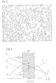
- FIG. 3 shows a SEM image of a net shape formed by the thermal process control inner electrode.
- the expected during sintering number of holes 3 and their accumulated surface can be determined by experience Test results are determined, wherein the formation of the holes of the temperature and the pressure during sintering and the material of the inner electrode is affected.
- FIG. 4 shows qualitatively a curve K, which represents the change in the rigidity of the inner electrode as a function of the degree of interruption UG.
- Curve V shows voltages applied to the multilayer piezoelectric actuator to achieve a given deflection path L of the multilayer piezoelectric actuator.
- the curve L shows different deflection paths, which are achieved with a constant voltage.
- the shape of the curves L and V is also dependent on the degree of interruption of the inner electrode or on its rigidity K. Since the curves V, K, and L all relate to different physical quantities, the left axis of the graph is given without a significant unit. It is particularly preferred that the inner electrode has a degree of interruption within that in the FIG.
- the diameters of the circular holes of the inner electrode are 10 ⁇ m to 15 ⁇ m and / or the areas of non-circular holes are about 50 to 90 ⁇ m 2 .
- These relatively small sizes prevent the holes from forming unwanted and interfering electric fields. With this measure, the electric field over the entire inner electrode considered homogeneous become. For such small holes, it is therefore advantageous to form the holes during sintering according to the manufacturing method according to the invention, since such small holes are difficult to realize by screen printing process.
- the sintered density of the ceramic base body or its dielectric or ceramic layers is related to the geometric structure of the inner electrode. If the internal electrodes are continuous, they provide greater resistance to the tendency of the ceramic body to shrink during sintering. Holes provided internal electrodes in contrast allow the production of multilayer devices with a tendency to higher sintering densities, since the internal electrodes oppose a lower resistance to shrinkage of the ceramic body. Higher sintering densities have the advantage that a greater grain growth accompanied by pore elimination, or reduction of free grain surfaces of the ceramic material is made possible, generally aiming at a reduction of the surface and grain boundary energy, which leads to a decrease in the total free energy of the sintered sintered body.
- the electrical properties of the sintered Krellpiezoaktors are thus improved because, for example, a more homogeneous electromagnetic field distribution and a simpler and predictable deflection behavior of Learntikpiezoaktors is ensured.
- a higher sintering density is therefore of particular interest not only for multilayer piezoactuators but, for example, also for multilayer capacitors.
Landscapes
- Engineering & Computer Science (AREA)
- Manufacturing & Machinery (AREA)
- General Electrical Machinery Utilizing Piezoelectricity, Electrostriction Or Magnetostriction (AREA)
- Fuel-Injection Apparatus (AREA)
- Ceramic Capacitors (AREA)
- Fixed Capacitors And Capacitor Manufacturing Machines (AREA)
Applications Claiming Priority (2)
| Application Number | Priority Date | Filing Date | Title |
|---|---|---|---|
| DE102004038103A DE102004038103A1 (de) | 2004-08-05 | 2004-08-05 | Vielschichtbauelement und Verfahren zu dessen Herstellung |
| EP05774389A EP1774603B1 (fr) | 2004-08-05 | 2005-08-05 | Dispositif multicouche et procede pour sa production |
Related Parent Applications (2)
| Application Number | Title | Priority Date | Filing Date |
|---|---|---|---|
| EP05774389.0 Division | 2005-08-05 | ||
| EP05774389A Division EP1774603B1 (fr) | 2004-08-05 | 2005-08-05 | Dispositif multicouche et procede pour sa production |
Publications (3)
| Publication Number | Publication Date |
|---|---|
| EP2256836A2 true EP2256836A2 (fr) | 2010-12-01 |
| EP2256836A3 EP2256836A3 (fr) | 2011-01-05 |
| EP2256836B1 EP2256836B1 (fr) | 2012-10-10 |
Family
ID=35044666
Family Applications (2)
| Application Number | Title | Priority Date | Filing Date |
|---|---|---|---|
| EP10179362A Ceased EP2256836B1 (fr) | 2004-08-05 | 2005-08-05 | Procédé de fabrication d'un élément multicouche |
| EP05774389A Ceased EP1774603B1 (fr) | 2004-08-05 | 2005-08-05 | Dispositif multicouche et procede pour sa production |
Family Applications After (1)
| Application Number | Title | Priority Date | Filing Date |
|---|---|---|---|
| EP05774389A Ceased EP1774603B1 (fr) | 2004-08-05 | 2005-08-05 | Dispositif multicouche et procede pour sa production |
Country Status (5)
| Country | Link |
|---|---|
| US (1) | US7692368B2 (fr) |
| EP (2) | EP2256836B1 (fr) |
| JP (1) | JP5069112B2 (fr) |
| DE (1) | DE102004038103A1 (fr) |
| WO (1) | WO2006012891A1 (fr) |
Cited By (1)
| Publication number | Priority date | Publication date | Assignee | Title |
|---|---|---|---|---|
| DE102011113496A1 (de) * | 2011-09-15 | 2013-03-21 | Epcos Ag | Vielschichtbauelement und Verfahren zu dessen Herstellung |
Families Citing this family (9)
| Publication number | Priority date | Publication date | Assignee | Title |
|---|---|---|---|---|
| DE102004020329A1 (de) * | 2004-04-26 | 2005-11-10 | Epcos Ag | Elektrische Funktionseinheit und Verfahren zu deren Herstellung |
| DE102005017108A1 (de) * | 2005-01-26 | 2006-07-27 | Epcos Ag | Piezoelektrisches Bauelement |
| JP5256804B2 (ja) * | 2008-03-19 | 2013-08-07 | Tdk株式会社 | 圧電磁器及びそれを用いた圧電素子 |
| DE102008029426A1 (de) | 2008-06-23 | 2010-01-07 | Epcos Ag | Verfahren zur Herstellung eines Vielschichtbauelements, Vielschichtbauelement und Schablone |
| WO2011024948A1 (fr) * | 2009-08-27 | 2011-03-03 | 京セラ株式会社 | Élément piézoélectrique stratifié ainsi que dispositif d'injection et système d'injection de combustible le mettant en oeuvre |
| US9801590B2 (en) | 2011-05-17 | 2017-10-31 | University Health Network | Breathing disorder identification, characterization and diagnosis methods, devices and systems |
| JPWO2013157293A1 (ja) * | 2012-04-19 | 2015-12-21 | 日本碍子株式会社 | 膜型圧電/電歪素子 |
| JP2014072329A (ja) * | 2012-09-28 | 2014-04-21 | Taiheiyo Cement Corp | 圧電素子の製造方法 |
| CA2931662C (fr) | 2015-11-03 | 2023-09-26 | University Health Network | Appareil et methode d'evaluation acoustique des voies respiratoires superieures, et appareil et methode d'evaluation de l'apnee du sommeil |
Citations (1)
| Publication number | Priority date | Publication date | Assignee | Title |
|---|---|---|---|---|
| WO1999012865A1 (fr) | 1997-09-05 | 1999-03-18 | Ceramtec Ag Innovative Ceramic Engineering | Ceramique piezo-electrique performante |
Family Cites Families (16)
| Publication number | Priority date | Publication date | Assignee | Title |
|---|---|---|---|---|
| EP0094078B1 (fr) * | 1982-05-11 | 1988-11-02 | Nec Corporation | Elément électrostrictif multicouche résistant à l'application répétée d'impulsions |
| US4803763A (en) * | 1986-08-28 | 1989-02-14 | Nippon Soken, Inc. | Method of making a laminated piezoelectric transducer |
| JPS63142875A (ja) * | 1986-12-05 | 1988-06-15 | Sumitomo Special Metals Co Ltd | 圧電積層アクチユエ−タ− |
| JP2567046B2 (ja) * | 1987-09-25 | 1996-12-25 | 日立金属株式会社 | 積層型変位素子 |
| JPH0352211A (ja) | 1989-07-20 | 1991-03-06 | Matsushita Electric Ind Co Ltd | 積層セラミックコンデンサ |
| JP2893741B2 (ja) * | 1989-08-02 | 1999-05-24 | 日本電気株式会社 | 電歪効果素子 |
| JP3043387B2 (ja) | 1990-10-01 | 2000-05-22 | 日立金属株式会社 | 積層型変位素子 |
| JPH0855753A (ja) * | 1994-08-10 | 1996-02-27 | Taiyo Yuden Co Ltd | 積層セラミックコンデンサ及びその製造方法 |
| DE19946836A1 (de) | 1999-09-30 | 2000-11-09 | Bosch Gmbh Robert | Piezoaktor und ein Verfahren zu dessen Herstellung |
| DE10006352A1 (de) * | 2000-02-12 | 2001-08-30 | Bosch Gmbh Robert | Piezoelektrischer Keramikkörper mit silberhaltigen Innenelektroden |
| JP2002075774A (ja) * | 2000-09-04 | 2002-03-15 | Furuya Kinzoku:Kk | 電子部品 |
| JP2002198250A (ja) * | 2000-12-26 | 2002-07-12 | Kyocera Corp | 積層型電子部品 |
| JP2002208533A (ja) * | 2001-01-09 | 2002-07-26 | Matsushita Electric Ind Co Ltd | 積層セラミック電子部品とその製造方法 |
| EP1502310B1 (fr) * | 2002-05-06 | 2008-11-12 | Epcos Ag | Piezoactionneur et son procede de production |
| EP2037511A3 (fr) * | 2003-09-24 | 2009-04-22 | Kyocera Corporation | Élément piézoélectrique multicouche |
| WO2005086247A1 (fr) | 2004-03-09 | 2005-09-15 | Kyocera Corporation | Element piezoelectrique multicouche et son procede de fabrication |
-
2004
- 2004-08-05 DE DE102004038103A patent/DE102004038103A1/de not_active Ceased
-
2005
- 2005-08-05 EP EP10179362A patent/EP2256836B1/fr not_active Ceased
- 2005-08-05 EP EP05774389A patent/EP1774603B1/fr not_active Ceased
- 2005-08-05 JP JP2007524175A patent/JP5069112B2/ja not_active Expired - Fee Related
- 2005-08-05 US US11/573,229 patent/US7692368B2/en not_active Expired - Fee Related
- 2005-08-05 WO PCT/DE2005/001389 patent/WO2006012891A1/fr not_active Ceased
Patent Citations (1)
| Publication number | Priority date | Publication date | Assignee | Title |
|---|---|---|---|---|
| WO1999012865A1 (fr) | 1997-09-05 | 1999-03-18 | Ceramtec Ag Innovative Ceramic Engineering | Ceramique piezo-electrique performante |
Cited By (2)
| Publication number | Priority date | Publication date | Assignee | Title |
|---|---|---|---|---|
| DE102011113496A1 (de) * | 2011-09-15 | 2013-03-21 | Epcos Ag | Vielschichtbauelement und Verfahren zu dessen Herstellung |
| US9583262B2 (en) | 2011-09-15 | 2017-02-28 | Epcos Ag | Multi-layer component and method for producing same |
Also Published As
| Publication number | Publication date |
|---|---|
| EP2256836A3 (fr) | 2011-01-05 |
| EP1774603B1 (fr) | 2013-03-20 |
| JP2008508737A (ja) | 2008-03-21 |
| EP2256836B1 (fr) | 2012-10-10 |
| JP5069112B2 (ja) | 2012-11-07 |
| WO2006012891A1 (fr) | 2006-02-09 |
| DE102004038103A1 (de) | 2006-02-23 |
| US7692368B2 (en) | 2010-04-06 |
| US20080030105A1 (en) | 2008-02-07 |
| EP1774603A1 (fr) | 2007-04-18 |
Similar Documents
| Publication | Publication Date | Title |
|---|---|---|
| EP1597780B1 (fr) | Composant electrique multicouche et empilement de couches | |
| DE10208417A1 (de) | Laminierte piezoelektrische Vorrichtung | |
| EP2436051B1 (fr) | Composant piézoélectrique | |
| EP1774603B1 (fr) | Dispositif multicouche et procede pour sa production | |
| EP2577762B1 (fr) | Procédé de fabrication d'un actionneur piézoélectrique et actionneur piézoélectrique | |
| EP1863104B1 (fr) | Procédé de fabrication d'un composant multicouche en céramique | |
| DE19814697C1 (de) | Piezoelektrischer Aktor und Verfahren zu seiner Herstellung | |
| DE102020126404B4 (de) | Piezoelektrisches Vielschichtbauelement | |
| DE102020118857B4 (de) | Vielschichtkondensator | |
| EP2529423B1 (fr) | Composant piézoélectrique | |
| EP3033756A1 (fr) | Composant multicouche comportant un élément de mise en contact extérieur et procédé de fabrication d'un composant multicouche comportant un élément de mise en contact extérieur | |
| EP1497838A1 (fr) | Composant ptc et procedes de fabrication | |
| WO2001017038A1 (fr) | Structure multicouche piezoceramique presentant une surface de section polygonale | |
| EP3959752B1 (fr) | Actionneur électromécanique à isolation céramique et son procédé de fabrication | |
| EP2847805B1 (fr) | Procédé de production d'un élément mulcicouche et élément multicouche produit selon ce procédé | |
| EP2798679B1 (fr) | Pile piézo-électrique avec passivation et procédé de passivation d'une pile piézo-électrique | |
| DE102017108384A1 (de) | Vielschichtbauelement und Verfahren zur Herstellung eines Vielschichtbauelements | |
| DE102004005528A1 (de) | Laminated piezoelectric elements | |
| DE102007000730B4 (de) | Gestapeltes Piezokeramikelement, Verwendung und Herstellungsverfahren | |
| DE10121271A1 (de) | Grünkörper, piezoelektrisches Bauteil sowie Verfahren zum Herstellen eines piezoelektrischen Bauteils | |
| DE102020107305B4 (de) | Piezoelektrisches Mehrschichtelement | |
| DD293689A5 (de) | Laminierte keramikanordnung und verfahren zur herstellung derselben | |
| DE112017000681T5 (de) | Ozongenerierungs-Bauelement und Ozongenerierungsvorrichtung | |
| EP2539947A1 (fr) | Composant multicouche piézoélectrique et procédé de fabrication d'un composant multicouche piézoélectrique | |
| DE102006035638A1 (de) | Piezoelektrisches Mehrschichtbauelement und Verfahren zu seiner Herstellung |
Legal Events
| Date | Code | Title | Description |
|---|---|---|---|
| PUAI | Public reference made under article 153(3) epc to a published international application that has entered the european phase |
Free format text: ORIGINAL CODE: 0009012 |
|
| AC | Divisional application: reference to earlier application |
Ref document number: 1774603 Country of ref document: EP Kind code of ref document: P |
|
| AK | Designated contracting states |
Kind code of ref document: A2 Designated state(s): DE |
|
| PUAL | Search report despatched |
Free format text: ORIGINAL CODE: 0009013 |
|
| AK | Designated contracting states |
Kind code of ref document: A3 Designated state(s): DE |
|
| 17P | Request for examination filed |
Effective date: 20110705 |
|
| RTI1 | Title (correction) |
Free format text: METHOD FOR FABRICATION OF A MULTILAYER ELEMENT |
|
| GRAP | Despatch of communication of intention to grant a patent |
Free format text: ORIGINAL CODE: EPIDOSNIGR1 |
|
| GRAS | Grant fee paid |
Free format text: ORIGINAL CODE: EPIDOSNIGR3 |
|
| GRAA | (expected) grant |
Free format text: ORIGINAL CODE: 0009210 |
|
| AC | Divisional application: reference to earlier application |
Ref document number: 1774603 Country of ref document: EP Kind code of ref document: P |
|
| AK | Designated contracting states |
Kind code of ref document: B1 Designated state(s): DE |
|
| REG | Reference to a national code |
Ref country code: DE Ref legal event code: R096 Ref document number: 502005013184 Country of ref document: DE Effective date: 20121220 |
|
| PLBE | No opposition filed within time limit |
Free format text: ORIGINAL CODE: 0009261 |
|
| STAA | Information on the status of an ep patent application or granted ep patent |
Free format text: STATUS: NO OPPOSITION FILED WITHIN TIME LIMIT |
|
| 26N | No opposition filed |
Effective date: 20130711 |
|
| REG | Reference to a national code |
Ref country code: DE Ref legal event code: R097 Ref document number: 502005013184 Country of ref document: DE Effective date: 20130711 |
|
| PGFP | Annual fee paid to national office [announced via postgrant information from national office to epo] |
Ref country code: DE Payment date: 20180823 Year of fee payment: 14 |
|
| REG | Reference to a national code |
Ref country code: DE Ref legal event code: R082 Ref document number: 502005013184 Country of ref document: DE Representative=s name: EPPING HERMANN FISCHER PATENTANWALTSGESELLSCHA, DE Ref country code: DE Ref legal event code: R081 Ref document number: 502005013184 Country of ref document: DE Owner name: TDK ELECTRONICS AG, DE Free format text: FORMER OWNER: EPCOS AG, 81669 MUENCHEN, DE |
|
| REG | Reference to a national code |
Ref country code: DE Ref legal event code: R119 Ref document number: 502005013184 Country of ref document: DE |
|
| PG25 | Lapsed in a contracting state [announced via postgrant information from national office to epo] |
Ref country code: DE Free format text: LAPSE BECAUSE OF NON-PAYMENT OF DUE FEES Effective date: 20200303 |