EP2261684A1 - Capteur magnétique triaxial intégré - Google Patents
Capteur magnétique triaxial intégré Download PDFInfo
- Publication number
- EP2261684A1 EP2261684A1 EP10164576A EP10164576A EP2261684A1 EP 2261684 A1 EP2261684 A1 EP 2261684A1 EP 10164576 A EP10164576 A EP 10164576A EP 10164576 A EP10164576 A EP 10164576A EP 2261684 A1 EP2261684 A1 EP 2261684A1
- Authority
- EP
- European Patent Office
- Prior art keywords
- layer
- plane
- sensor unit
- main surface
- heterostructure
- Prior art date
- Legal status (The legal status is an assumption and is not a legal conclusion. Google has not performed a legal analysis and makes no representation as to the accuracy of the status listed.)
- Granted
Links
- 239000000758 substrate Substances 0.000 claims abstract description 48
- 125000006850 spacer group Chemical group 0.000 claims description 25
- 239000004065 semiconductor Substances 0.000 claims description 20
- 230000004888 barrier function Effects 0.000 claims description 13
- 230000015572 biosynthetic process Effects 0.000 claims description 9
- 230000005533 two-dimensional electron gas Effects 0.000 claims description 4
- 238000001514 detection method Methods 0.000 claims description 3
- 239000010410 layer Substances 0.000 description 188
- 239000010408 film Substances 0.000 description 37
- 229910001218 Gallium arsenide Inorganic materials 0.000 description 30
- JBRZTFJDHDCESZ-UHFFFAOYSA-N AsGa Chemical compound [As]#[Ga] JBRZTFJDHDCESZ-UHFFFAOYSA-N 0.000 description 29
- 238000000034 method Methods 0.000 description 28
- 238000004519 manufacturing process Methods 0.000 description 19
- 238000005530 etching Methods 0.000 description 18
- 230000035945 sensitivity Effects 0.000 description 14
- 229910052751 metal Inorganic materials 0.000 description 12
- 239000002184 metal Substances 0.000 description 12
- 238000000151 deposition Methods 0.000 description 11
- 230000008569 process Effects 0.000 description 11
- 230000008021 deposition Effects 0.000 description 10
- 239000002800 charge carrier Substances 0.000 description 8
- 239000000463 material Substances 0.000 description 8
- 230000005355 Hall effect Effects 0.000 description 5
- 239000000969 carrier Substances 0.000 description 5
- 230000006835 compression Effects 0.000 description 5
- 238000007906 compression Methods 0.000 description 5
- 229910000530 Gallium indium arsenide Inorganic materials 0.000 description 4
- 238000005452 bending Methods 0.000 description 4
- 238000003486 chemical etching Methods 0.000 description 4
- 239000002019 doping agent Substances 0.000 description 4
- 230000000694 effects Effects 0.000 description 4
- 239000012535 impurity Substances 0.000 description 4
- 239000000523 sample Substances 0.000 description 4
- 229910002058 ternary alloy Inorganic materials 0.000 description 4
- 229910000673 Indium arsenide Inorganic materials 0.000 description 3
- HEMHJVSKTPXQMS-UHFFFAOYSA-M Sodium hydroxide Chemical compound [OH-].[Na+] HEMHJVSKTPXQMS-UHFFFAOYSA-M 0.000 description 3
- 230000008901 benefit Effects 0.000 description 3
- KRKNYBCHXYNGOX-UHFFFAOYSA-N citric acid Chemical compound OC(=O)CC(O)(C(O)=O)CC(O)=O KRKNYBCHXYNGOX-UHFFFAOYSA-N 0.000 description 3
- 239000013078 crystal Substances 0.000 description 3
- RPQDHPTXJYYUPQ-UHFFFAOYSA-N indium arsenide Chemical compound [In]#[As] RPQDHPTXJYYUPQ-UHFFFAOYSA-N 0.000 description 3
- 238000005259 measurement Methods 0.000 description 3
- 229910001092 metal group alloy Inorganic materials 0.000 description 3
- 239000000203 mixture Substances 0.000 description 3
- 238000001451 molecular beam epitaxy Methods 0.000 description 3
- 238000000206 photolithography Methods 0.000 description 3
- 230000004044 response Effects 0.000 description 3
- QAOWNCQODCNURD-UHFFFAOYSA-N Sulfuric acid Chemical compound OS(O)(=O)=O QAOWNCQODCNURD-UHFFFAOYSA-N 0.000 description 2
- 238000000347 anisotropic wet etching Methods 0.000 description 2
- 238000005516 engineering process Methods 0.000 description 2
- 238000001465 metallisation Methods 0.000 description 2
- 229920002120 photoresistant polymer Polymers 0.000 description 2
- 238000001020 plasma etching Methods 0.000 description 2
- 238000004151 rapid thermal annealing Methods 0.000 description 2
- 238000003631 wet chemical etching Methods 0.000 description 2
- 238000001039 wet etching Methods 0.000 description 2
- 239000002253 acid Substances 0.000 description 1
- 229910045601 alloy Inorganic materials 0.000 description 1
- 239000000956 alloy Substances 0.000 description 1
- 229910002056 binary alloy Inorganic materials 0.000 description 1
- 238000001493 electron microscopy Methods 0.000 description 1
- 238000000407 epitaxy Methods 0.000 description 1
- 238000001704 evaporation Methods 0.000 description 1
- 230000008020 evaporation Effects 0.000 description 1
- 229910052737 gold Inorganic materials 0.000 description 1
- 238000002955 isolation Methods 0.000 description 1
- 238000005404 magnetometry Methods 0.000 description 1
- 238000004377 microelectronic Methods 0.000 description 1
- 239000002071 nanotube Substances 0.000 description 1
- 244000045947 parasite Species 0.000 description 1
- 230000035515 penetration Effects 0.000 description 1
- 230000000737 periodic effect Effects 0.000 description 1
- 230000009467 reduction Effects 0.000 description 1
- 238000005096 rolling process Methods 0.000 description 1
- 238000000926 separation method Methods 0.000 description 1
- 229910052710 silicon Inorganic materials 0.000 description 1
- 238000012995 silicone-based technology Methods 0.000 description 1
- 239000002356 single layer Substances 0.000 description 1
- 239000002904 solvent Substances 0.000 description 1
- 238000004544 sputter deposition Methods 0.000 description 1
- 239000000126 substance Substances 0.000 description 1
- 239000002344 surface layer Substances 0.000 description 1
- 239000010409 thin film Substances 0.000 description 1
- XLYOFNOQVPJJNP-UHFFFAOYSA-N water Substances O XLYOFNOQVPJJNP-UHFFFAOYSA-N 0.000 description 1
Images



Classifications
-
- G—PHYSICS
- G01—MEASURING; TESTING
- G01R—MEASURING ELECTRIC VARIABLES; MEASURING MAGNETIC VARIABLES
- G01R33/00—Arrangements or instruments for measuring magnetic variables
- G01R33/0005—Geometrical arrangement of magnetic sensor elements; Apparatus combining different magnetic sensor types
-
- G—PHYSICS
- G01—MEASURING; TESTING
- G01R—MEASURING ELECTRIC VARIABLES; MEASURING MAGNETIC VARIABLES
- G01R33/00—Arrangements or instruments for measuring magnetic variables
- G01R33/02—Measuring direction or magnitude of magnetic fields or magnetic flux
- G01R33/0206—Three-component magnetometers
-
- G—PHYSICS
- G01—MEASURING; TESTING
- G01R—MEASURING ELECTRIC VARIABLES; MEASURING MAGNETIC VARIABLES
- G01R33/00—Arrangements or instruments for measuring magnetic variables
- G01R33/02—Measuring direction or magnitude of magnetic fields or magnetic flux
- G01R33/06—Measuring direction or magnitude of magnetic fields or magnetic flux using galvano-magnetic devices
- G01R33/07—Hall effect devices
- G01R33/072—Constructional adaptation of the sensor to specific applications
Definitions
- One of the objects of the present invention is that of making a triaxial magnetic sensor device that has sensitivity and resolution values such as to be able to accurately detect the earth's magnetic field.
- the triaxial magnetic sensor device is integrated on a single substrate.
- the inventors have realised that if the triaxial magnetic sensor device is integrated on a single substrate it is possible to integrate the same both with other devices and with the electronics for treating signals.
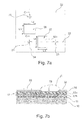
- the cantilever structures 115 and 116 are partially surrounded, in the substrate plane, by respective recesses 110b and 110a etched from the main surface 121 in the reference plane.
- the depth of the recesses with respect to the reference plane is greater than the thickness of the cantilever structures and preferably uncovers the substrate 120, by removing the layer or plurality of layers 122.
- the hinge structure is arranged recessed with respect to the reference plane 121, there is a further connecting wall (not visible in figure 1 ) that the conductive strips 109 must pass through to reach the main surface 121 of the sensor device where the external terminals, for example the pads 108, are typically positioned.
- the connecting wall between the upper surface of the hinge structures 113 and 114 and the reference surface 121 extends along a respective connecting line 117 and 118 defined on the main reference surface 121.
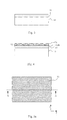
- an (elastically deformable) "strained" structure 12 is formed on the sacrificial layer 11, said structure comprising a plurality of films with different lattice constant generating a strain state in the structure, due to the elongation and/or to the compression of at least one film of the plurality of films.
- the sacrificial layer 11 and the structure 12 are made from semiconducting materials epitaxially grown on the substrate 10, in particular by means of Molecular Beam Epitaxy (MBE).
- MBE Molecular Beam Epitaxy
- the strained structure 12 comprises a succession of at least two films alternately compressed and elongated. The number of films alternately compressed and elongated comprised in the strained structure depends on the materials used and on the thickness of the films.
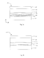
- the heterostructure of each sensor unit comprises a plurality of layers, a first layer of said plurality being a magneto-sensitive layer and a second layer being an upper contact layer (e.g., cap layer) arranged on the remaining layers of the plurality, where the heterostructure includes a mesa structure that extends vertically (i.e.
- the structure is immersed in a bath of HF:H 2 O 1:5 that dissolves the AlAs without significantly etching the bi-film In x Ga (1-x) As/GaAs or the heterostructure of GaAs and ternary alloys based upon GaAs.
- the layer of AlAs has a thickness of at least 50 nm and ranges between 50 and 100 nm so as to ensure an even penetration of the etching solution from the vertical walls along the layer, i.e. along the plane (x,y).
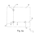
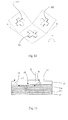
- Figure 12 schematically and partially illustrates a triaxial sensor device, in which the two out-of-plane sensor units 302 and 303 are arranged at respective angles ⁇ and ⁇ with respect to the plane (x,y) of the third sensor unit 301.
- the plane on which the sensor unit 302 is arranged is parallel to the axis x and is inclined with respect to the axis y of the angle ⁇
- the plane on which the sensor unit 303 is arranged is parallel to the axis y and is inclined with respect to the axis x of the angle ⁇ .
Landscapes
- Physics & Mathematics (AREA)
- Condensed Matter Physics & Semiconductors (AREA)
- General Physics & Mathematics (AREA)
- Hall/Mr Elements (AREA)
- Measuring Magnetic Variables (AREA)
- Measuring Fluid Pressure (AREA)
Applications Claiming Priority (1)
| Application Number | Priority Date | Filing Date | Title |
|---|---|---|---|
| IT000972A ITMI20090972A1 (it) | 2009-06-03 | 2009-06-03 | Dispositivo sensore magnetico triassiale integrato. |
Publications (2)
| Publication Number | Publication Date |
|---|---|
| EP2261684A1 true EP2261684A1 (fr) | 2010-12-15 |
| EP2261684B1 EP2261684B1 (fr) | 2012-02-08 |
Family
ID=42040529
Family Applications (1)
| Application Number | Title | Priority Date | Filing Date |
|---|---|---|---|
| EP10164576A Not-in-force EP2261684B1 (fr) | 2009-06-03 | 2010-06-01 | Capteur magnétique triaxial intégré |
Country Status (3)
| Country | Link |
|---|---|
| EP (1) | EP2261684B1 (fr) |
| AT (1) | ATE545037T1 (fr) |
| IT (1) | ITMI20090972A1 (fr) |
Cited By (7)
| Publication number | Priority date | Publication date | Assignee | Title |
|---|---|---|---|---|
| EP2381267A1 (fr) * | 2010-04-22 | 2011-10-26 | Honeywell International Inc. | Structure et procédé pour circuit flexible sur une puce |
| EP2551691A1 (fr) * | 2011-07-27 | 2013-01-30 | Paul Scherrer Institut | Procédé pour fabriquer un ensemble formant capteur Hall et ensemble formant capteur Hall |
| RU2513655C1 (ru) * | 2012-11-12 | 2014-04-20 | Федеральное государственное бюджетное учреждение науки Институт физики полупроводников им. А.В. Ржанова Сибирского отделения Российской академии наук (ИФП СО РАН) | Датчик магнитного поля и способ его изготовления |
| WO2014114401A1 (fr) * | 2013-01-24 | 2014-07-31 | Paul Scherrer Institut | Procédé de fabrication d'un ensemble de capteurs à effet hall et ensemble de capteurs à effet hall |
| AT15369U1 (de) * | 2016-02-15 | 2017-07-15 | Tridonic Gmbh & Co Kg | Multisensoranordnung |
| DE102015109110B4 (de) * | 2014-06-09 | 2019-04-04 | Infineon Technologies Ag | Vorrichtung und Sensoranordnung |
| CN111044942A (zh) * | 2018-10-11 | 2020-04-21 | Tdk株式会社 | 磁传感器装置 |
Citations (7)
| Publication number | Priority date | Publication date | Assignee | Title |
|---|---|---|---|---|
| WO1996002848A1 (fr) * | 1994-07-20 | 1996-02-01 | Honeywell Inc. | Encapsulation triaxiale |
| US5672967A (en) * | 1995-09-19 | 1997-09-30 | Southwest Research Institute | Compact tri-axial fluxgate magnetometer and housing with unitary orthogonal sensor substrate |
| US20020056202A1 (en) * | 2000-10-16 | 2002-05-16 | Yasuhiro Tamura | Three-axis magnetic sensor, an omnidirectional magnetic sensor and an azimuth measureing method using the same |
| US20070035294A1 (en) | 2004-06-03 | 2007-02-15 | Honeywell International Inc. | Integrated Three-Dimensional Magnetic Sensing Device and Method to Fabricate an Integrated Three-Dimensional Magnetic Sensing Device |
| US20080169807A1 (en) * | 2005-03-17 | 2008-07-17 | Hiroshi Naito | Magnetic Sensor and Manufacturing Method Therefor |
| US20080217288A1 (en) | 2005-01-21 | 2008-09-11 | Marcus Breuer | Method of manufacturing a magnetic sensor with tilted magnetoresistive structures |
| US20090058411A1 (en) * | 2007-08-28 | 2009-03-05 | Ngk Insulators, Ltd. | Magnetic sensor, hall element, hall ic, magnetoresistive effect element, method of fabricating hall element, and method of fabricating magnetoresistive effect element |
-
2009
- 2009-06-03 IT IT000972A patent/ITMI20090972A1/it unknown
-
2010
- 2010-06-01 AT AT10164576T patent/ATE545037T1/de active
- 2010-06-01 EP EP10164576A patent/EP2261684B1/fr not_active Not-in-force
Patent Citations (7)
| Publication number | Priority date | Publication date | Assignee | Title |
|---|---|---|---|---|
| WO1996002848A1 (fr) * | 1994-07-20 | 1996-02-01 | Honeywell Inc. | Encapsulation triaxiale |
| US5672967A (en) * | 1995-09-19 | 1997-09-30 | Southwest Research Institute | Compact tri-axial fluxgate magnetometer and housing with unitary orthogonal sensor substrate |
| US20020056202A1 (en) * | 2000-10-16 | 2002-05-16 | Yasuhiro Tamura | Three-axis magnetic sensor, an omnidirectional magnetic sensor and an azimuth measureing method using the same |
| US20070035294A1 (en) | 2004-06-03 | 2007-02-15 | Honeywell International Inc. | Integrated Three-Dimensional Magnetic Sensing Device and Method to Fabricate an Integrated Three-Dimensional Magnetic Sensing Device |
| US20080217288A1 (en) | 2005-01-21 | 2008-09-11 | Marcus Breuer | Method of manufacturing a magnetic sensor with tilted magnetoresistive structures |
| US20080169807A1 (en) * | 2005-03-17 | 2008-07-17 | Hiroshi Naito | Magnetic Sensor and Manufacturing Method Therefor |
| US20090058411A1 (en) * | 2007-08-28 | 2009-03-05 | Ngk Insulators, Ltd. | Magnetic sensor, hall element, hall ic, magnetoresistive effect element, method of fabricating hall element, and method of fabricating magnetoresistive effect element |
Non-Patent Citations (6)
| Title |
|---|
| "Nano-tesla magnetic field magnetometry using an lnGaAs-AIGaAs-GaAs 2DEG Hall sensor", SENSORS AND ACTUATORS A, vol. 102, 2003, pages 216 - 222 |
| D.R. POPOVIC ET AL.: "Three-axis Teslameter With Integrated Hall Probe", IEEE TRANSACTIONS ON INSTRUMENTATION AND MEASUREMENT, vol. 56, no. 4, 2007, pages 1396 - 1402 |
| M. MORVIC; J. BETKO: "Planar effect in Hall sensors made from InPlInGaAs heterostructures", SENSORS AND ACTUATORS A, vol. 120, 2005, pages 130 - 133 |
| P. KEJIK ET AL.: "First fully CMOS-integrated 3D Hall probe", ACTUATORS AND MICROSYSTEMS, vol. 1, 2005, pages 317 - 320 |
| S. IIDA; K. ITO: "Selective Etching of Gallium Arsenide Crystals in H2S04-H202-H20 System", JOURNAL OF ELECTROCHEMICAL SOCIETY, vol. 118-5, 1971, pages 768 |
| V. YA. PRINZ: "A new concept in fabricating building blocks for nanoelectronic and nanomechanic devices", MICROELECTRONIC ENGINEERING, vol. 69, 2003, pages 466 - 475 |
Cited By (10)
| Publication number | Priority date | Publication date | Assignee | Title |
|---|---|---|---|---|
| EP2381267A1 (fr) * | 2010-04-22 | 2011-10-26 | Honeywell International Inc. | Structure et procédé pour circuit flexible sur une puce |
| EP2551691A1 (fr) * | 2011-07-27 | 2013-01-30 | Paul Scherrer Institut | Procédé pour fabriquer un ensemble formant capteur Hall et ensemble formant capteur Hall |
| WO2013014203A1 (fr) * | 2011-07-27 | 2013-01-31 | Paul Scherrer Institut | Procédé de fabrication d'un ensemble de capteurs à effet hall et ensemble de capteurs à effet hall |
| RU2513655C1 (ru) * | 2012-11-12 | 2014-04-20 | Федеральное государственное бюджетное учреждение науки Институт физики полупроводников им. А.В. Ржанова Сибирского отделения Российской академии наук (ИФП СО РАН) | Датчик магнитного поля и способ его изготовления |
| WO2014114401A1 (fr) * | 2013-01-24 | 2014-07-31 | Paul Scherrer Institut | Procédé de fabrication d'un ensemble de capteurs à effet hall et ensemble de capteurs à effet hall |
| US9915708B2 (en) | 2013-01-24 | 2018-03-13 | Paul Scherrer Institut | Method for manufacturing a hall sensor assembly and a hall sensor assembly |
| DE102015109110B4 (de) * | 2014-06-09 | 2019-04-04 | Infineon Technologies Ag | Vorrichtung und Sensoranordnung |
| AT15369U1 (de) * | 2016-02-15 | 2017-07-15 | Tridonic Gmbh & Co Kg | Multisensoranordnung |
| CN111044942A (zh) * | 2018-10-11 | 2020-04-21 | Tdk株式会社 | 磁传感器装置 |
| CN111044942B (zh) * | 2018-10-11 | 2022-08-05 | Tdk株式会社 | 磁传感器装置 |
Also Published As
| Publication number | Publication date |
|---|---|
| ATE545037T1 (de) | 2012-02-15 |
| EP2261684B1 (fr) | 2012-02-08 |
| ITMI20090972A1 (it) | 2010-12-04 |
Similar Documents
| Publication | Publication Date | Title |
|---|---|---|
| EP2261684B1 (fr) | Capteur magnétique triaxial intégré | |
| Vorob’ev et al. | Giant asymmetry of the longitudinal magnetoresistance in high-mobility two-dimensional electron gas on a cylindrical surface | |
| EP2421043B1 (fr) | Dispositif de points quantiques | |
| WO2005106417A2 (fr) | Capteurs de souche fondes sur des fils et des reseaux de piezoresistance a nanofils | |
| KR20100056960A (ko) | 스핀-분극 전하 운반체 소자 | |
| CN110911548B (zh) | 具有工作温度实时监控功能的高温三维霍尔传感器及其制作方法 | |
| Brook et al. | Micromachined III–V cantilevers for AFM-tracking scanning Hall probe microscopy | |
| US9164153B2 (en) | Methods and apparatuses for low-noise magnetic sensors | |
| US10379175B2 (en) | Low-noise magnetic sensors | |
| Chu et al. | Piezoelectric polarization-induced two dimensional electron gases in AlGaN/GaN heteroepitaxial structures: Application for micro-pressure sensors | |
| CN102507978B (zh) | 基于e指数半导体器件的嵌入式高灵敏度微加速度计 | |
| Yang et al. | Characterization of one-dimensional quantum channels in InAs/AlSb | |
| Fujisada | Effects of diffusion current on galvanomagnetic properties in thin intrinsic InSb at room temperature | |
| Geng et al. | Integration of ZnO nanorods with MOS capacitor for self-powered force sensors and nanogenerators | |
| Lee et al. | Fabrication and characterization of one‐and zero‐dimensional electron systems | |
| EP2133931A1 (fr) | Dispositif de magnétorésistance | |
| Hsu et al. | Piezoresistive response induced by piezoelectric charges in n-type GaAs mesa resistors for application in stress transducers | |
| Borisov et al. | Semiconductor structures with a one-dimensional quantum channel and in-plane side gates fabricated by pulse force nanolithography | |
| Pomar et al. | Improving electrical contact quality and extraordinary magnetoresistance in high mobility III-V semiconductors | |
| KR101803288B1 (ko) | 나노 압력 센싱 소자 및 방법 | |
| RU2513655C1 (ru) | Датчик магнитного поля и способ его изготовления | |
| Vdovin et al. | Spin splitting of X-valley-related donor impurity states in an AlAs barrier | |
| Bui et al. | Characterization of the piezoresistive effect and temperature coefficient of resistance in single crystalline silicon nanowires | |
| RU2849835C1 (ru) | Преобразователь магнитного поля | |
| Weber et al. | Fabrication of an array of single-electron transistors for a scanning probe microscope sensor |
Legal Events
| Date | Code | Title | Description |
|---|---|---|---|
| PUAI | Public reference made under article 153(3) epc to a published international application that has entered the european phase |
Free format text: ORIGINAL CODE: 0009012 |
|
| AK | Designated contracting states |
Kind code of ref document: A1 Designated state(s): AL AT BE BG CH CY CZ DE DK EE ES FI FR GB GR HR HU IE IS IT LI LT LU LV MC MK MT NL NO PL PT RO SE SI SK SM TR |
|
| AX | Request for extension of the european patent |
Extension state: BA ME RS |
|
| RIN1 | Information on inventor provided before grant (corrected) |
Inventor name: GIORDANO, CRISTIAN Inventor name: CINGOLANI, ROBERTO Inventor name: SILEO, LEONARDO Inventor name: TODARO, MARIA TERESA Inventor name: TASCO, VITTORIANNA Inventor name: PASSASEO, ADRIANA Inventor name: DE VITTORIO, MASSIMO |
|
| 17P | Request for examination filed |
Effective date: 20110518 |
|
| RIC1 | Information provided on ipc code assigned before grant |
Ipc: G01R 33/00 20060101ALI20110628BHEP Ipc: G01R 33/02 20060101AFI20110628BHEP |
|
| GRAP | Despatch of communication of intention to grant a patent |
Free format text: ORIGINAL CODE: EPIDOSNIGR1 |
|
| GRAS | Grant fee paid |
Free format text: ORIGINAL CODE: EPIDOSNIGR3 |
|
| GRAA | (expected) grant |
Free format text: ORIGINAL CODE: 0009210 |
|
| AK | Designated contracting states |
Kind code of ref document: B1 Designated state(s): AL AT BE BG CH CY CZ DE DK EE ES FI FR GB GR HR HU IE IS IT LI LT LU LV MC MK MT NL NO PL PT RO SE SI SK SM TR |
|
| REG | Reference to a national code |
Ref country code: GB Ref legal event code: FG4D |
|
| REG | Reference to a national code |
Ref country code: AT Ref legal event code: REF Ref document number: 545037 Country of ref document: AT Kind code of ref document: T Effective date: 20120215 Ref country code: CH Ref legal event code: EP |
|
| REG | Reference to a national code |
Ref country code: DE Ref legal event code: R096 Ref document number: 602010000805 Country of ref document: DE Effective date: 20120405 |
|
| REG | Reference to a national code |
Ref country code: NL Ref legal event code: VDEP Effective date: 20120208 |
|
| LTIE | Lt: invalidation of european patent or patent extension |
Effective date: 20120208 |
|
| PG25 | Lapsed in a contracting state [announced via postgrant information from national office to epo] |
Ref country code: IS Free format text: LAPSE BECAUSE OF FAILURE TO SUBMIT A TRANSLATION OF THE DESCRIPTION OR TO PAY THE FEE WITHIN THE PRESCRIBED TIME-LIMIT Effective date: 20120608 Ref country code: LT Free format text: LAPSE BECAUSE OF FAILURE TO SUBMIT A TRANSLATION OF THE DESCRIPTION OR TO PAY THE FEE WITHIN THE PRESCRIBED TIME-LIMIT Effective date: 20120208 Ref country code: NL Free format text: LAPSE BECAUSE OF FAILURE TO SUBMIT A TRANSLATION OF THE DESCRIPTION OR TO PAY THE FEE WITHIN THE PRESCRIBED TIME-LIMIT Effective date: 20120208 Ref country code: NO Free format text: LAPSE BECAUSE OF FAILURE TO SUBMIT A TRANSLATION OF THE DESCRIPTION OR TO PAY THE FEE WITHIN THE PRESCRIBED TIME-LIMIT Effective date: 20120508 Ref country code: HR Free format text: LAPSE BECAUSE OF FAILURE TO SUBMIT A TRANSLATION OF THE DESCRIPTION OR TO PAY THE FEE WITHIN THE PRESCRIBED TIME-LIMIT Effective date: 20120208 |
|
| PG25 | Lapsed in a contracting state [announced via postgrant information from national office to epo] |
Ref country code: PL Free format text: LAPSE BECAUSE OF FAILURE TO SUBMIT A TRANSLATION OF THE DESCRIPTION OR TO PAY THE FEE WITHIN THE PRESCRIBED TIME-LIMIT Effective date: 20120208 Ref country code: PT Free format text: LAPSE BECAUSE OF FAILURE TO SUBMIT A TRANSLATION OF THE DESCRIPTION OR TO PAY THE FEE WITHIN THE PRESCRIBED TIME-LIMIT Effective date: 20120608 Ref country code: GR Free format text: LAPSE BECAUSE OF FAILURE TO SUBMIT A TRANSLATION OF THE DESCRIPTION OR TO PAY THE FEE WITHIN THE PRESCRIBED TIME-LIMIT Effective date: 20120509 Ref country code: BE Free format text: LAPSE BECAUSE OF FAILURE TO SUBMIT A TRANSLATION OF THE DESCRIPTION OR TO PAY THE FEE WITHIN THE PRESCRIBED TIME-LIMIT Effective date: 20120208 Ref country code: FI Free format text: LAPSE BECAUSE OF FAILURE TO SUBMIT A TRANSLATION OF THE DESCRIPTION OR TO PAY THE FEE WITHIN THE PRESCRIBED TIME-LIMIT Effective date: 20120208 Ref country code: LV Free format text: LAPSE BECAUSE OF FAILURE TO SUBMIT A TRANSLATION OF THE DESCRIPTION OR TO PAY THE FEE WITHIN THE PRESCRIBED TIME-LIMIT Effective date: 20120208 |
|
| REG | Reference to a national code |
Ref country code: AT Ref legal event code: MK05 Ref document number: 545037 Country of ref document: AT Kind code of ref document: T Effective date: 20120208 |
|
| PG25 | Lapsed in a contracting state [announced via postgrant information from national office to epo] |
Ref country code: CY Free format text: LAPSE BECAUSE OF FAILURE TO SUBMIT A TRANSLATION OF THE DESCRIPTION OR TO PAY THE FEE WITHIN THE PRESCRIBED TIME-LIMIT Effective date: 20120208 |
|
| PG25 | Lapsed in a contracting state [announced via postgrant information from national office to epo] |
Ref country code: SI Free format text: LAPSE BECAUSE OF FAILURE TO SUBMIT A TRANSLATION OF THE DESCRIPTION OR TO PAY THE FEE WITHIN THE PRESCRIBED TIME-LIMIT Effective date: 20120208 Ref country code: SE Free format text: LAPSE BECAUSE OF FAILURE TO SUBMIT A TRANSLATION OF THE DESCRIPTION OR TO PAY THE FEE WITHIN THE PRESCRIBED TIME-LIMIT Effective date: 20120208 Ref country code: EE Free format text: LAPSE BECAUSE OF FAILURE TO SUBMIT A TRANSLATION OF THE DESCRIPTION OR TO PAY THE FEE WITHIN THE PRESCRIBED TIME-LIMIT Effective date: 20120208 Ref country code: RO Free format text: LAPSE BECAUSE OF FAILURE TO SUBMIT A TRANSLATION OF THE DESCRIPTION OR TO PAY THE FEE WITHIN THE PRESCRIBED TIME-LIMIT Effective date: 20120208 Ref country code: DK Free format text: LAPSE BECAUSE OF FAILURE TO SUBMIT A TRANSLATION OF THE DESCRIPTION OR TO PAY THE FEE WITHIN THE PRESCRIBED TIME-LIMIT Effective date: 20120208 Ref country code: CZ Free format text: LAPSE BECAUSE OF FAILURE TO SUBMIT A TRANSLATION OF THE DESCRIPTION OR TO PAY THE FEE WITHIN THE PRESCRIBED TIME-LIMIT Effective date: 20120208 |
|
| PG25 | Lapsed in a contracting state [announced via postgrant information from national office to epo] |
Ref country code: SK Free format text: LAPSE BECAUSE OF FAILURE TO SUBMIT A TRANSLATION OF THE DESCRIPTION OR TO PAY THE FEE WITHIN THE PRESCRIBED TIME-LIMIT Effective date: 20120208 |
|
| PLBE | No opposition filed within time limit |
Free format text: ORIGINAL CODE: 0009261 |
|
| STAA | Information on the status of an ep patent application or granted ep patent |
Free format text: STATUS: NO OPPOSITION FILED WITHIN TIME LIMIT |
|
| 26N | No opposition filed |
Effective date: 20121109 |
|
| PG25 | Lapsed in a contracting state [announced via postgrant information from national office to epo] |
Ref country code: AT Free format text: LAPSE BECAUSE OF FAILURE TO SUBMIT A TRANSLATION OF THE DESCRIPTION OR TO PAY THE FEE WITHIN THE PRESCRIBED TIME-LIMIT Effective date: 20120208 Ref country code: MC Free format text: LAPSE BECAUSE OF NON-PAYMENT OF DUE FEES Effective date: 20120630 |
|
| PG25 | Lapsed in a contracting state [announced via postgrant information from national office to epo] |
Ref country code: MK Free format text: LAPSE BECAUSE OF FAILURE TO SUBMIT A TRANSLATION OF THE DESCRIPTION OR TO PAY THE FEE WITHIN THE PRESCRIBED TIME-LIMIT Effective date: 20120208 |
|
| REG | Reference to a national code |
Ref country code: DE Ref legal event code: R097 Ref document number: 602010000805 Country of ref document: DE Effective date: 20121109 |
|
| REG | Reference to a national code |
Ref country code: IE Ref legal event code: MM4A |
|
| PG25 | Lapsed in a contracting state [announced via postgrant information from national office to epo] |
Ref country code: IE Free format text: LAPSE BECAUSE OF NON-PAYMENT OF DUE FEES Effective date: 20120601 Ref country code: ES Free format text: LAPSE BECAUSE OF FAILURE TO SUBMIT A TRANSLATION OF THE DESCRIPTION OR TO PAY THE FEE WITHIN THE PRESCRIBED TIME-LIMIT Effective date: 20120519 |
|
| PG25 | Lapsed in a contracting state [announced via postgrant information from national office to epo] |
Ref country code: BG Free format text: LAPSE BECAUSE OF FAILURE TO SUBMIT A TRANSLATION OF THE DESCRIPTION OR TO PAY THE FEE WITHIN THE PRESCRIBED TIME-LIMIT Effective date: 20120508 Ref country code: MT Free format text: LAPSE BECAUSE OF FAILURE TO SUBMIT A TRANSLATION OF THE DESCRIPTION OR TO PAY THE FEE WITHIN THE PRESCRIBED TIME-LIMIT Effective date: 20120208 |
|
| PG25 | Lapsed in a contracting state [announced via postgrant information from national office to epo] |
Ref country code: AL Free format text: LAPSE BECAUSE OF FAILURE TO SUBMIT A TRANSLATION OF THE DESCRIPTION OR TO PAY THE FEE WITHIN THE PRESCRIBED TIME-LIMIT Effective date: 20120208 |
|
| PG25 | Lapsed in a contracting state [announced via postgrant information from national office to epo] |
Ref country code: TR Free format text: LAPSE BECAUSE OF FAILURE TO SUBMIT A TRANSLATION OF THE DESCRIPTION OR TO PAY THE FEE WITHIN THE PRESCRIBED TIME-LIMIT Effective date: 20120208 |
|
| PG25 | Lapsed in a contracting state [announced via postgrant information from national office to epo] |
Ref country code: SM Free format text: LAPSE BECAUSE OF FAILURE TO SUBMIT A TRANSLATION OF THE DESCRIPTION OR TO PAY THE FEE WITHIN THE PRESCRIBED TIME-LIMIT Effective date: 20120208 Ref country code: LU Free format text: LAPSE BECAUSE OF NON-PAYMENT OF DUE FEES Effective date: 20120601 |
|
| PG25 | Lapsed in a contracting state [announced via postgrant information from national office to epo] |
Ref country code: HU Free format text: LAPSE BECAUSE OF FAILURE TO SUBMIT A TRANSLATION OF THE DESCRIPTION OR TO PAY THE FEE WITHIN THE PRESCRIBED TIME-LIMIT Effective date: 20100601 |
|
| PGFP | Annual fee paid to national office [announced via postgrant information from national office to epo] |
Ref country code: GB Payment date: 20140528 Year of fee payment: 5 |
|
| PGFP | Annual fee paid to national office [announced via postgrant information from national office to epo] |
Ref country code: DE Payment date: 20140625 Year of fee payment: 5 Ref country code: IT Payment date: 20140616 Year of fee payment: 5 |
|
| PGFP | Annual fee paid to national office [announced via postgrant information from national office to epo] |
Ref country code: FR Payment date: 20140609 Year of fee payment: 5 |
|
| REG | Reference to a national code |
Ref country code: CH Ref legal event code: PL |
|
| PG25 | Lapsed in a contracting state [announced via postgrant information from national office to epo] |
Ref country code: CH Free format text: LAPSE BECAUSE OF NON-PAYMENT OF DUE FEES Effective date: 20140630 Ref country code: LI Free format text: LAPSE BECAUSE OF NON-PAYMENT OF DUE FEES Effective date: 20140630 |
|
| REG | Reference to a national code |
Ref country code: DE Ref legal event code: R119 Ref document number: 602010000805 Country of ref document: DE |
|
| PG25 | Lapsed in a contracting state [announced via postgrant information from national office to epo] |
Ref country code: IT Free format text: LAPSE BECAUSE OF NON-PAYMENT OF DUE FEES Effective date: 20150601 |
|
| GBPC | Gb: european patent ceased through non-payment of renewal fee |
Effective date: 20150601 |
|
| REG | Reference to a national code |
Ref country code: FR Ref legal event code: ST Effective date: 20160229 |
|
| PG25 | Lapsed in a contracting state [announced via postgrant information from national office to epo] |
Ref country code: DE Free format text: LAPSE BECAUSE OF NON-PAYMENT OF DUE FEES Effective date: 20160101 Ref country code: GB Free format text: LAPSE BECAUSE OF NON-PAYMENT OF DUE FEES Effective date: 20150601 |
|
| PG25 | Lapsed in a contracting state [announced via postgrant information from national office to epo] |
Ref country code: FR Free format text: LAPSE BECAUSE OF NON-PAYMENT OF DUE FEES Effective date: 20150630 |