EP2261991A2 - Méthode de fabrication d'un transistor à effet de champ et à haute tension - Google Patents
Méthode de fabrication d'un transistor à effet de champ et à haute tension Download PDFInfo
- Publication number
- EP2261991A2 EP2261991A2 EP20100182534 EP10182534A EP2261991A2 EP 2261991 A2 EP2261991 A2 EP 2261991A2 EP 20100182534 EP20100182534 EP 20100182534 EP 10182534 A EP10182534 A EP 10182534A EP 2261991 A2 EP2261991 A2 EP 2261991A2
- Authority
- EP
- European Patent Office
- Prior art keywords
- region
- buried
- substrate
- well region
- drain
- Prior art date
- Legal status (The legal status is an assumption and is not a legal conclusion. Google has not performed a legal analysis and makes no representation as to the accuracy of the status listed.)
- Granted
Links
Images





Classifications
-
- H—ELECTRICITY
- H10—SEMICONDUCTOR DEVICES; ELECTRIC SOLID-STATE DEVICES NOT OTHERWISE PROVIDED FOR
- H10D—INORGANIC ELECTRIC SEMICONDUCTOR DEVICES
- H10D62/00—Semiconductor bodies, or regions thereof, of devices having potential barriers
- H10D62/10—Shapes, relative sizes or dispositions of the regions of the semiconductor bodies; Shapes of the semiconductor bodies
- H10D62/13—Semiconductor regions connected to electrodes carrying current to be rectified, amplified or switched, e.g. source or drain regions
- H10D62/149—Source or drain regions of field-effect devices
- H10D62/151—Source or drain regions of field-effect devices of IGFETs
-
- H—ELECTRICITY
- H10—SEMICONDUCTOR DEVICES; ELECTRIC SOLID-STATE DEVICES NOT OTHERWISE PROVIDED FOR
- H10D—INORGANIC ELECTRIC SEMICONDUCTOR DEVICES
- H10D30/00—Field-effect transistors [FET]
- H10D30/01—Manufacture or treatment
- H10D30/021—Manufacture or treatment of FETs having insulated gates [IGFET]
- H10D30/0221—Manufacture or treatment of FETs having insulated gates [IGFET] having asymmetry in the channel direction, e.g. lateral high-voltage MISFETs having drain offset region or extended-drain MOSFETs [EDMOS]
-
- H—ELECTRICITY
- H10—SEMICONDUCTOR DEVICES; ELECTRIC SOLID-STATE DEVICES NOT OTHERWISE PROVIDED FOR
- H10D—INORGANIC ELECTRIC SEMICONDUCTOR DEVICES
- H10D30/00—Field-effect transistors [FET]
- H10D30/01—Manufacture or treatment
- H10D30/021—Manufacture or treatment of FETs having insulated gates [IGFET]
- H10D30/028—Manufacture or treatment of FETs having insulated gates [IGFET] of double-diffused metal oxide semiconductor [DMOS] FETs
- H10D30/0281—Manufacture or treatment of FETs having insulated gates [IGFET] of double-diffused metal oxide semiconductor [DMOS] FETs of lateral DMOS [LDMOS] FETs
-
- H—ELECTRICITY
- H10—SEMICONDUCTOR DEVICES; ELECTRIC SOLID-STATE DEVICES NOT OTHERWISE PROVIDED FOR
- H10D—INORGANIC ELECTRIC SEMICONDUCTOR DEVICES
- H10D30/00—Field-effect transistors [FET]
- H10D30/60—Insulated-gate field-effect transistors [IGFET]
- H10D30/601—Insulated-gate field-effect transistors [IGFET] having lightly-doped drain or source extensions, e.g. LDD IGFETs or DDD IGFETs
- H10D30/603—Insulated-gate field-effect transistors [IGFET] having lightly-doped drain or source extensions, e.g. LDD IGFETs or DDD IGFETs having asymmetry in the channel direction, e.g. lateral high-voltage MISFETs having drain offset region or extended drain IGFETs [EDMOS]
-
- H—ELECTRICITY
- H10—SEMICONDUCTOR DEVICES; ELECTRIC SOLID-STATE DEVICES NOT OTHERWISE PROVIDED FOR
- H10D—INORGANIC ELECTRIC SEMICONDUCTOR DEVICES
- H10D30/00—Field-effect transistors [FET]
- H10D30/60—Insulated-gate field-effect transistors [IGFET]
- H10D30/64—Double-diffused metal-oxide semiconductor [DMOS] FETs
- H10D30/65—Lateral DMOS [LDMOS] FETs
-
- H—ELECTRICITY
- H10—SEMICONDUCTOR DEVICES; ELECTRIC SOLID-STATE DEVICES NOT OTHERWISE PROVIDED FOR
- H10D—INORGANIC ELECTRIC SEMICONDUCTOR DEVICES
- H10D62/00—Semiconductor bodies, or regions thereof, of devices having potential barriers
- H10D62/10—Shapes, relative sizes or dispositions of the regions of the semiconductor bodies; Shapes of the semiconductor bodies
- H10D62/102—Constructional design considerations for preventing surface leakage or controlling electric field concentration
- H10D62/103—Constructional design considerations for preventing surface leakage or controlling electric field concentration for increasing or controlling the breakdown voltage of reverse-biased devices
- H10D62/105—Constructional design considerations for preventing surface leakage or controlling electric field concentration for increasing or controlling the breakdown voltage of reverse-biased devices by having particular doping profiles, shapes or arrangements of PN junctions; by having supplementary regions, e.g. junction termination extension [JTE]
- H10D62/109—Reduced surface field [RESURF] PN junction structures
- H10D62/111—Multiple RESURF structures, e.g. double RESURF or 3D-RESURF structures
-
- H—ELECTRICITY
- H10—SEMICONDUCTOR DEVICES; ELECTRIC SOLID-STATE DEVICES NOT OTHERWISE PROVIDED FOR
- H10D—INORGANIC ELECTRIC SEMICONDUCTOR DEVICES
- H10D62/00—Semiconductor bodies, or regions thereof, of devices having potential barriers
- H10D62/10—Shapes, relative sizes or dispositions of the regions of the semiconductor bodies; Shapes of the semiconductor bodies
- H10D62/13—Semiconductor regions connected to electrodes carrying current to be rectified, amplified or switched, e.g. source or drain regions
- H10D62/149—Source or drain regions of field-effect devices
- H10D62/151—Source or drain regions of field-effect devices of IGFETs
- H10D62/152—Source regions of DMOS transistors
-
- H—ELECTRICITY
- H10—SEMICONDUCTOR DEVICES; ELECTRIC SOLID-STATE DEVICES NOT OTHERWISE PROVIDED FOR
- H10D—INORGANIC ELECTRIC SEMICONDUCTOR DEVICES
- H10D62/00—Semiconductor bodies, or regions thereof, of devices having potential barriers
- H10D62/10—Shapes, relative sizes or dispositions of the regions of the semiconductor bodies; Shapes of the semiconductor bodies
- H10D62/13—Semiconductor regions connected to electrodes carrying current to be rectified, amplified or switched, e.g. source or drain regions
- H10D62/149—Source or drain regions of field-effect devices
- H10D62/151—Source or drain regions of field-effect devices of IGFETs
- H10D62/156—Drain regions of DMOS transistors
-
- H—ELECTRICITY
- H10—SEMICONDUCTOR DEVICES; ELECTRIC SOLID-STATE DEVICES NOT OTHERWISE PROVIDED FOR
- H10P—GENERIC PROCESSES OR APPARATUS FOR THE MANUFACTURE OR TREATMENT OF DEVICES COVERED BY CLASS H10
- H10P30/00—Ion implantation into wafers, substrates or parts of devices
- H10P30/20—Ion implantation into wafers, substrates or parts of devices into semiconductor materials, e.g. for doping
- H10P30/22—Ion implantation into wafers, substrates or parts of devices into semiconductor materials, e.g. for doping using masks
-
- H—ELECTRICITY
- H10—SEMICONDUCTOR DEVICES; ELECTRIC SOLID-STATE DEVICES NOT OTHERWISE PROVIDED FOR
- H10D—INORGANIC ELECTRIC SEMICONDUCTOR DEVICES
- H10D62/00—Semiconductor bodies, or regions thereof, of devices having potential barriers
- H10D62/10—Shapes, relative sizes or dispositions of the regions of the semiconductor bodies; Shapes of the semiconductor bodies
- H10D62/124—Shapes, relative sizes or dispositions of the regions of semiconductor bodies or of junctions between the regions
- H10D62/126—Top-view geometrical layouts of the regions or the junctions
-
- H—ELECTRICITY
- H10—SEMICONDUCTOR DEVICES; ELECTRIC SOLID-STATE DEVICES NOT OTHERWISE PROVIDED FOR
- H10D—INORGANIC ELECTRIC SEMICONDUCTOR DEVICES
- H10D62/00—Semiconductor bodies, or regions thereof, of devices having potential barriers
- H10D62/10—Shapes, relative sizes or dispositions of the regions of the semiconductor bodies; Shapes of the semiconductor bodies
- H10D62/17—Semiconductor regions connected to electrodes not carrying current to be rectified, amplified or switched, e.g. channel regions
- H10D62/213—Channel regions of field-effect devices
- H10D62/221—Channel regions of field-effect devices of FETs
- H10D62/235—Channel regions of field-effect devices of FETs of IGFETs
- H10D62/299—Channel regions of field-effect devices of FETs of IGFETs having lateral doping variations
- H10D62/307—Channel regions of field-effect devices of FETs of IGFETs having lateral doping variations the doping variations being parallel to the channel lengths
-
- H—ELECTRICITY
- H10—SEMICONDUCTOR DEVICES; ELECTRIC SOLID-STATE DEVICES NOT OTHERWISE PROVIDED FOR
- H10D—INORGANIC ELECTRIC SEMICONDUCTOR DEVICES
- H10D62/00—Semiconductor bodies, or regions thereof, of devices having potential barriers
- H10D62/10—Shapes, relative sizes or dispositions of the regions of the semiconductor bodies; Shapes of the semiconductor bodies
- H10D62/17—Semiconductor regions connected to electrodes not carrying current to be rectified, amplified or switched, e.g. channel regions
- H10D62/351—Substrate regions of field-effect devices
- H10D62/357—Substrate regions of field-effect devices of FETs
- H10D62/364—Substrate regions of field-effect devices of FETs of IGFETs
- H10D62/371—Inactive supplementary semiconductor regions, e.g. for preventing punch-through, improving capacity effect or leakage current
-
- H—ELECTRICITY
- H10—SEMICONDUCTOR DEVICES; ELECTRIC SOLID-STATE DEVICES NOT OTHERWISE PROVIDED FOR
- H10D—INORGANIC ELECTRIC SEMICONDUCTOR DEVICES
- H10D62/00—Semiconductor bodies, or regions thereof, of devices having potential barriers
- H10D62/10—Shapes, relative sizes or dispositions of the regions of the semiconductor bodies; Shapes of the semiconductor bodies
- H10D62/17—Semiconductor regions connected to electrodes not carrying current to be rectified, amplified or switched, e.g. channel regions
- H10D62/393—Body regions of DMOS transistors or IGBTs
-
- H—ELECTRICITY
- H10—SEMICONDUCTOR DEVICES; ELECTRIC SOLID-STATE DEVICES NOT OTHERWISE PROVIDED FOR
- H10D—INORGANIC ELECTRIC SEMICONDUCTOR DEVICES
- H10D64/00—Electrodes of devices having potential barriers
- H10D64/111—Field plates
-
- H—ELECTRICITY
- H10—SEMICONDUCTOR DEVICES; ELECTRIC SOLID-STATE DEVICES NOT OTHERWISE PROVIDED FOR
- H10D—INORGANIC ELECTRIC SEMICONDUCTOR DEVICES
- H10D64/00—Electrodes of devices having potential barriers
- H10D64/20—Electrodes characterised by their shapes, relative sizes or dispositions
- H10D64/23—Electrodes carrying the current to be rectified, amplified, oscillated or switched, e.g. sources, drains, anodes or cathodes
- H10D64/251—Source or drain electrodes for field-effect devices
- H10D64/257—Source or drain electrodes for field-effect devices for lateral devices wherein the source or drain electrodes are characterised by top-view geometrical layouts, e.g. interdigitated, semi-circular, annular or L-shaped electrodes
-
- H—ELECTRICITY
- H10—SEMICONDUCTOR DEVICES; ELECTRIC SOLID-STATE DEVICES NOT OTHERWISE PROVIDED FOR
- H10D—INORGANIC ELECTRIC SEMICONDUCTOR DEVICES
- H10D64/00—Electrodes of devices having potential barriers
- H10D64/20—Electrodes characterised by their shapes, relative sizes or dispositions
- H10D64/27—Electrodes not carrying the current to be rectified, amplified, oscillated or switched, e.g. gates
- H10D64/311—Gate electrodes for field-effect devices
- H10D64/411—Gate electrodes for field-effect devices for FETs
- H10D64/511—Gate electrodes for field-effect devices for FETs for IGFETs
- H10D64/514—Gate electrodes for field-effect devices for FETs for IGFETs characterised by the insulating layers
- H10D64/516—Gate electrodes for field-effect devices for FETs for IGFETs characterised by the insulating layers the thicknesses being non-uniform
-
- H—ELECTRICITY
- H10—SEMICONDUCTOR DEVICES; ELECTRIC SOLID-STATE DEVICES NOT OTHERWISE PROVIDED FOR
- H10D—INORGANIC ELECTRIC SEMICONDUCTOR DEVICES
- H10D64/00—Electrodes of devices having potential barriers
- H10D64/20—Electrodes characterised by their shapes, relative sizes or dispositions
- H10D64/27—Electrodes not carrying the current to be rectified, amplified, oscillated or switched, e.g. gates
- H10D64/311—Gate electrodes for field-effect devices
- H10D64/411—Gate electrodes for field-effect devices for FETs
- H10D64/511—Gate electrodes for field-effect devices for FETs for IGFETs
- H10D64/517—Gate electrodes for field-effect devices for FETs for IGFETs characterised by the conducting layers
- H10D64/519—Gate electrodes for field-effect devices for FETs for IGFETs characterised by the conducting layers characterised by their top-view geometrical layouts
Definitions
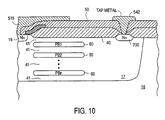
- p-type region 60 denoted PB1 is formed coincident with, and just below, the upper surface of the N-well region 17.
- the number of JFET channels is equal to the number of P-buried regions 60.
- the charge in the uppermost P-buried layer PB1 is constrained to about 1x10 12 /cm 2
- the charge in each of the remaining P-buried regions and the charge in each of the JFET channels 41 is constrained to about 2x10 12 /cm 2 .
- a spherical p-type buried layer can deplete n-type charges around it in a three-dimensional fashion.
- a spherically or other shaped buried layer can be formed to take advantage of multi-dimensional depletions.
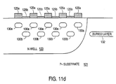
- oxide layer 125 is an optional step of the process of the present invention.
- Several benefits of not forming oxide layer 125 include reduced processing costs and a reduction in the energy required to implant the underlying buried layers. For example, without oxide layer 125 an implant energy level of about 800keV may be suitable to form a single buried layer 130.
- Figure 11 f illustrates a device structure similar to that of Figure 11e , except that in Figure 11 e the uppermost buried layer 150 (PB1) is formed just under the surface of the N-well region 123. This is accomplished by appropriate reduction of the implant energies used to form each of the buried layers 150.
- the number of JFET conduction channels 160 is identical to the number of buried layers 150.
- the maximum charge in the uppermost P-buried layer 150 (PB1) is approximately 1x10 12 /cm 2
- the maximum charge in each of the remaining P-buried layers 150 (and the charge in each of the JFET conduction channels 160) is approximately 2x10 12 /cm 2 .
- N+ source diffusion region 128 and N+ drain diffusion region 131 are appropriately masked and a dopant such as arsenic or phosphorous is implanted to form N+ source diffusion region 128 and N+ drain diffusion region 131, as shown in Figure 11 h.
- a dopant such as arsenic or phosphorous is implanted to form N+ source diffusion region 128 and N+ drain diffusion region 131, as shown in Figure 11 h.
- an optional P+ region 135 may be created adjacent to the source diffusion region 128 by ion implantation. Practitioners in the semiconductor fabrication arts will understand that it may be desirable to also form a P+ region adjacent to drain diffusion region 131.
- Figure 12 is a plot of a typical impurity concentration profile within the laterally extended drain portion of the HVFET following the process steps illustrated in Figure 11c .
- Figure 12 is for illustrative purposes only, and is not intended to limit the invention to the quantities described therein.
- the vertical axis of the graph represents the ion concentration represented as the logarithm of the number of ions per cubic centimeter.
- the horizontal axis of the graph represents the vertical distance (depth) into the semiconductor substrate 121. The depth is measured in microns from the semiconductor substrate surface.
Landscapes
- Insulated Gate Type Field-Effect Transistor (AREA)
- Junction Field-Effect Transistors (AREA)
Applications Claiming Priority (2)
| Application Number | Priority Date | Filing Date | Title |
|---|---|---|---|
| US09/245,029 US6168983B1 (en) | 1996-11-05 | 1999-02-05 | Method of making a high-voltage transistor with multiple lateral conduction layers |
| EP00908424A EP1163697A4 (fr) | 1999-02-05 | 2000-01-31 | Procede de fabrication d'un transistor haute tension avec couches laterales multiples de conduction |
Related Parent Applications (2)
| Application Number | Title | Priority Date | Filing Date |
|---|---|---|---|
| EP00908424A Division EP1163697A4 (fr) | 1999-02-05 | 2000-01-31 | Procede de fabrication d'un transistor haute tension avec couches laterales multiples de conduction |
| EP00908424.5 Division | 2000-01-31 |
Publications (3)
| Publication Number | Publication Date |
|---|---|
| EP2261991A2 true EP2261991A2 (fr) | 2010-12-15 |
| EP2261991A3 EP2261991A3 (fr) | 2011-01-05 |
| EP2261991B1 EP2261991B1 (fr) | 2017-08-23 |
Family
ID=22925032
Family Applications (3)
| Application Number | Title | Priority Date | Filing Date |
|---|---|---|---|
| EP10182534.7A Expired - Lifetime EP2261991B1 (fr) | 1999-02-05 | 2000-01-31 | Méthode de fabrication d'un transistor à effet de champ et à haute tension |
| EP00908424A Ceased EP1163697A4 (fr) | 1999-02-05 | 2000-01-31 | Procede de fabrication d'un transistor haute tension avec couches laterales multiples de conduction |
| EP10182706.1A Expired - Lifetime EP2264772B1 (fr) | 1999-02-05 | 2000-01-31 | Méthode de fabrication d'un transistor à effet de champ et à haute tension |
Family Applications After (2)
| Application Number | Title | Priority Date | Filing Date |
|---|---|---|---|
| EP00908424A Ceased EP1163697A4 (fr) | 1999-02-05 | 2000-01-31 | Procede de fabrication d'un transistor haute tension avec couches laterales multiples de conduction |
| EP10182706.1A Expired - Lifetime EP2264772B1 (fr) | 1999-02-05 | 2000-01-31 | Méthode de fabrication d'un transistor à effet de champ et à haute tension |
Country Status (4)
| Country | Link |
|---|---|
| US (1) | US6168983B1 (fr) |
| EP (3) | EP2261991B1 (fr) |
| AU (1) | AU2977000A (fr) |
| WO (1) | WO2000046851A1 (fr) |
Families Citing this family (130)
| Publication number | Priority date | Publication date | Assignee | Title |
|---|---|---|---|---|
| US6700157B2 (en) * | 1996-01-22 | 2004-03-02 | Fuji Electric Co., Ltd. | Semiconductor device |
| US6639277B2 (en) * | 1996-11-05 | 2003-10-28 | Power Integrations, Inc. | High-voltage transistor with multi-layer conduction region |
| US6207994B1 (en) * | 1996-11-05 | 2001-03-27 | Power Integrations, Inc. | High-voltage transistor with multi-layer conduction region |
| JP3988262B2 (ja) * | 1998-07-24 | 2007-10-10 | 富士電機デバイステクノロジー株式会社 | 縦型超接合半導体素子およびその製造方法 |
| DE19947020B4 (de) * | 1999-09-30 | 2006-02-23 | Infineon Technologies Ag | Kompensationsbauelement mit variabler Ladungsbilanz und dessen Herstellungsverfahren |
| US6461918B1 (en) * | 1999-12-20 | 2002-10-08 | Fairchild Semiconductor Corporation | Power MOS device with improved gate charge performance |
| GB0012137D0 (en) * | 2000-05-20 | 2000-07-12 | Koninkl Philips Electronics Nv | A semiconductor device |
| US7745289B2 (en) | 2000-08-16 | 2010-06-29 | Fairchild Semiconductor Corporation | Method of forming a FET having ultra-low on-resistance and low gate charge |
| US6696726B1 (en) * | 2000-08-16 | 2004-02-24 | Fairchild Semiconductor Corporation | Vertical MOSFET with ultra-low resistance and low gate charge |
| US6509220B2 (en) * | 2000-11-27 | 2003-01-21 | Power Integrations, Inc. | Method of fabricating a high-voltage transistor |
| US6468847B1 (en) * | 2000-11-27 | 2002-10-22 | Power Integrations, Inc. | Method of fabricating a high-voltage transistor |
| US6424007B1 (en) | 2001-01-24 | 2002-07-23 | Power Integrations, Inc. | High-voltage transistor with buried conduction layer |
| US6713813B2 (en) | 2001-01-30 | 2004-03-30 | Fairchild Semiconductor Corporation | Field effect transistor having a lateral depletion structure |
| US6818513B2 (en) * | 2001-01-30 | 2004-11-16 | Fairchild Semiconductor Corporation | Method of forming a field effect transistor having a lateral depletion structure |
| US6916745B2 (en) * | 2003-05-20 | 2005-07-12 | Fairchild Semiconductor Corporation | Structure and method for forming a trench MOSFET having self-aligned features |
| US6710403B2 (en) * | 2002-07-30 | 2004-03-23 | Fairchild Semiconductor Corporation | Dual trench power MOSFET |
| US7132712B2 (en) * | 2002-11-05 | 2006-11-07 | Fairchild Semiconductor Corporation | Trench structure having one or more diodes embedded therein adjacent a PN junction |
| US7345342B2 (en) * | 2001-01-30 | 2008-03-18 | Fairchild Semiconductor Corporation | Power semiconductor devices and methods of manufacture |
| US6803626B2 (en) | 2002-07-18 | 2004-10-12 | Fairchild Semiconductor Corporation | Vertical charge control semiconductor device |
| US6677641B2 (en) | 2001-10-17 | 2004-01-13 | Fairchild Semiconductor Corporation | Semiconductor structure with improved smaller forward voltage loss and higher blocking capability |
| FI120310B (fi) * | 2001-02-13 | 2009-09-15 | Valtion Teknillinen | Parannettu menetelmä erittyvien proteiinien tuottamiseksi sienissä |
| US6773997B2 (en) * | 2001-07-31 | 2004-08-10 | Semiconductor Components Industries, L.L.C. | Method for manufacturing a high voltage MOSFET semiconductor device with enhanced charge controllability |
| US7786533B2 (en) * | 2001-09-07 | 2010-08-31 | Power Integrations, Inc. | High-voltage vertical transistor with edge termination structure |
| US6573558B2 (en) * | 2001-09-07 | 2003-06-03 | Power Integrations, Inc. | High-voltage vertical transistor with a multi-layered extended drain structure |
| US6635544B2 (en) * | 2001-09-07 | 2003-10-21 | Power Intergrations, Inc. | Method of fabricating a high-voltage transistor with a multi-layered extended drain structure |
| US7061066B2 (en) | 2001-10-17 | 2006-06-13 | Fairchild Semiconductor Corporation | Schottky diode using charge balance structure |
| JP3546037B2 (ja) * | 2001-12-03 | 2004-07-21 | 松下電器産業株式会社 | 半導体装置の製造方法 |
| US7078296B2 (en) | 2002-01-16 | 2006-07-18 | Fairchild Semiconductor Corporation | Self-aligned trench MOSFETs and methods for making the same |
| KR100422393B1 (ko) * | 2002-01-17 | 2004-03-11 | 한국전자통신연구원 | 격자형 표류 영역 구조를 갖는 이디모스 소자 및 그 제조방법 |
| KR100859701B1 (ko) * | 2002-02-23 | 2008-09-23 | 페어차일드코리아반도체 주식회사 | 고전압 수평형 디모스 트랜지스터 및 그 제조 방법 |
| US6613622B1 (en) * | 2002-07-15 | 2003-09-02 | Semiconductor Components Industries Llc | Method of forming a semiconductor device and structure therefor |
| US7576388B1 (en) * | 2002-10-03 | 2009-08-18 | Fairchild Semiconductor Corporation | Trench-gate LDMOS structures |
| US7033891B2 (en) * | 2002-10-03 | 2006-04-25 | Fairchild Semiconductor Corporation | Trench gate laterally diffused MOSFET devices and methods for making such devices |
| US6710418B1 (en) | 2002-10-11 | 2004-03-23 | Fairchild Semiconductor Corporation | Schottky rectifier with insulation-filled trenches and method of forming the same |
| KR100948139B1 (ko) * | 2003-04-09 | 2010-03-18 | 페어차일드코리아반도체 주식회사 | 높은 브레이크다운 전압 및 낮은 온 저항을 위한 다중전류 이동 경로를 갖는 수평형 이중-확산 모스 트랜지스터 |
| JP4477309B2 (ja) * | 2003-05-09 | 2010-06-09 | Necエレクトロニクス株式会社 | 高耐圧半導体装置及びその製造方法 |
| US7638841B2 (en) | 2003-05-20 | 2009-12-29 | Fairchild Semiconductor Corporation | Power semiconductor devices and methods of manufacture |
| JP4198006B2 (ja) * | 2003-07-25 | 2008-12-17 | 株式会社リコー | 半導体装置の製造方法 |
| US7049669B2 (en) * | 2003-09-15 | 2006-05-23 | Infineon Technologies Ag | LDMOS transistor |
| US6989567B2 (en) * | 2003-10-03 | 2006-01-24 | Infineon Technologies North America Corp. | LDMOS transistor |
| KR100994719B1 (ko) * | 2003-11-28 | 2010-11-16 | 페어차일드코리아반도체 주식회사 | 슈퍼정션 반도체장치 |
| US7368777B2 (en) * | 2003-12-30 | 2008-05-06 | Fairchild Semiconductor Corporation | Accumulation device with charge balance structure and method of forming the same |
| US7119399B2 (en) * | 2004-02-27 | 2006-10-10 | Infineon Technologies Ag | LDMOS transistor |
| US7221034B2 (en) * | 2004-02-27 | 2007-05-22 | Infineon Technologies Ag | Semiconductor structure including vias |
| US20050199918A1 (en) * | 2004-03-15 | 2005-09-15 | Daniel Calafut | Optimized trench power MOSFET with integrated schottky diode |
| US7352036B2 (en) * | 2004-08-03 | 2008-04-01 | Fairchild Semiconductor Corporation | Semiconductor power device having a top-side drain using a sinker trench |
| US7265415B2 (en) * | 2004-10-08 | 2007-09-04 | Fairchild Semiconductor Corporation | MOS-gated transistor with reduced miller capacitance |
| US7365402B2 (en) * | 2005-01-06 | 2008-04-29 | Infineon Technologies Ag | LDMOS transistor |
| US20080261358A1 (en) * | 2005-02-07 | 2008-10-23 | Nxp B.V. | Manufacture of Lateral Semiconductor Devices |
| AT504998A2 (de) | 2005-04-06 | 2008-09-15 | Fairchild Semiconductor | Trenched-gate-feldeffekttransistoren und verfahren zum bilden derselben |
| US7211477B2 (en) * | 2005-05-06 | 2007-05-01 | Freescale Semiconductor, Inc. | High voltage field effect device and method |
| US7208364B2 (en) * | 2005-06-16 | 2007-04-24 | Texas Instruments Incorporated | Methods of fabricating high voltage devices |
| US8692324B2 (en) * | 2005-07-13 | 2014-04-08 | Ciclon Semiconductor Device Corp. | Semiconductor devices having charge balanced structure |
| US7385248B2 (en) * | 2005-08-09 | 2008-06-10 | Fairchild Semiconductor Corporation | Shielded gate field effect transistor with improved inter-poly dielectric |
| KR100628250B1 (ko) * | 2005-09-28 | 2006-09-27 | 동부일렉트로닉스 주식회사 | 전력용 반도체 소자 및 그의 제조방법 |
| US7446374B2 (en) | 2006-03-24 | 2008-11-04 | Fairchild Semiconductor Corporation | High density trench FET with integrated Schottky diode and method of manufacture |
| US7319256B1 (en) | 2006-06-19 | 2008-01-15 | Fairchild Semiconductor Corporation | Shielded gate trench FET with the shield and gate electrodes being connected together |
| JP2008004649A (ja) * | 2006-06-21 | 2008-01-10 | Matsushita Electric Ind Co Ltd | 半導体装置及びその製造方法 |
| JP5148852B2 (ja) * | 2006-09-07 | 2013-02-20 | 新日本無線株式会社 | 半導体装置 |
| US8093621B2 (en) | 2008-12-23 | 2012-01-10 | Power Integrations, Inc. | VTS insulated gate bipolar transistor |
| US7557406B2 (en) * | 2007-02-16 | 2009-07-07 | Power Integrations, Inc. | Segmented pillar layout for a high-voltage vertical transistor |
| US8653583B2 (en) * | 2007-02-16 | 2014-02-18 | Power Integrations, Inc. | Sensing FET integrated with a high-voltage transistor |
| US7859037B2 (en) | 2007-02-16 | 2010-12-28 | Power Integrations, Inc. | Checkerboarded high-voltage vertical transistor layout |
| DE102007034800A1 (de) * | 2007-03-26 | 2008-10-02 | X-Fab Dresden Gmbh & Co. Kg | Maskensparende Herstellung komplementärer lateraler Hochvolttransistoren mit RESURF-Struktur |
| US7626233B2 (en) * | 2007-04-23 | 2009-12-01 | Infineon Technologies Ag | LDMOS device |
| CN101868856B (zh) * | 2007-09-21 | 2014-03-12 | 飞兆半导体公司 | 用于功率器件的超结结构及制造方法 |
| US7875962B2 (en) * | 2007-10-15 | 2011-01-25 | Power Integrations, Inc. | Package for a power semiconductor device |
| US7772668B2 (en) | 2007-12-26 | 2010-08-10 | Fairchild Semiconductor Corporation | Shielded gate trench FET with multiple channels |
| US7928508B2 (en) * | 2008-04-15 | 2011-04-19 | Taiwan Semiconductor Manufacturing Company, Ltd. | Disconnected DPW structures for improving on-state performance of MOS devices |
| JP2010016180A (ja) * | 2008-07-03 | 2010-01-21 | Panasonic Corp | 半導体装置 |
| US7851857B2 (en) * | 2008-07-30 | 2010-12-14 | Freescale Semiconductor, Inc. | Dual current path LDMOSFET with graded PBL for ultra high voltage smart power applications |
| JP5296450B2 (ja) * | 2008-08-13 | 2013-09-25 | セイコーインスツル株式会社 | 半導体装置 |
| US7964912B2 (en) | 2008-09-18 | 2011-06-21 | Power Integrations, Inc. | High-voltage vertical transistor with a varied width silicon pillar |
| US20120273916A1 (en) | 2011-04-27 | 2012-11-01 | Yedinak Joseph A | Superjunction Structures for Power Devices and Methods of Manufacture |
| US8174067B2 (en) | 2008-12-08 | 2012-05-08 | Fairchild Semiconductor Corporation | Trench-based power semiconductor devices with increased breakdown voltage characteristics |
| US7871882B2 (en) | 2008-12-20 | 2011-01-18 | Power Integrations, Inc. | Method of fabricating a deep trench insulated gate bipolar transistor |
| US20100155831A1 (en) * | 2008-12-20 | 2010-06-24 | Power Integrations, Inc. | Deep trench insulated gate bipolar transistor |
| US8115457B2 (en) | 2009-07-31 | 2012-02-14 | Power Integrations, Inc. | Method and apparatus for implementing a power converter input terminal voltage discharge circuit |
| US8207455B2 (en) * | 2009-07-31 | 2012-06-26 | Power Integrations, Inc. | Power semiconductor package with bottom surface protrusions |
| US7935601B1 (en) * | 2009-09-04 | 2011-05-03 | The United States Of America As Represented By The Administrator Of National Aeronautics And Space Administration | Method for providing semiconductors having self-aligned ion implant |
| US8207577B2 (en) * | 2009-09-29 | 2012-06-26 | Power Integrations, Inc. | High-voltage transistor structure with reduced gate capacitance |
| US7893754B1 (en) | 2009-10-02 | 2011-02-22 | Power Integrations, Inc. | Temperature independent reference circuit |
| US8634218B2 (en) * | 2009-10-06 | 2014-01-21 | Power Integrations, Inc. | Monolithic AC/DC converter for generating DC supply voltage |
| CN101719515B (zh) * | 2009-11-03 | 2011-11-23 | 苏州远创达科技有限公司 | 栅下具有横向扩散埋层的ldmos器件 |
| DE102009051745B4 (de) | 2009-11-03 | 2017-09-21 | Austriamicrosystems Ag | Hochvolt-Transistor mit Mehrfach-Dielektrikum und Herstellungsverfahren |
| US8310845B2 (en) * | 2010-02-10 | 2012-11-13 | Power Integrations, Inc. | Power supply circuit with a control terminal for different functional modes of operation |
| US20110241112A1 (en) * | 2010-03-31 | 2011-10-06 | Zuniga Marco A | LDMOS Device with P-Body for Reduced Capacitance |
| US8164125B2 (en) * | 2010-05-07 | 2012-04-24 | Power Integrations, Inc. | Integrated transistor and anti-fuse as programming element for a high-voltage integrated circuit |
| TWI423423B (zh) * | 2010-06-01 | 2014-01-11 | Macronix Int Co Ltd | 半導體裝置及其製造方法 |
| US8432000B2 (en) | 2010-06-18 | 2013-04-30 | Fairchild Semiconductor Corporation | Trench MOS barrier schottky rectifier with a planar surface using CMP techniques |
| US8354716B2 (en) * | 2010-07-02 | 2013-01-15 | Macronix International Co., Ltd. | Semiconductor devices and methods of manufacturing the same |
| US8673700B2 (en) | 2011-04-27 | 2014-03-18 | Fairchild Semiconductor Corporation | Superjunction structures for power devices and methods of manufacture |
| US8836028B2 (en) | 2011-04-27 | 2014-09-16 | Fairchild Semiconductor Corporation | Superjunction structures for power devices and methods of manufacture |
| US8786010B2 (en) | 2011-04-27 | 2014-07-22 | Fairchild Semiconductor Corporation | Superjunction structures for power devices and methods of manufacture |
| US8772868B2 (en) | 2011-04-27 | 2014-07-08 | Fairchild Semiconductor Corporation | Superjunction structures for power devices and methods of manufacture |
| CN103094341A (zh) * | 2011-11-08 | 2013-05-08 | 上海华虹Nec电子有限公司 | 低导通电阻的超高压nldmos器件及其制备方法 |
| US8653600B2 (en) | 2012-06-01 | 2014-02-18 | Power Integrations, Inc. | High-voltage monolithic schottky device structure |
| KR102068842B1 (ko) * | 2013-04-16 | 2020-02-12 | 매그나칩 반도체 유한회사 | 반도체 전력소자 |
| KR101779237B1 (ko) | 2013-06-04 | 2017-09-19 | 매그나칩 반도체 유한회사 | 반도체 전력소자 및 이를 제조하는 방법 |
| US9660053B2 (en) * | 2013-07-12 | 2017-05-23 | Power Integrations, Inc. | High-voltage field-effect transistor having multiple implanted layers |
| US9455621B2 (en) | 2013-08-28 | 2016-09-27 | Power Integrations, Inc. | Controller IC with zero-crossing detector and capacitor discharge switching element |
| US10325988B2 (en) | 2013-12-13 | 2019-06-18 | Power Integrations, Inc. | Vertical transistor device structure with cylindrically-shaped field plates |
| US9543396B2 (en) | 2013-12-13 | 2017-01-10 | Power Integrations, Inc. | Vertical transistor device structure with cylindrically-shaped regions |
| US9269808B2 (en) | 2014-02-21 | 2016-02-23 | Vanguard International Semiconductor Corporation | Method and apparatus for power device with depletion structure |
| US9306034B2 (en) | 2014-02-24 | 2016-04-05 | Vanguard International Semiconductor Corporation | Method and apparatus for power device with multiple doped regions |
| US9608107B2 (en) | 2014-02-27 | 2017-03-28 | Vanguard International Semiconductor Corporation | Method and apparatus for MOS device with doped region |
| US9455332B2 (en) | 2014-03-06 | 2016-09-27 | Texas Instruments Incorporated | LDMOS transistor and method of forming the LDMOS transistor with improved Rds*Cgd |
| CN103915503A (zh) * | 2014-03-31 | 2014-07-09 | 电子科技大学 | 一种横向高压mos器件及其制造方法 |
| FR3030875B1 (fr) | 2014-12-22 | 2022-10-14 | Commissariat Energie Atomique | Procede d'obtention de motifs dans une couche |
| US10784372B2 (en) | 2015-04-03 | 2020-09-22 | Magnachip Semiconductor, Ltd. | Semiconductor device with high voltage field effect transistor and junction field effect transistor |
| KR101975630B1 (ko) | 2015-04-03 | 2019-08-29 | 매그나칩 반도체 유한회사 | 접합 트랜지스터와 고전압 트랜지스터 구조를 포함한 반도체 소자 및 그 제조 방법 |
| CN106158921B (zh) * | 2015-04-10 | 2019-07-23 | 无锡华润上华科技有限公司 | 具resurf结构的横向扩散金属氧化物半导体场效应管 |
| CN106298515A (zh) * | 2015-05-11 | 2017-01-04 | 北大方正集团有限公司 | 金属氧化物功率器件的场板的制备方法及场板 |
| CN104992977B (zh) * | 2015-05-25 | 2018-06-19 | 上海华虹宏力半导体制造有限公司 | Nldmos器件及其制造方法 |
| CN105047694B (zh) * | 2015-08-28 | 2017-09-22 | 电子科技大学 | 一种横向高压功率器件的结终端结构 |
| CN105206675A (zh) * | 2015-08-31 | 2015-12-30 | 上海华虹宏力半导体制造有限公司 | Nldmos器件及其制造方法 |
| US9667154B2 (en) | 2015-09-18 | 2017-05-30 | Power Integrations, Inc. | Demand-controlled, low standby power linear shunt regulator |
| CN105428415B (zh) * | 2015-11-16 | 2018-08-21 | 上海华虹宏力半导体制造有限公司 | Nldmos器件及其制造方法 |
| US9602009B1 (en) | 2015-12-08 | 2017-03-21 | Power Integrations, Inc. | Low voltage, closed loop controlled energy storage circuit |
| US9629218B1 (en) | 2015-12-28 | 2017-04-18 | Power Integrations, Inc. | Thermal protection for LED bleeder in fault condition |
| CN106972047B (zh) * | 2016-01-13 | 2020-01-31 | 无锡华润上华科技有限公司 | 一种ldmos器件 |
| CN105679831B (zh) * | 2016-03-16 | 2018-08-21 | 上海华虹宏力半导体制造有限公司 | 横向扩散场效应晶体管及其制造方法 |
| CN105870189B (zh) * | 2016-04-21 | 2019-07-19 | 西安电子科技大学 | 一种具有体电场调制效应的横向超结双扩散金属氧化物半导体场效应管 |
| CN107093625B (zh) * | 2017-04-17 | 2021-06-04 | 上海华虹宏力半导体制造有限公司 | 双扩散漏nmos器件及制造方法 |
| CN107180856B (zh) * | 2017-05-26 | 2020-01-17 | 电子科技大学 | 一种pmos器件结构 |
| US10672877B2 (en) * | 2018-02-06 | 2020-06-02 | Integrated Device Technology, Inc. | Method of boosting RON*COFF performance |
| SE542311C2 (en) | 2018-03-16 | 2020-04-07 | Klas Haakan Eklund Med Firma K Eklund Innovation | A semiconductor device comprising a low voltage insulated gate field effect transistor connected in series with a high voltage field effect transistor |
| US20190305128A1 (en) * | 2018-04-03 | 2019-10-03 | Vanguard International Semiconductor Corporation | Semiconductor structure and method for forming the same |
| US11031480B2 (en) | 2019-09-13 | 2021-06-08 | K. Eklund Innovation | Semiconductor device, comprising an insulated gate field effect transistor connected in series with a field effect transistor |
| CN112103331B (zh) * | 2020-11-03 | 2021-02-12 | 晶芯成(北京)科技有限公司 | Ldmos晶体管及其制造方法 |
Citations (3)
| Publication number | Priority date | Publication date | Assignee | Title |
|---|---|---|---|---|
| US4811075A (en) | 1987-04-24 | 1989-03-07 | Power Integrations, Inc. | High voltage MOS transistors |
| US5258636A (en) | 1991-12-12 | 1993-11-02 | Power Integrations, Inc. | Narrow radius tips for high voltage semiconductor devices with interdigitated source and drain electrodes |
| US5313082A (en) | 1993-02-16 | 1994-05-17 | Power Integrations, Inc. | High voltage MOS transistor with a low on-resistance |
Family Cites Families (39)
| Publication number | Priority date | Publication date | Assignee | Title |
|---|---|---|---|---|
| JPS5638867A (en) | 1979-09-07 | 1981-04-14 | Hitachi Ltd | Insulated gate type field effect transistor |
| JPS5712557A (en) | 1980-06-25 | 1982-01-22 | Sanyo Electric Co Ltd | High dielectric resisting mos transistor |
| JPS5712558A (en) | 1980-06-25 | 1982-01-22 | Sanyo Electric Co Ltd | Mos transistor having high withstand voltage |
| GB2089119A (en) | 1980-12-10 | 1982-06-16 | Philips Electronic Associated | High voltage semiconductor devices |
| US4626879A (en) | 1982-12-21 | 1986-12-02 | North American Philips Corporation | Lateral double-diffused MOS transistor devices suitable for source-follower applications |
| DE3404834A1 (de) * | 1984-02-08 | 1985-08-08 | Hahn-Meitner-Institut für Kernforschung Berlin GmbH, 1000 Berlin | Halbleiter-leistungsbauelement, insbesondere thyristor und gridistor, sowie verfahren zu dessen herstellung |
| US4618541A (en) | 1984-12-21 | 1986-10-21 | Advanced Micro Devices, Inc. | Method of forming a silicon nitride film transparent to ultraviolet radiation and resulting article |
| US4665426A (en) | 1985-02-01 | 1987-05-12 | Advanced Micro Devices, Inc. | EPROM with ultraviolet radiation transparent silicon nitride passivation layer |
| US4764800A (en) | 1986-05-07 | 1988-08-16 | Advanced Micro Devices, Inc. | Seal structure for an integrated circuit |
| US5010024A (en) | 1987-03-04 | 1991-04-23 | Advanced Micro Devices, Inc. | Passivation for integrated circuit structures |
| US4890146A (en) | 1987-12-16 | 1989-12-26 | Siliconix Incorporated | High voltage level shift semiconductor device |
| US4922327A (en) | 1987-12-24 | 1990-05-01 | University Of Toronto Innovations Foundation | Semiconductor LDMOS device with upper and lower passages |
| US5025296A (en) | 1988-02-29 | 1991-06-18 | Motorola, Inc. | Center tapped FET |
| US5237193A (en) | 1988-06-24 | 1993-08-17 | Siliconix Incorporated | Lightly doped drain MOSFET with reduced on-resistance |
| JP2597412B2 (ja) | 1990-03-20 | 1997-04-09 | 三菱電機株式会社 | 半導体装置およびその製造方法 |
| JP2991753B2 (ja) | 1990-08-27 | 1999-12-20 | 松下電子工業株式会社 | 半導体装置及びその製造方法 |
| US5386136A (en) | 1991-05-06 | 1995-01-31 | Siliconix Incorporated | Lightly-doped drain MOSFET with improved breakdown characteristics |
| US5146298A (en) | 1991-08-16 | 1992-09-08 | Eklund Klas H | Device which functions as a lateral double-diffused insulated gate field effect transistor or as a bipolar transistor |
| US5270264A (en) | 1991-12-20 | 1993-12-14 | Intel Corporation | Process for filling submicron spaces with dielectric |
| JP3435173B2 (ja) | 1992-07-10 | 2003-08-11 | 株式会社日立製作所 | 半導体装置 |
| JP3076468B2 (ja) | 1993-01-26 | 2000-08-14 | 松下電子工業株式会社 | 半導体装置 |
| DE4309764C2 (de) | 1993-03-25 | 1997-01-30 | Siemens Ag | Leistungs-MOSFET |
| US5349225A (en) * | 1993-04-12 | 1994-09-20 | Texas Instruments Incorporated | Field effect transistor with a lightly doped drain |
| US5324683A (en) | 1993-06-02 | 1994-06-28 | Motorola, Inc. | Method of forming a semiconductor structure having an air region |
| JP3218267B2 (ja) * | 1994-04-11 | 2001-10-15 | 新電元工業株式会社 | 半導体装置 |
| US5523604A (en) | 1994-05-13 | 1996-06-04 | International Rectifier Corporation | Amorphous silicon layer for top surface of semiconductor device |
| CN1040814C (zh) * | 1994-07-20 | 1998-11-18 | 电子科技大学 | 一种用于半导体器件的表面耐压区 |
| US5494853A (en) | 1994-07-25 | 1996-02-27 | United Microelectronics Corporation | Method to solve holes in passivation by metal layout |
| US5521105A (en) | 1994-08-12 | 1996-05-28 | United Microelectronics Corporation | Method of forming counter-doped island in power MOSFET |
| US5550405A (en) | 1994-12-21 | 1996-08-27 | Advanced Micro Devices, Incorporated | Processing techniques for achieving production-worthy, low dielectric, low interconnect resistance and high performance ICS |
| US5656543A (en) | 1995-02-03 | 1997-08-12 | National Semiconductor Corporation | Fabrication of integrated circuits with borderless vias |
| US5670828A (en) | 1995-02-21 | 1997-09-23 | Advanced Micro Devices, Inc. | Tunneling technology for reducing intra-conductive layer capacitance |
| US5659201A (en) | 1995-06-05 | 1997-08-19 | Advanced Micro Devices, Inc. | High conductivity interconnection line |
| KR100188096B1 (ko) * | 1995-09-14 | 1999-06-01 | 김광호 | 반도체 장치 및 그 제조 방법 |
| GB2309336B (en) * | 1996-01-22 | 2001-05-23 | Fuji Electric Co Ltd | Semiconductor device |
| EP1408554B1 (fr) * | 1996-02-05 | 2015-03-25 | Infineon Technologies AG | Composant semi-conducteur commandé par effet de champ |
| WO1998020562A1 (fr) * | 1996-11-05 | 1998-05-14 | Power Integrations, Inc. | Transistor a haute tension a zone de conduction multicouche et son procede de fabrication |
| KR100228331B1 (ko) * | 1996-12-30 | 1999-11-01 | 김영환 | 반도체 소자의 삼중웰 제조 방법 |
| JP3393544B2 (ja) * | 1997-02-26 | 2003-04-07 | シャープ株式会社 | 半導体装置の製造方法 |
-
1999
- 1999-02-05 US US09/245,029 patent/US6168983B1/en not_active Expired - Lifetime
-
2000
- 2000-01-31 AU AU29770/00A patent/AU2977000A/en not_active Abandoned
- 2000-01-31 EP EP10182534.7A patent/EP2261991B1/fr not_active Expired - Lifetime
- 2000-01-31 EP EP00908424A patent/EP1163697A4/fr not_active Ceased
- 2000-01-31 WO PCT/US2000/002373 patent/WO2000046851A1/fr not_active Ceased
- 2000-01-31 EP EP10182706.1A patent/EP2264772B1/fr not_active Expired - Lifetime
Patent Citations (3)
| Publication number | Priority date | Publication date | Assignee | Title |
|---|---|---|---|---|
| US4811075A (en) | 1987-04-24 | 1989-03-07 | Power Integrations, Inc. | High voltage MOS transistors |
| US5258636A (en) | 1991-12-12 | 1993-11-02 | Power Integrations, Inc. | Narrow radius tips for high voltage semiconductor devices with interdigitated source and drain electrodes |
| US5313082A (en) | 1993-02-16 | 1994-05-17 | Power Integrations, Inc. | High voltage MOS transistor with a low on-resistance |
Non-Patent Citations (1)
| Title |
|---|
| APPELS; VAES: "High Voltage Thin Layer Devices (RESURF Devices)", IEDM TECH. DIGEST, 1979, pages 238 - 241 |
Also Published As
| Publication number | Publication date |
|---|---|
| EP1163697A4 (fr) | 2008-03-05 |
| EP2264772A2 (fr) | 2010-12-22 |
| US6168983B1 (en) | 2001-01-02 |
| EP2261991A3 (fr) | 2011-01-05 |
| EP2261991B1 (fr) | 2017-08-23 |
| AU2977000A (en) | 2000-08-25 |
| EP2264772A3 (fr) | 2011-01-05 |
| EP1163697A1 (fr) | 2001-12-19 |
| EP2264772B1 (fr) | 2017-07-12 |
| WO2000046851A1 (fr) | 2000-08-10 |
Similar Documents
| Publication | Publication Date | Title |
|---|---|---|
| EP2264772B1 (fr) | Méthode de fabrication d'un transistor à effet de champ et à haute tension | |
| US6724041B2 (en) | Method of making a high-voltage transistor with buried conduction regions | |
| US6800903B2 (en) | High-voltage transistor with multi-layer conduction region | |
| US7365402B2 (en) | LDMOS transistor | |
| US6426260B1 (en) | Switching speed improvement in DMO by implanting lightly doped region under gate | |
| US6773997B2 (en) | Method for manufacturing a high voltage MOSFET semiconductor device with enhanced charge controllability | |
| US6989567B2 (en) | LDMOS transistor | |
| US20020098637A1 (en) | High voltage laterally diffused metal oxide semiconductor with improved on resistance and method of manufacture | |
| US6492679B1 (en) | Method for manufacturing a high voltage MOSFET device with reduced on-resistance | |
| WO1998020562A1 (fr) | Transistor a haute tension a zone de conduction multicouche et son procede de fabrication | |
| US20020130361A1 (en) | Semiconductor device with laterally varying p-top layers | |
| US20090206397A1 (en) | Lateral Trench MOSFET with Conformal Depletion-Assist Layer | |
| US20020130360A1 (en) | High voltage MOS device with no field oxide over the p-top region |
Legal Events
| Date | Code | Title | Description |
|---|---|---|---|
| PUAI | Public reference made under article 153(3) epc to a published international application that has entered the european phase |
Free format text: ORIGINAL CODE: 0009012 |
|
| PUAL | Search report despatched |
Free format text: ORIGINAL CODE: 0009013 |
|
| 17P | Request for examination filed |
Effective date: 20100929 |
|
| AC | Divisional application: reference to earlier application |
Ref document number: 1163697 Country of ref document: EP Kind code of ref document: P |
|
| AK | Designated contracting states |
Kind code of ref document: A2 Designated state(s): DE FR GB IT NL |
|
| AK | Designated contracting states |
Kind code of ref document: A3 Designated state(s): DE FR GB IT NL |
|
| 17Q | First examination report despatched |
Effective date: 20110110 |
|
| GRAP | Despatch of communication of intention to grant a patent |
Free format text: ORIGINAL CODE: EPIDOSNIGR1 |
|
| INTG | Intention to grant announced |
Effective date: 20170222 |
|
| GRAS | Grant fee paid |
Free format text: ORIGINAL CODE: EPIDOSNIGR3 |
|
| GRAJ | Information related to disapproval of communication of intention to grant by the applicant or resumption of examination proceedings by the epo deleted |
Free format text: ORIGINAL CODE: EPIDOSDIGR1 |
|
| GRAL | Information related to payment of fee for publishing/printing deleted |
Free format text: ORIGINAL CODE: EPIDOSDIGR3 |
|
| INTC | Intention to grant announced (deleted) | ||
| GRAR | Information related to intention to grant a patent recorded |
Free format text: ORIGINAL CODE: EPIDOSNIGR71 |
|
| GRAA | (expected) grant |
Free format text: ORIGINAL CODE: 0009210 |
|
| AC | Divisional application: reference to earlier application |
Ref document number: 1163697 Country of ref document: EP Kind code of ref document: P |
|
| AK | Designated contracting states |
Kind code of ref document: B1 Designated state(s): DE FR GB IT NL |
|
| INTG | Intention to grant announced |
Effective date: 20170718 |
|
| REG | Reference to a national code |
Ref country code: GB Ref legal event code: FG4D |
|
| REG | Reference to a national code |
Ref country code: DE Ref legal event code: R096 Ref document number: 60049698 Country of ref document: DE |
|
| REG | Reference to a national code |
Ref country code: NL Ref legal event code: MP Effective date: 20170823 |
|
| PG25 | Lapsed in a contracting state [announced via postgrant information from national office to epo] |
Ref country code: NL Free format text: LAPSE BECAUSE OF FAILURE TO SUBMIT A TRANSLATION OF THE DESCRIPTION OR TO PAY THE FEE WITHIN THE PRESCRIBED TIME-LIMIT Effective date: 20170823 |
|
| PGFP | Annual fee paid to national office [announced via postgrant information from national office to epo] |
Ref country code: DE Payment date: 20180129 Year of fee payment: 19 |
|
| REG | Reference to a national code |
Ref country code: DE Ref legal event code: R097 Ref document number: 60049698 Country of ref document: DE |
|
| PG25 | Lapsed in a contracting state [announced via postgrant information from national office to epo] |
Ref country code: IT Free format text: LAPSE BECAUSE OF FAILURE TO SUBMIT A TRANSLATION OF THE DESCRIPTION OR TO PAY THE FEE WITHIN THE PRESCRIBED TIME-LIMIT Effective date: 20170823 |
|
| PLBE | No opposition filed within time limit |
Free format text: ORIGINAL CODE: 0009261 |
|
| STAA | Information on the status of an ep patent application or granted ep patent |
Free format text: STATUS: NO OPPOSITION FILED WITHIN TIME LIMIT |
|
| 26N | No opposition filed |
Effective date: 20180524 |
|
| GBPC | Gb: european patent ceased through non-payment of renewal fee |
Effective date: 20180131 |
|
| PG25 | Lapsed in a contracting state [announced via postgrant information from national office to epo] |
Ref country code: FR Free format text: LAPSE BECAUSE OF NON-PAYMENT OF DUE FEES Effective date: 20180131 |
|
| REG | Reference to a national code |
Ref country code: FR Ref legal event code: ST Effective date: 20180928 |
|
| PG25 | Lapsed in a contracting state [announced via postgrant information from national office to epo] |
Ref country code: GB Free format text: LAPSE BECAUSE OF NON-PAYMENT OF DUE FEES Effective date: 20180131 |
|
| REG | Reference to a national code |
Ref country code: DE Ref legal event code: R119 Ref document number: 60049698 Country of ref document: DE |
|
| PG25 | Lapsed in a contracting state [announced via postgrant information from national office to epo] |
Ref country code: DE Free format text: LAPSE BECAUSE OF NON-PAYMENT OF DUE FEES Effective date: 20190801 |