EP2262274A2 - Anzeigevorrichtung und Verfahren - Google Patents
Anzeigevorrichtung und Verfahren Download PDFInfo
- Publication number
- EP2262274A2 EP2262274A2 EP10153747A EP10153747A EP2262274A2 EP 2262274 A2 EP2262274 A2 EP 2262274A2 EP 10153747 A EP10153747 A EP 10153747A EP 10153747 A EP10153747 A EP 10153747A EP 2262274 A2 EP2262274 A2 EP 2262274A2
- Authority
- EP
- European Patent Office
- Prior art keywords
- calibration
- display apparatus
- signal
- digital signal
- direct current
- Prior art date
- Legal status (The legal status is an assumption and is not a legal conclusion. Google has not performed a legal analysis and makes no representation as to the accuracy of the status listed.)
- Withdrawn
Links
Images




Classifications
-
- H—ELECTRICITY
- H04—ELECTRIC COMMUNICATION TECHNIQUE
- H04N—PICTORIAL COMMUNICATION, e.g. TELEVISION
- H04N5/00—Details of television systems
- H04N5/44—Receiver circuitry for the reception of television signals according to analogue transmission standards
-
- H—ELECTRICITY
- H04—ELECTRIC COMMUNICATION TECHNIQUE
- H04N—PICTORIAL COMMUNICATION, e.g. TELEVISION
- H04N17/00—Diagnosis, testing or measuring for television systems or their details
- H04N17/02—Diagnosis, testing or measuring for television systems or their details for colour television signals
-
- H—ELECTRICITY
- H04—ELECTRIC COMMUNICATION TECHNIQUE
- H04N—PICTORIAL COMMUNICATION, e.g. TELEVISION
- H04N21/00—Selective content distribution, e.g. interactive television or video on demand [VOD]
- H04N21/40—Client devices specifically adapted for the reception of or interaction with content, e.g. set-top-box [STB]; Operations thereof
- H04N21/43—Processing of content or additional data, e.g. demultiplexing additional data from a digital video stream; Elementary client operations, e.g. monitoring of home network or synchronising decoder's clock; Client middleware
- H04N21/431—Generation of visual interfaces for content selection or interaction; Content or additional data rendering
- H04N21/4318—Generation of visual interfaces for content selection or interaction; Content or additional data rendering by altering the content in the rendering process, e.g. blanking, blurring or masking an image region
-
- H—ELECTRICITY
- H04—ELECTRIC COMMUNICATION TECHNIQUE
- H04N—PICTORIAL COMMUNICATION, e.g. TELEVISION
- H04N5/00—Details of television systems
- H04N5/14—Picture signal circuitry for video frequency region
- H04N5/16—Circuitry for reinsertion of DC and slowly varying components of signal; Circuitry for preservation of black or white level
- H04N5/165—Circuitry for reinsertion of DC and slowly varying components of signal; Circuitry for preservation of black or white level to maintain the black level constant
-
- H—ELECTRICITY
- H04—ELECTRIC COMMUNICATION TECHNIQUE
- H04N—PICTORIAL COMMUNICATION, e.g. TELEVISION
- H04N5/00—Details of television systems
- H04N5/14—Picture signal circuitry for video frequency region
- H04N5/16—Circuitry for reinsertion of DC and slowly varying components of signal; Circuitry for preservation of black or white level
- H04N5/18—Circuitry for reinsertion of DC and slowly varying components of signal; Circuitry for preservation of black or white level by means of "clamp" circuit operated by switching circuit
- H04N5/185—Circuitry for reinsertion of DC and slowly varying components of signal; Circuitry for preservation of black or white level by means of "clamp" circuit operated by switching circuit for the black level
-
- H—ELECTRICITY
- H04—ELECTRIC COMMUNICATION TECHNIQUE
- H04N—PICTORIAL COMMUNICATION, e.g. TELEVISION
- H04N5/00—Details of television systems
- H04N5/44—Receiver circuitry for the reception of television signals according to analogue transmission standards
- H04N5/57—Control of contrast or brightness
-
- H—ELECTRICITY
- H04—ELECTRIC COMMUNICATION TECHNIQUE
- H04N—PICTORIAL COMMUNICATION, e.g. TELEVISION
- H04N9/00—Details of colour television systems
- H04N9/44—Colour synchronisation
Definitions
- Apparatuses and methods consistent with the present invention relate to a display apparatus and method, and more particularly, to a display apparatus and method in which signals input for calibration are generated by a circuit board controllable by a microcomputer, so that the circuit board itself can automatically perform the calibration with regard to various kinds of signals without connection of an external device.
- a display apparatus performs analog to digital conversion (ADC) calibration to adjust gain and offset levels of each channel input in order to decrease physical scattering of the offset and the gain for sampling each channel (three channels of R, G and B or three channels of Y, U and V) at the ADC.
- ADC analog to digital conversion
- FIG. 1 is a block diagram for explaining the existing calibration operation.
- a personal computer (PC) signal generator 110 generates R, G and B patterns as standard signals (0mV ⁇ 700mV).
- a digital television (DTV) signal generator 120 generates Y, U and V patterns as standard signals.
- the PC signal generator 110 and the DTV signal generator 120 are placed outside of a display apparatus 100.
- the display apparatus 100 performs the calibration with reference to the patterns output from the PC signal generator 110 and the DTV signal generator 120.
- the detailed calibration to a PC signal is performed as follows.
- a black pattern for adjusting the offset, and a white pattern for adjusting the gain are needed. If a signal having a standard level of 0mV ⁇ 700mV is input from the PC signal generator 110, the display apparatus 100 obtains digital sampling minimum and maximum values for the black and white patterns. The display apparatus 100 adjusts the offset of the ADC in order to set the digital sampling minimum value to a target minimum value of "0.” Then, the display apparatus 100 ascertains the digital sampling value for the black pattern again, and sets the adjusted value of the offset if the digital sampling minimum value for the black pattern satisfies the target minimum value.
- the display apparatus 100 adjusts the gain of the ADC so as to set the digital sampling maximum value to a target maximum value of "255.” Then, the display apparatus 100 ascertains the digital sampling maximum value for the white pattern again, and sets the adjusted value of the gain if the digital sampling maximum value for the white pattern satisfies the target maximum value.
- Such adjustments of the offset and the gain are performed according to the respective channels (e.g., R, G and B channels or Y, U and V channels).
- the respective channels e.g., R, G and B channels or Y, U and V channels.
- a calibration line is connected to a PC D-sub cable and a DTV component jack is connected to the display apparatus and timing and patterns prepared for a PC mode and a DTV mode are applied to the PC signal generator and the DTV signal generator, respectively.
- the display apparatus performs the calibration with regard to the corresponding signal.
- the D-sub cable and the DTV component jack are disconnected from the display apparatus, thereby completing the calibration process.
- an adapter board has to be added to a signal cable in order to perform the calibration, but the adapter board causes signal distortion (e.g., overshoot and undershoot), thereby deteriorating the quality of the calibration.
- the present invention provides a display apparatus and method in which signals input for calibration are generated by a circuit board controllable by a microcomputer, so that the board itself can automatically perform the calibration with regard to various kinds of signals without connection of an external device.
- An aspect of the present invention provides a display apparatus including: a video processor which performs calibration; a signal generator which generates a signal; and a controller which controls the signal generator to generate an analog signal corresponding to a predetermined direct current (DC) voltage when performing the calibration, and controls the video processor to convert the analog signal into a digital signal and to adjust the digital signal to have a same value as a reference value.
- a video processor which performs calibration
- a signal generator which generates a signal
- a controller which controls the signal generator to generate an analog signal corresponding to a predetermined direct current (DC) voltage when performing the calibration, and controls the video processor to convert the analog signal into a digital signal and to adjust the digital signal to have a same value as a reference value.
- DC direct current
- the predetermined DC voltage may include at least one of DC voltages representing black and white.
- the controller may control the video processor to adjust gain and/or offset of the digital signal on the basis of an analog signal corresponding to the DC voltage representing the black and/or the white.
- the predetermined DC voltage may include at least one of a minimum voltage and a maximum voltage in a waveform of the analog signal.
- the signal generator may generate an analog signal corresponding to the predetermined DC voltage by a pulse width modulation (PWM) method.
- PWM pulse width modulation
- the controller may control the video processor to finish the calibration if the digital signal is adjusted to have the same value as the reference value, but perform the calibration again if the digital signal is adjusted not to have the same value as the reference value.
- the controller may control the video processor to output a message of failed calibration if the calibration is repeated equal to or more than a previously set number of times.
- Another aspect of the present invention provides a display method including: generating an analog signal corresponding to a predetermined DC voltage; converting the analog signal into a digital signal to be compared with a reference value; and adjusting the digital signal to have a same value as the reference value to perform calibration.
- the predetermined DC voltage may include at least one of DC voltages representing black and white.
- Gain and/or offset of the digital signal may be adjusted on the basis of the analog signal corresponding to the at least one of DC voltage voltages representing black and white.
- the predetermined DC voltage may include at least one of a minimum voltage and a maximum voltage in a waveform of the analog signal.
- An analog signal corresponding to the predetermined DC voltage may be generated by a pulse width modulation (PWM) method.
- PWM pulse width modulation
- the calibration may be finished if the digital signal is adjusted to have the same value as the reference value, but the calibration may be performed again if the digital signal is adjusted not to have the same value as the reference value.
- a message of failed calibration is output if the calibration is repeated equal to or more than a previously set number of times.
- FIG. 1 is a block diagram for explaining conventional calibration
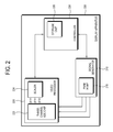
- FIG. 2 is a block diagram illustrating a configuration of a display apparatus according to an exemplary embodiment of the present invention
- FIGS. 3A and 3B are diagrams illustrating waveforms of R, G and B pattern signals, and Y, U and V pattern signals, respectively;
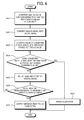
- FIG. 4 is a flowchart of performing calibration according to an exemplary embodiment of the present invention.
- FIG. 5 is a flowchart of performing calibration according to another exemplary embodiment of the present invention.
- FIG. 2 is a block diagram illustrating a configuration of a display apparatus according to an exemplary embodiment of the present invention.
- a display apparatus 200 may include, but is not limited to, a digital TV, a desktop computer, a notebook computer, a monitor, etc. Further, an electronic device may be used as the display apparatus 200 according to an exemplary embodiment of the present invention as long as it can display an image and perform analog to digital conversion (ADC).
- ADC analog to digital conversion
- the display apparatus 200 may include a signal generator 210, a video processor 220 and a controller 230.
- the signal generator 210 generates a signal.
- the signal generator 210 may generate an analog signal corresponding to a predetermined DC voltage.
- the predetermined DC voltage may include at least one of DC voltages representing black and white.
- the predetermined DC voltage may include at least one of 0.1V representing black and 0.6V representing white.
- the predetermined DC voltage may include at least one of a maximum voltage and a minimum voltage in a waveform of the analog signal.
- the predetermined DC voltage may include at least one of a minimum voltage of 0mV and a maximum voltage of 700mV.
- the signal generator 210 generates R, G and B pattern signals in the state that the display apparatus 200 operates in a PC mode, and generates Y, U and V pattern signals in the state that the display apparatus 200 operates in a DTV mode.
- the signal generator 210 may output the generated analog signal to the video processor 220.
- the signal generator 210 may generate an analog signal corresponding to a predetermined DC voltage by a pulse width modulation (PWM) method.
- the signal generator 210 may include a PWM port 215.
- the video processor 220 may perform calibration. Specifically, the video processor 220 converts the analog signal output from the signal generator 210 into a digital signal, and adjusts the digital signal to have the same value as a reference value. According to an exemplary embodiment of the present invention, the video processor 220 may adjust an offset and/or a gain of the digital signal on the basis of the analog signal corresponding to the DC voltage representing black and/or white.
- the video processor 220 may include a three-channel ADC chip 222 and a scaler 224.
- the three-channel ADC chip 222 converts the analog signals input according to channels into 8-bit digital signals having values of 0 ⁇ 255.
- the values of the converted digital signals may be stored in an internal register (not shown) of the scaler 224.
- the scaler 224 adjusts the values stored in the internal register to be equal to the reference value.
- the video processor 220 finishes the calibration when the value of the digital signal is equal to the reference value, but performs the calibration again if the value of the digital signal is not equal to the reference value.
- the video processor 220 may output a message of failed calibration if the calibration is performed equal to or more than a preset number of times.
- This message may be output in the form of at least one of an on screen display (OSD) and a voice.
- OSD on screen display
- the video processor 220 may be provided by, for example, but not limited to, a liquid crystal display (LCD), an organic light emitting diode (OLED), a plasma display panel (PDP), etc.
- LCD liquid crystal display
- OLED organic light emitting diode
- PDP plasma display panel
- the controller 230 may control the signal generator 210 to generate the analog signal corresponding to a predetermined DC voltage when performing the calibration.
- the controller 230 controls the signal generator 210 to generate the R, G and B pattern signals when the display apparatus 200 operates in the PC mode, and the Y, U and V pattern signals when the display apparatus 200 operates in the DTV mode.
- the controller 230 may control the video processor 220 to convert the analog signal generated by the signal generator 210 into the digital signal and to adjust the digital signal to have the same value as the reference value. Specifically, the controller 230 compares the reference value stored in a storage unit 235 with the value of the converted digital signal stored in the internal register of the scaler 224. Then, the controller 230 controls the video processor 220 to adjust the converted digital signal to have the same value as the reference value.
- the reference values may be set with values obtained by converting the analog signals corresponding to the DC voltages representing black and white into the digital values.
- the reference values may be set by a value (e.g., 0X01) obtained by converting 0.1V representing black into a digital value, and a value (e.g., 0X06) obtained by converting 0.6V representing white into a digital signal.
- the controller 230 may control the video processor 220 to adjust the gain and/or the offset of the digital signal on the basis of the analog signal corresponding to the DC voltage representing black and/or white.
- the reference values may be set with values obtained by converting the minimum and maximum voltages in the waveform of the analog signal into the digital signals.
- the reference values may be set by a value (e.g., 0X00) obtained by converting the minimum voltage of 0mV into a digital signal, and a value (e.g., 0X67) obtained by converting the maximum voltage of 700mV into a digital signal.
- controller 230 may control the video processor 220 to finish the calibration when the digital signal is adjusted to have the same value as the reference value, but perform the calibration again if the digital signal is adjusted not to have the same value as the reference value.
- controller 230 may control the video processor 220 to output a message of failed calibration if the calibration is performed equal to or more than a preset number of times.
- FIG. 3A is a diagram illustrating waveforms of R, G and B pattern signals and FIG. 3B is a diagram illustrating Y, U and V pattern signals.
- the R, G and B pattern signals have a level of 0mV ⁇ 700mV with respect to the ground, and this level is used in performing the calibration.
- the Y pattern signal has a level of 0mV ⁇ 700mV with respect to the ground, and this level is used in performing the calibration.
- the U and V pattern signals have an intermediate level (128 digital) of 350mV, and this level is used in performing the calibration.
- the calibration is independently performed in the PC mode and the DTV mode.
- FIG. 4 is a flowchart of performing calibration according to an exemplary embodiment of the present invention.
- a predetermined DC voltage generated by the signal generator 210 may include at least one of DC voltages representing black and white.
- the reference value previously set to adjust the gain and the offset may be set with a value obtained by converting an analog signal corresponding to the DC voltage representing black and white into a digital signal.
- the display apparatus 200 generates an analog signal corresponding to the DC voltages representing black and/or white in order to perform the calibration (S401). For example, the display apparatus 200 may output the DC level of 0.1V representing black and the DC level of 0.6V representing white through the PWM port. The display apparatus 200 converts the generated analog signal into the digital signal (S402).
- the display apparatus 200 compares the value of the converted digital signal with the previously stored reference value (S403).
- the previously stored reference value may be set with a value (e.g., 0X01) obtained by converting 0.1V representing black into a digital signal and with a value (e.g., 0X06) obtained by converting 0.6V representing white into a digital signal.
- the display apparatus 200 determines whether the value of the converted digital signal is equal to the previously stored reference value (S404). If it is determined that the value of the converted digital signal is equal to the previously stored reference value (S404-Y), the display apparatus 200 finishes the calibration (S408). In this case, the display apparatus 200 outputs a message of completed calibration, and informs a user that the calibration is successful.
- the display apparatus 200 adjusts the gain and the offset of the digital signal (S405).
- the display apparatus 200 adjusts a digital code converted from 0.1V representing black to be equal to the reference value.
- the display apparatus 200 adjusts the digital code converted from 0.1V representing black and the digital code converted from 0.6V representing white to be equal to the reference value.
- the display apparatus 200 determines whether the calibration is repeated equal to or more than a predetermined number of times (S406). If it is determined that the calibration is repeated equal to or more than a predetermined number of times (S406-Y), the display apparatus 200 outputs a message of failed calibration in the form of the OSD (S407). In this case, the message of the failed calibration may be output together with a circuit board check message.
- the display apparatus 200 If it is determined that the calibration is repeated less than a predetermined number of times (S406-N), the display apparatus 200 returns to the operation S404, thereby repetitively performing the calibration.
- the display apparatus internally and directly generates an analog signal corresponding to a predetermined DC voltage, thereby performing the calibration. Accordingly, the display apparatus can perform the calibration by itself even through it does not store any certain pattern for the calibration.
- FIG. 5 is a flowchart of performing calibration according to another exemplary embodiment of the present invention.
- a predetermined DC voltage generated by the signal generator 210 may include at least one of a minimum voltage and a maximum voltage in the waveform of the analog signal.
- a reference value previously set to adjust gain and offset may be set with a value obtained by converting the minimum and maximum voltages in the waveform of the analog signal into a digital signal.
- the display apparatus 200 generates an analog signal corresponding to the minimum voltage and/or the maximum voltage in the waveform of the analog signal so as to perform the calibration (S501). For example, the display apparatus 200 may output a minimum DC voltage of 0mV and a maximum DC voltage of 700mV through the PWM port.
- the display apparatus 200 converts the generated analog signal into the digital signal (S502).
- the display apparatus 200 compares the value of the converted digital signal with the previously stored reference value (S503)
- the previously stored reference value may be set with a value (e.g., 0X00) obtained by converting the minimum voltage of 0mV into a digital signal and with a value (e.g., 0X67) obtained by converting the maximum voltage of 700mV into a digital signal.
- the display apparatus 200 adjusts the gain and the offset of the digital signal (S505).
- the display apparatus 200 adjusts a digital code converted from the minimum voltage of 0mV to be equal to the reference value.
- the display apparatus 200 adjusts the digital code converted from the minimum voltage of 0mV and the digital code converted from the maximum voltage of 700mV to be equal to the reference values, respectively.
- HDMI high definition multimedia interface
- PC PC/component(Comp)/audio & video (AV) signals or the like.
- the display can perform the calibration by itself at its initial operation, and there is no separate process of connecting calibration lines.
Landscapes
- Engineering & Computer Science (AREA)
- Multimedia (AREA)
- Signal Processing (AREA)
- Health & Medical Sciences (AREA)
- Biomedical Technology (AREA)
- General Health & Medical Sciences (AREA)
- Control Of Indicators Other Than Cathode Ray Tubes (AREA)
- Controls And Circuits For Display Device (AREA)
Applications Claiming Priority (1)
| Application Number | Priority Date | Filing Date | Title |
|---|---|---|---|
| KR1020090051594A KR20100132815A (ko) | 2009-06-10 | 2009-06-10 | 디스플레이 장치 및 디스플레이 방법 |
Publications (2)
| Publication Number | Publication Date |
|---|---|
| EP2262274A2 true EP2262274A2 (de) | 2010-12-15 |
| EP2262274A3 EP2262274A3 (de) | 2012-11-21 |
Family
ID=42313958
Family Applications (1)
| Application Number | Title | Priority Date | Filing Date |
|---|---|---|---|
| EP10153747A Withdrawn EP2262274A3 (de) | 2009-06-10 | 2010-02-16 | Anzeigevorrichtung und Verfahren |
Country Status (3)
| Country | Link |
|---|---|
| US (1) | US20100315397A1 (de) |
| EP (1) | EP2262274A3 (de) |
| KR (1) | KR20100132815A (de) |
Family Cites Families (9)
| Publication number | Priority date | Publication date | Assignee | Title |
|---|---|---|---|---|
| US5371552A (en) * | 1991-10-31 | 1994-12-06 | North American Philips Corporation | Clamping circuit with offset compensation for analog-to-digital converters |
| DE4215668C2 (de) * | 1992-05-13 | 2003-06-12 | Thomson Brandt Gmbh | Klemmschaltung für ein digitales Videosignal |
| JP3428287B2 (ja) * | 1996-04-12 | 2003-07-22 | ソニー株式会社 | クランプ回路およびそれを用いた撮像装置 |
| KR100199878B1 (ko) * | 1996-08-31 | 1999-06-15 | 전주범 | Osd(on-screen display)신호처리장치와 그 방법 |
| JP2002344771A (ja) * | 2001-05-11 | 2002-11-29 | Alps Electric Co Ltd | 画像信号処理装置及び画像表示装置 |
| JP4259046B2 (ja) * | 2002-06-20 | 2009-04-30 | セイコーエプソン株式会社 | 画像表示装置および画像処理装置 |
| KR100514749B1 (ko) * | 2003-05-21 | 2005-09-14 | 삼성전자주식회사 | 디스플레이 기기의 자동 캘리브레이션 장치 및 방법 |
| TWI328401B (en) * | 2006-02-22 | 2010-08-01 | Novatek Microelectronics Corp | Apparatus and method for gain adjustment for analog ypbpr signals |
| TWI314424B (en) * | 2006-06-23 | 2009-09-01 | Marketech Int Corp | System and method for image signal contrast adjustment and overflow compensation |
-
2009
- 2009-06-10 KR KR1020090051594A patent/KR20100132815A/ko not_active Ceased
- 2009-12-29 US US12/648,875 patent/US20100315397A1/en not_active Abandoned
-
2010
- 2010-02-16 EP EP10153747A patent/EP2262274A3/de not_active Withdrawn
Non-Patent Citations (1)
| Title |
|---|
| None |
Also Published As
| Publication number | Publication date |
|---|---|
| US20100315397A1 (en) | 2010-12-16 |
| KR20100132815A (ko) | 2010-12-20 |
| EP2262274A3 (de) | 2012-11-21 |
Similar Documents
| Publication | Publication Date | Title |
|---|---|---|
| US10565936B2 (en) | Organic light emitting display device and the method for driving the same | |
| CN101667416B (zh) | 显示器的色温与gamma调整方法 | |
| US9966039B2 (en) | Method and device for modulating image display quality of display device among different gray levels | |
| US20080309766A1 (en) | Color calibrating method for setting target gamma curves of target display device | |
| CN108022565A (zh) | 调整方法以及显示器 | |
| JP2004280075A (ja) | 信号較正によるモニタ接続の補償 | |
| CN101132501A (zh) | 显示设备及其控制方法 | |
| US20050179639A1 (en) | Apparatus and method for simultaneously adjusting brightness and contrast of a display | |
| CN103383838A (zh) | 显示图像的装置和方法,驱动发光器件的装置和方法 | |
| KR102020283B1 (ko) | 디스플레이 장치의 휘도 제어 장치 및 방법, 디스플레이 장치 및 이의 구동 방법 | |
| KR20100124073A (ko) | 화상형성장치 및 그의 색상 보정 방법 그리고 그것을 이용한 출력 영상의 색상 보정을 위한 호스트 장치 | |
| EP2262274A2 (de) | Anzeigevorrichtung und Verfahren | |
| US8144075B2 (en) | Display system for outputting analog and digital signals to a plurality of display apparatuses, system and method | |
| KR100514749B1 (ko) | 디스플레이 기기의 자동 캘리브레이션 장치 및 방법 | |
| KR20170039817A (ko) | 표시 장치 및 이의 구동 방법 | |
| US10685607B2 (en) | Adjustment method for display de-Mura | |
| JP2008164850A (ja) | 液晶表示装置の基準電圧調整方法 | |
| KR101577228B1 (ko) | 영상 표시장치의 구동장치와 그 구동방법 | |
| TW201624453A (zh) | Lcd白平衡即時切換選擇之最佳化方法與系統 | |
| TWI458357B (zh) | 色彩分佈調整法與色彩分佈模組 | |
| US7646390B2 (en) | Display and display system | |
| KR20170015793A (ko) | 전원 공급부, 이를 포함하는 표시 장치, 및 이의 구동 방법 | |
| KR20230007063A (ko) | 디스플레이 장치, 디스플레이 신호의 노이즈 검출 회로, 및 노이즈 검출 방법 | |
| US12482437B2 (en) | Method and system for calculating adaptive panel color parameters | |
| KR101472586B1 (ko) | 영상표시기기의 전압 보정회로 및 그 방법 |
Legal Events
| Date | Code | Title | Description |
|---|---|---|---|
| PUAI | Public reference made under article 153(3) epc to a published international application that has entered the european phase |
Free format text: ORIGINAL CODE: 0009012 |
|
| AK | Designated contracting states |
Kind code of ref document: A2 Designated state(s): AT BE BG CH CY CZ DE DK EE ES FI FR GB GR HR HU IE IS IT LI LT LU LV MC MK MT NL NO PL PT RO SE SI SK SM TR |
|
| AX | Request for extension of the european patent |
Extension state: AL BA RS |
|
| RAP1 | Party data changed (applicant data changed or rights of an application transferred) |
Owner name: SAMSUNG ELECTRONICS CO., LTD. |
|
| PUAL | Search report despatched |
Free format text: ORIGINAL CODE: 0009013 |
|
| AK | Designated contracting states |
Kind code of ref document: A3 Designated state(s): AT BE BG CH CY CZ DE DK EE ES FI FR GB GR HR HU IE IS IT LI LT LU LV MC MK MT NL NO PL PT RO SE SI SK SM TR |
|
| AX | Request for extension of the european patent |
Extension state: AL BA RS |
|
| RIC1 | Information provided on ipc code assigned before grant |
Ipc: H04N 17/02 20060101ALI20121016BHEP Ipc: H04N 5/18 20060101ALI20121016BHEP Ipc: H04N 5/57 20060101ALI20121016BHEP Ipc: H04N 5/16 20060101AFI20121016BHEP |
|
| 17P | Request for examination filed |
Effective date: 20130424 |
|
| 17Q | First examination report despatched |
Effective date: 20140522 |
|
| STAA | Information on the status of an ep patent application or granted ep patent |
Free format text: STATUS: THE APPLICATION IS DEEMED TO BE WITHDRAWN |
|
| 18D | Application deemed to be withdrawn |
Effective date: 20150901 |