EP2263355B1 - Hochauflösender digitaler Modulator mit Umschaltung zwischen diskreten PWM- und PPM-Werten - Google Patents
Hochauflösender digitaler Modulator mit Umschaltung zwischen diskreten PWM- und PPM-Werten Download PDFInfo
- Publication number
- EP2263355B1 EP2263355B1 EP09727361A EP09727361A EP2263355B1 EP 2263355 B1 EP2263355 B1 EP 2263355B1 EP 09727361 A EP09727361 A EP 09727361A EP 09727361 A EP09727361 A EP 09727361A EP 2263355 B1 EP2263355 B1 EP 2263355B1
- Authority
- EP
- European Patent Office
- Prior art keywords
- symbol
- signal
- digital modulator
- waveform
- duty cycle
- Prior art date
- Legal status (The legal status is an assumption and is not a legal conclusion. Google has not performed a legal analysis and makes no representation as to the accuracy of the status listed.)
- Not-in-force
Links
Images



Classifications
-
- H—ELECTRICITY
- H04—ELECTRIC COMMUNICATION TECHNIQUE
- H04L—TRANSMISSION OF DIGITAL INFORMATION, e.g. TELEGRAPHIC COMMUNICATION
- H04L25/00—Baseband systems
- H04L25/38—Synchronous or start-stop systems, e.g. for Baudot code
- H04L25/40—Transmitting circuits; Receiving circuits
- H04L25/49—Transmitting circuits; Receiving circuits using code conversion at the transmitter; using predistortion; using insertion of idle bits for obtaining a desired frequency spectrum; using three or more amplitude levels ; Baseband coding techniques specific to data transmission systems
- H04L25/4902—Pulse width modulation; Pulse position modulation
Definitions
- the application relates to a digital modulator comprising an input terminal and a symbol generating unit. Moreover, the application relates to a transmitter comprising the digital modulator, a method and a computer readable medium having a computer program stored thereon for generating a modulated output signal.
- Transmitters are widely used in several application areas, like mobile radio or satellite technology. It is important for systems of such technology areas that energy consumption is small due to the limited power supply. Thus, it is an ongoing concern of the industry to reduce power consumption of transmitters.
- PWM pulse width modulation
- PPM pulse position modulation
- PDM pulse density modulation
- a switching power amplifier can be driven via its supply voltage, wherein the supply voltage may depend on the amplitude component.
- Another prior art solution for driving the switching power amplifier is to use a two-level PWM signal, which can be generated by comparing the amplitude modulated carrier signal and the phase modulated carrier signal with a saw tooth signal having a fundamental frequency of at least twice the carrier frequency.
- a further prior art modulation type may use a two-level PDM signal, which can be generated by a band-pass sigma-delta. All these solutions comprise an analogue circuitry. However, digital modulation may be desirable.
- a suitable solution may be to convert a complex signal to a phase modulated signal comprising a constant envelope.
- Such signals can be produced by pre-distorting four base band signals.
- an analogue circuitry is required and matching requirements may be high.
- a digital realization may comprise the drawback of extremely high sampling frequencies for achieving a desired resolution.
- a digital modulator comprising at least one input terminal configured to receive at least one signal.
- the invention is defined by the independent claims. Dependent claims describe advantageous embodiments.
- the digital modulator according to the present application can be employed within several transmitting devices for transmitting any kind of information, like data, speech or the like, to a suitable counterpart station.
- the transmitting devices can be preferably used in wireless communication systems.
- the digital modulator may comprise at least one input terminal for receiving at least a first signal. It is also possible that the digital modulator comprises more than one input terminal for receiving more than one input signal.
- the received signal may be a base band signal comprising at least parts of the information being transmitted. This signal may be generated by any kind of a signal generator.
- the needed sample frequency required for performing digital modulation to meet a desired resolution can be significantly reduced in case two symbol waveforms are generated and adaptive switching between these two symbol waveforms is performed.
- the symbol generating unit may be configured to generate two symbol waveforms depending on the received signal.
- the symbol waveforms can be generated at the same time. However, these symbol waveforms do not comprise the desired accuracy, which may depend on a desired resolution or dynamic range of the digital modulator.
- two coarse symbol waveforms can be generated comprising a different parameter value.
- a particular symbol waveform is characterized by at least one particular parameter value.
- Each symbol being transmitted comprises a different symbol waveform, and thus, a different parameter value.
- the parameter value may be an indicator for the measure of the quality of the desired modulated signal.
- both coarse symbol waveforms can be adaptively switched by the switching unit.
- the output terminal of the digital modulator may be connected to each output terminal of the generating unit for a particular time period to achieve the desired modulated signal with a high accuracy.
- the received signal may be a first quantized signal depending on an envelope component being transmitted and/or a phase component being transmitted.
- the information being transmitted can be represented by the envelope component as well as by the phase component of a signal.
- the present application provides for using both components resulting in a high flexibility and high data rate.
- the parameter value may be the duty cycle and/or phase and phase shift respectively.
- a quantized amplitude can be converted into a quantized duty cycle in an easy manner.
- the quantized amplitude may be related to the quantized duty cycle via the arc tan-function. Similar, the phase component can be converted.
- the symbol generating unit may be configured, for example to generate the first symbol waveform comprising a higher parameter value than the desired symbol waveform, and the second symbol waveform comprising a lower parameter value than the desired symbol waveform. It may be advantageous, in case both coarse symbol waveforms are adjacent to each other.
- the modulating signal can be determined by averaging the two symbol waveforms.
- the desired modulated signal may comprise a duty cycle, which is higher or lower compared to the first or second duty cycle, and thus, the average duty cycle may be the wanted duty cycle providing high accuracy of the signal.
- the symbol generating unit may be configured to generate a pulse width modulated symbol waveform and/or a pulse position modulated symbol waveform. Both symbol waveforms are especially suitable due to their constant envelope.
- the characterizing parameter value of the pulse width modulated symbol waveform may be the duty cycle, while the characterizing parameter value of the pulse position modulated symbol waveform may be the phase.
- the digital modulator may comprise a clock generator configured to generate a first clock signal, wherein the first clock signal may depend at least on the dynamic range of the digital modulator.
- the clock generator may generate a clock signal comprising a sample frequency, which is high enough to meet the requirements for achieving a desired resolution of the present digital modulator.
- the first clock signal may be provided for driving the symbol generating unit.
- at least the symbol generating unit may be configured to be controllable depending on the first clock signal.
- this sample frequency may be not high enough for directly generating an modulated output signal comprising the desired high accuracy.
- the digital modulator may for example further comprise a first dividing unit configured to generate a second clock signal depending on the first clock signal and a first dividing factor.
- the second clock signal may comprise a reduced frequency.
- the first dividing factor may depend on the maximum duty cycle and the maximum number of quantization levels. In other words, the dividing factor may represent the number of sample points within one symbol period.
- At least the controlling unit may be configured to be controllable depending on the second clock signal according to a further embodiment.
- the required clock frequency for driving the controlling unit is significantly reduced due to the need of merely one sample point during one symbol period.
- the digital modulator may comprise at least one second dividing unit configured to generate a third clock signal depending on the second clock signal and a second dividing factor.
- at least one delay unit may be configured to be controllable depending on the third clock signal.
- the incoming signal can be delayed by at least one symbol period resulting in that instead of the actual symbol applied at the input terminal of the digital signal, the previous received symbol value can be processed.
- Further delay units can be also employed. It may be possible that the delay units can be driven by an additional clock generator. However, the employment of a second divider instead of an additional clock generator may reduce the implementation effort.
- the symbol generating unit may for example comprise at least one symbol table provided for determining the first symbol waveform and/or the second symbol waveform depending on the received signal.
- the symbol generating unit may comprise a storage provided for recording the symbol table.
- the possible values of the received signal may be associated with at least one symbol waveform.
- the first symbol waveform can be directly determined, while the second symbol waveform can be determined using predefined rules or the like.
- the present application proposes to use merely parts of the received signal as address signal.
- the at least one symbol table can be provided for determining the first symbol waveform and/or the second symbol waveform depending on at least the most significant bit (MSB) of the quantized signal.
- MSB most significant bit
- more than one MSB bit can be used as address signal.
- the controlling unit may be configured to control the switching unit depending on at least the least significant bit (LSB) of the quantized signal.
- LSB least significant bit
- the received signal comprising a particular number of bits can be divided into MSB bits and LSB bits, wherein the actual division of the received signal may depend on the number of bits and/or further criteria, like the desired accuracy.
- the switching periods can be determined by using respective stored tables, wherein the switching periods are stored associated to the LSB bits. Thereby, switching period means the time a particular output terminal of the generating unit is connected to the this output terminal of the digital modulator.
- the controlling unit can be formed as a sigma delta modulator.
- a sigma delta modulator may comprise the advantage that the output signal pattern can be used in a simple manner for controlling the switching unit. More particularly, the ratio of the time period in which communication between a particular output terminal of the symbol generating unit and the output terminal of the digital modulator is established can be performed in a simple manner.
- the digital modulator may comprise a sequence controlling unit, wherein the sequence controlling unit may be configured to control the sequence of communication establishing of the switching unit depending on the current received signal and/or the next received signal.
- the sequence controlling unit may be configured to control the sequence of communication establishing of the switching unit depending on the current received signal and/or the next received signal.
- the power efficiency of the digital modulator can be improved by suitable power control.
- the digital modulator may comprise a power controlling unit, wherein the power controlling unit may be configured to control the selection of at least two symbol generating units. It is found that changing the duty cycle by changing the symbol generating units for phase signals, the power efficiency of the present digital modulator can be increased. For example, automatic gain control can be used for extra power control.
- a transmitter comprising a digital modulator as stated above.
- a transmitter may comprise, according to further variants of the application, more than one digital modulator.
- the transmitter may comprise two phase modulator, two envelope modulators or a combination of them.
- the use of more than one digital modulator may increase the data rate of the transmitter.
- the transmitter may comprise at least one amplifying unit. It may be possible that for each implemented digital modulator at least one amplifying unit can be arranged.
- the amplifying unit can be implemented as a switching power amplifying unit within the transmitter for reducing power consumption.
- a switching amplifying unit may encompass at least one input for the signal being amplified and at least one input for voltage supply.
- Such a switching unit can be employed in combination with suitable modulation methods, like pulse width modulation (PWM).
- PWM pulse width modulation
- the switching power amplifier may be a class D or class E amplifier. These types of power amplifiers are especially suitable due to their small power consumption.
- similar amplifying devices can also be implemented into the transmitter according to the application.
- the present transmitter according to embodiments may provide for a significant power consumption reduction.
- the transmitter may be formed as a switched linear amplification with non-linear components (LINC) transmitter.
- LINC transmitting concepts may comprise at least two digital modulators according to the present application.
- LINC transmitter provides for reduced power consumption and increased data rates.
- Another aspect of the present application is a method for generating a modulated output signal, comprising receiving at least one signal, generating a first symbol waveform depending on the received signal, generating at least a second symbol waveform depending on the received signal, wherein the first symbol waveform comprises at least one different parameter value compared to the second symbol waveform, and generating the modulated output signal by switching a third output terminal to at least the first symbol waveform and/or the symbol second waveform, wherein switching is controlled depending on the received signal.
- a further aspect of the present application is a computer readable medium having a computer program stored thereon.
- the computer program comprises instructions operable to cause a processor to perform at least the above stated method.
- the present application can be deployed in several application areas which include efficient modulated transmitters.
- the transmitters can be used for WLAN, WPAN, Bluetooth, OFDM, GSM, UMTS, CDMA, low power mobile communication devices and the like.
- example embodiments of the present application will describe and point out a digital modulator or transmitter having a digital modulator comprising a reduced sample rate and high dynamic range.
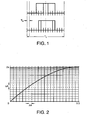
- Fig. 1 shows a diagram comprising an exemplified symbol pulse width modulated waveform and symbol pulse position modulated waveform. More particularly, the upper symbol waveforms depicted in Fig. 1 represent two possible PWM symbol waveforms and the lower symbol waveforms represent two possible PPM symbol waveforms. The depicted symbol waveforms are formed as ideal rectangular waveforms.
- N E represents the number of minimal step size T S .
- the PWM waveform differs from the PPM waveform in that the centre may not change as a function of the duty cycle d variation.
- the PWM waveform is symmetrical while the PPM waveform may be unsymmetrical.
- the minimal resolution ⁇ d can be determined by the ratio of T S and T C . Since the resolution is limited, the resolution of the amplitude component or phase component is also limited. For simplicity reasons, the following derivations depend on the amplitude component and PWM symbols. It shall be understood that the derivations may be similar with respect to the phase component and PPM symbols.
- d max 0.5.
- the dynamic range in particular the desired dynamic range, may be related to the maximum number of quantization levels L max .
- the maximum number of quantization levels L max can be calculated depending on the desired dynamic range. For calculating, a linear relation can be assumed. By way of example, for a desired a dynamic range of 50dB or approximately 8 bits, the maximum number of quantization levels L max must be 256 representing 256 quantization levels.
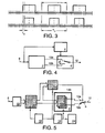
- FIG. 2 shows a further diagram comprising the ratio of an exemplified quantized envelope signal A n and quantized duty cycle d n .
- Fig. 3 shows a further diagram comprising the first symbol pulse width modulated waveform and the second pulse width modulated waveform. Shown are exemplified streams of the first symbol PWM waveform and the second symbol PWM waveform.
- a first simplified embodiment of the digital modulator according to the present application is shown.
- the shown digital modulator comprises an input terminal 8. Via the input terminal 8, the digital modulator may receive a digital signal.
- the digital signal can be generated by a suitable signal generator (not shown) depending on the information being transmitted.
- the digital signal can be fed to an arranged symbol generating unit 2.
- the symbol generating unit 2 may be a suitable generator for generating a PWM pulse, PPM pulse or the like. Furthermore, the symbol generating unit 2 comprises a first output terminal 10a and a second output terminal 10b.
- the two output terminals 10a and 10b of the symbol generating unit 2 are connected to a switching unit 6.
- the switching unit 6 may be a suitable switch.
- the switching unit can be controlled by a controlling unit 4.
- the controlling unit 4 comprises a communication to the input terminal 8.
- a third output terminal 12 is arranged at the switching unit 6.
- the third output terminal 12 may be provided for forwarding the desired modulated output signal to further processing units, like power amplifiers or the like (not shown). A detailed elucidation of the functioning of the present digital modulator occurs subsequently.
- Fig. 5 shows a second simplified embodiment of the digital modulator according to the present application.
- the shown embodiment comprises more details than the previous embodiment.
- the depicted digital modulator comprises a converting unit 22.
- the converting unit may be configured to convert a quantized input signal, like a quantized envelope signal A n+1 , to a suitable quantized signal for further processing, like a quantized duty cycle signal d n+1 , according to equation 1.8:
- the quantized signal such as the quantized duty cycle signal d n+1
- the quantized signal can be forwarded to a delay unit 20.
- the resulting signal like the delayed quantized duty cycle signal d n can be divided into two components, wherein one component may represent the LSB bits of d n and the other component may represent the MSB bits of d n .
- the MSB bits can be fed to the symbol generating unit 2, while the LSB bits can be forwarded to the controlling unit 4.
- the symbol generating unit 2 comprises two symbol tables 14a and 14b.
- the possible symbol waveforms can be recorded, wherein each symbol waveform can be associated to a particular value of the received MSB bits.
- each of the symbol tables14a and 14b can be connected to a respective output terminal 10a and 10b indicating that one symbol table 14a is used for generating the first symbol waveform and the other symbol table 14b is used for generating the second symbol waveform.
- merely one symbol table or a plurality of symbol tables can be arranged as well as the symbol tables may be identical or different to each other.
- the LSB bits are forwarded to the controlling unit 4.
- the controlling unit 4 can be configured to control the switching unit 6 depending on the LSB bits.
- the digital modulator comprises a clock circuit.
- the digital modulator comprises a clock generator 24, like any suitable clock generator.
- the clock generator 24 may generate a first sample frequency f S being directly used for driving the symbol generating unit 2.
- a suitable first dividing unit 16 comprising a first dividing factor N e is arranged.
- the second clock signal comprising a reduced frequency f C representing the carrier frequency can be used for driving the controlling unit 4.
- the second clock signal can be divided by a dividing factor M using the arranged second dividing unit 18 for generating a third clock signal comprising a reduced frequency f P .
- the provided delay unit 20 can be driven by this clock signal.
- more than one clock generator can be arranged. For instance, for each required clock signal, a respective clock generator can be arranged.
- Fig. 6 shows an exemplified flowchart of the method according to the present application.
- a signal in particular a digital signal is received by the digital modulator via input terminal 8 in step 104.
- the digital signal may be generated by a signal generator depending on the information being transmitted and may be a quantized envelope signal or phase signal.
- the method of the present application is merely elucidated with respect to an envelope signal. However, it shall be understood that similar steps may also apply for a phase signal.
- the quantized envelope signal A n+1 can be converted by the converting unit 22 to a quantized duty cycle signal d n+1 .
- a suitable processing device may perform converting using equation 1.8.
- the quantized duty cycle signal d n+1 can be delayed by a suitable delay unit 22 to achieve the quantized duty cycle signal d n in step 108. This can be performed depending on the third clock signal comprising a frequency f P less than the sample frequency f S .
- the obtained quantized duty cycle signal d n can be divided into LSB bits and MSB bits.
- the LSB bits can be forwarded to the controlling unit 4, while the MSB bits can be fed to the symbol generating unit 2. Forwarding the respective bits of the quantized duty cycle signal d n can be performed parallel.
- the symbol generating unit 2 is configured to select at least two symbol waveforms comprising coarse parameter values, in particular coarse duty cycles d ⁇ l , and d ⁇ l +1 , wherein the symbol waveforms may be PWM symbol waveforms, depending on the received MSB bits of the quantized duty cycle signal d n in step 110.
- the symbol generating unit 2 may comprise two symbol tables 14a and 14b, wherein each symbol table 14a, 14b includes particular symbol waveforms comprising coarse duty cycles d ⁇ l each associated to particular values of the received MSB bits.
- the recorded symbol waveforms within the symbol tables 14a and 14b are merely symbol waveforms comprising coarse duty cycles d ⁇ l , which do not comprises the required accuracy for the desired dynamic range.
- two adjacent coarse symbol waveforms comprising two adjacent duty cycles d ⁇ l and d ⁇ l +1 are determined. More particularly, at a time instance nT P the sampled envelope or duty cycle value may be forming an address signal d n from which the MSB bits are used to select two basic adjacent coarse waveforms d ⁇ l and d ⁇ l +1 in the symbol table 14a, 14b.
- Fig. 7 shows a further diagram comprising the duty cycles of the first symbol pulse width modulated waveform and the second pulse width modulated waveform.
- the duty cycle d[n] of the desired output signal is located between two adjacent coarse waveforms d ⁇ l and d ⁇ l +1 .
- the next desired duty cycle d[n+1] is reached.
- both symbol waveforms comprising the duty cycles d ⁇ l and d ⁇ l +1 can be generated depending on the sample frequency f S and outputted via the first and second output terminal 10a and 10b by the symbol generating unit 2.
- the controlling unit 4 can also analyze the received LSB bits in step 114.
- the average duty cycle d n, av can be determined by means of adapting switching between both symbol waveforms having the duty cycles d ⁇ l and d ⁇ l +1 in step 118.
- the switching time point must be determined depending on the LSB bits by the controlling unit 4. In other words, the time period each switching unit 6 is closed to a particular output terminal 10a, 10b of the symbol generating unit 2 must be determined.
- the LSB bits of d n can be used for determining the time periods.
- the average symbol waveform can be obtained by closing switching unit 6 for the time N.T c to the first output terminal 10a, and next closing switching unit 6 for the remaining time period to the second output terminal 10b given by (M-N)T c .
- N can be determined depending on the LSB bits. More particularly, the LSB bits of d n will select a two-level waveform which may determine the time period the switching unit 6 is closed to a particular output terminal 10a, 10b of the symbol generating unit 2.
- Equation 1.10 can be simplified for a PWM pulse as well as for a PPM pulse.
- the average duty cycle d n,av is given by d n
- the average duty cycle d n,av is given by d n
- step 116 the controlling unit 4 may drive the switching unit 6 according to the obtained results.
- the switching unit 6 may switch respectively and output the desired average symbol waveform or desired modulated output signal in step 120 for further processing.
- Fig. 8 shows a third embodiment of the digital modulator according to the present application.
- the third embodiment of the digital modulator comprises additionally a further delay unit 26 and a sequence controlling unit 28.
- a clock generator and a converting unit are not depicted.
- the input signal d n+2 received via input terminal can be delayed by delay unit 26 comprising the same delay factor Tp as delay unit 20.
- the obtained signal d n+1 is fed to the further delay unit 20 as well as to the sequence controlling unit 28.
- the delayed signal d n is divided and forwarded according to the previous embodiment.
- the LSB bits of d n are also fed to the sequence controlling unit 28.
- the sequence controlling unit 28 may be configured to determine depending on the bits of d n+1 and d n , which output terminal 10a, 10b of the symbol generating unit 2 is at first connected to the third output terminal 12. More particularly, in case the ratio between M and N does not change, many ways for obtaining the average duty cycle d n,av are possible. However, it is found, according to the present application that the accuracy of the output signal can be further improved, when the transition is smoothed.
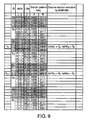
- FIG. 9 an exemplified table of a 5 bit quantized input signal is shown.
- the actually received duty cycles d n , d n+1 , etc. are depicted.
- the possible coarse symbol waveforms and their duty cycle d ⁇ l respectively are shown, while the following columns represent the five bits of the received signal divided into three MSB bits and two LSB bits. It shall be understood that, according to other variants of the present application, the division of the bits into MSB bits and LSB bits can be performed in other ways as well.
- the following columns are divided in A and B and represent switch pattern to get the wanted average duty cycle d n,av .
- the last column shows the coarse symbol selection by the MSB bits.
- the digital signal d n may comprise the value 01010.
- the MSB bits 010 can be fed to the symbol generating unit 2 and used to select the coarse symbol waveforms in the table.
- the MSB bits are associated to the duty cycle d ⁇ 2 .
- the first waveform may comprise the duty cycle d ⁇ 2 .
- the waveform comprising the duty cycle d ⁇ 3 can be selected. This can be performed by an additional symbol table, by predefined rules or the like.
- the switch pattern indicates the time period each output terminal 10a, 10b of the symbol generating unit 2 is connected to the third output terminal 12.
- Fig. 10 shows a fourth simplified embodiment of the digital modulator according to the present application.
- the present digital modulator differs from the previous embodiments in that a sigma delta modulator 30 is employed as controlling unit.
- the output signal pattern of the sigma delta modulator 30 can be next used to control the ratio of the time the switching unit 6 is closed to a particular output terminal 10a, 10b. It shall be understood that a further delay unit and a sequence controlling unit can also be employed within the present embodiment of the digital modulator.
- symbol waveforms with a variable duty cycle d symbol waveforms comprising a different phase F can be stored in the symbol tables.
- FIG. 11 An exemplified diagram comprising the first symbol pulse position modulated waveform and the second pulse position modulated waveform is shown in Fig. 11 .
- the present examples of two adjacent symbols shown in Fig. 11 may comprise different phase F.
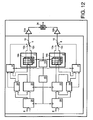
- Fig. 12 shows a first embodiment of the transmitter comprising the digital modulator according to the present application.
- the present transmitter is formed as a switched linear amplification with non-linear components (LINC) transmitter.
- the transmitter comprises two digital modulators, such as digital phase modulators, configured to generate phase modulated signals for a switched LINC transmitter.
- two amplifiers 32a and 32b are arranged for amplifying the output signals of the respective digital modulator to a suitable transmitting power.
- the two output signals can also be used to generate a PWM-PPM signal by addition of the two output signals using an adding unit 34.
- the input signals applied at input terminals 8 may be of the form ⁇ P [ n ] + ⁇ M [ n ] and ⁇ P [ n ] - ⁇ M [ n ], wherein index P represents the phase component and index M the magnitude component.
- Fig. 13 shows a second embodiment of the transmitter comprising the digital modulator according to the present application. For saving the simplicity of the embodiment in Fig. 13 , merely one digital modulator is shown in depth, while the further digital modulator is depicted by a rectangle 36. The further digital modulator may correspond to the digital modulator shown in depth.
- a plurality of symbol generating units 2, 2', 2" are arranged indicated by the dotted lines. Furthermore, a power controlling unit 38 is arranged.
- the power controlling unit 38 may be configured to select the most suitable generating unit 2, 2', 2". The power efficiency can be increased.
- an automatic gain control (AGC) can be implemented as power controlling unit 38.
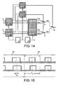
- Fig. 14 a third embodiment of the transmitter comprising the digital modulator according to the present application is shown.
- the shown embodiment uses the principles stated above for generating the wanted PWM-PPM signal
- the depicted transmitter comprises two input terminals 8 for receiving signals ⁇ P [ n +1] and d n+1 .
- the MSB bits of the duty cycle d[n] (envelope) and phase ⁇ P [n] can be used to select four symbol waveforms. Therefore, the symbol generating unit 2a may comprise four output terminals 10a to 10d.
- the chosen symbol waveforms for the duty cycle d and phase ⁇ may be the coarse representation of the desired duty cycle d and phase ⁇ .
- two switching units 6 are arranged for obtaining two symbol waveforms, like stream A and stream B, wherein these symbol waveforms stream A and stream B are more accurate.
- stream A may be applied, while at output terminal 12b, stream B may be applied.
- the average duty cycle d of both streams A and B may be equal and accurate, since the arranged switching units 6 are controlled depending on the LSB bits of signal d[n].
- streams A and B differs in their phase ⁇ .
- a further switching unit 40 is arranged, wherein the switching condition are given by N 2 * T C and M - N 2 * T C .
- the switching unit 40 is controlled depending on the LSB bits of signal ⁇ P [n] for obtaining besides the accurate duty cycle d also the accurate phase ⁇ .
- a further diagram shows the first symbol stream A and the second symbol stream B.
- the upper stream shown in Fig. 15 represents stream A, wherein stream A is the first or second symbol waveform
- the lower stream shown in Fig. 15 represents stream B, wherein stream B is the third or fourth symbol waveform.
- reference sign 42 indicates N 1 times first and third symbol waveforms
- reference sign 44 indicates (M-N 1 ) times second and fourth symbol waveforms.
- the logical blocks in the schematic block diagrams as well as the flowchart and algorithm steps presented in the above description may at least partially be implemented in electronic hardware and/or computer software, wherein it depends on the functionality of the logical block, flowchart step and algorithm step and on design constraints imposed on the respective devices to which degree a logical block, a flowchart step or algorithm step is implemented in hardware or software.
- the presented logical blocks, flowchart steps and algorithm steps may for instance be implemented in one or more digital signal processors, application specific integrated circuits, field programmable gate arrays or other programmable devices.
- the computer software may be stored in a variety of storage media of electric, magnetic, electro-magnetic or optic type and may be read and executed by a processor, such as for instance a microprocessor.
- a processor such as for instance a microprocessor.
- the processor and the storage medium may be coupled to interchange information, or the storage medium may be included in the processor.
Landscapes
- Physics & Mathematics (AREA)
- Spectroscopy & Molecular Physics (AREA)
- Engineering & Computer Science (AREA)
- Computer Networks & Wireless Communication (AREA)
- Signal Processing (AREA)
- Compression, Expansion, Code Conversion, And Decoders (AREA)
- Amplifiers (AREA)
Claims (14)
- Digitaler Modulator, welcher aufweist:zumindest ein Input-Terminal, welches konfiguriert ist, um zumindest ein Signal zu empfangen,eine Symbol-Generier-Einheit, welche ein erstens Output-Terminal und zumindest ein zweites Output-Terminal aufweist,wobei die Symbol-Generier-Einheit konfiguriert ist, abhängig von dem empfangenen Signal einer erstes Symbol Wellenform für das erste Output-Terminal zu generieren, undwobei die Symbol-Generier-Einheit konfiguriert ist, abhängig von dem empfangenen Signal zumindest eine zweites Symbol Wellenform für das zweite Output-Terminal zu generieren,wobei die erstes Symbol Wellenform zumindest einen unterschiedlichen Parameterwert verglichen mit der zweites Symbol Wellenform aufweist,zumindest ein drittes Output-Terminal, welches mit dem zumindest ersten Output-Terminal und/oder zweiten Output-Terminal mittels einer Schalteinheit verbindbar ist, undeine Steuereinheit, welche konfiguriert ist, die Schalteinheit abhängig von dem empfangenen Signal so zu steuern, dass ein moduliertes Output-Signal generiert wird, wobei der digitale Modulator dadurch gekennzeichnet ist, dass er ferner aufweisteine Sequenz-Steuereinheit, wobei die Sequenz-Steuereinheit konfiguriert ist, die Sequenz des Kommunikations-Herstellens der Schalteinheit zu steuern, abhängig von dem gegenwärtig empfangenen Signal und dem nächsten empfangenen Signal, zum Glätten eines Übergangs von einem Arbeitszyklus oder Phase in den nächsten Arbeitszyklus oder Phase mittels anfänglichem Schließens des Schalters mit einer ersten Klein-Grob-Arbeitszyklus Wellenform und folgendem Schließens des Schalters mit einem zweiten Groß-Grob-Arbeitszyklus Wellenform.
- Digitaler Modulator gemäß Anspruch 1, wobei das empfangene Signal ein erstes quanitisiertes Signal ist, welches abhängig ist von zumindest einer von:A) Amplituden-Komponente, welche übertragen wird,B) Phasen-Komponente, welche übertragen wird.
- Digitaler Modulator gemäß Anspruch 2, welcher ferner eine Verarbeitungseinheit aufweist, welche konfiguriert ist, die empfangene erste quantisierte Amplituden-Komponente und/oder Phasen-Komponente in ein zweites quantisiertes Signal zu konvertieren, welches den Parameterwert aufweist.
- Digitaler Modulator gemäß Anspruch 1, wobei die Symbol-Generier-Einheit konfiguriert ist, um zu generieren
die erstes Symbol Wellenform, welche einen höheren Parameterwert als das modulierte Output-Signal aufweist, und
die zweite Symbol Wellenform, welche einen niedrigeren Parameterwert als das modulierte Output-Signal aufweist. - Digitaler Modulator gemäß Anspruch 1, wobei die Symbol-Generier-Einheit konfiguriert ist, um zumindest eines von einer:A) puls-weiten-modulierte Symbol Wellenform,B) puls-phasen-modulierte Symbol Wellenform
zu generieren. - Digitaler Modulator gemäß Anspruch 1, welcher ferner aufweist
einen Taktgenerator, welcher konfiguriert ist, ein erstes Taktsignal zu generieren,
wobei das erste Taktsignal von zumindest dem dynamischen Bereich des digitalen Modulators abhängt. - Digitaler Modulator gemäß Anspruch 1, wobei die Symbol-Generier-Einheit zumindest eine Symboltabelle aufweist, welche zum Determinieren der erstes Symbol Wellenform und/oder der zweites Symbol Wellenform, abhängig von dem empfangenen Signal, bereitgestellt ist.
- Digitaler Modulator gemäß Anspruch 7, wobei die zumindest eine Symboltabelle zum Determinieren der erstes Symbol Wellenform und/oder der zweites Symbol Wellenform, abhängig von zumindest einem Bit höchster Wertigkeit des empfangenen Signals, bereitgestellt ist.
- Digitaler Modulator gemäß Anspruch 1, wobei die Steuereinheit zum Steuern der Schalteinheit, abhängig von zumindest einem Bit geringster Wertigkeit des empfangenen Signals, konfiguriert ist.
- Digitaler Modulator gemäß Anspruch 1, wobei die Steuereinheit als ein Sigma-Delta-Modulator ausgebildet ist.
- Digital Modulator gemäß Anspruch 1, welcher ferner aufweist eine Leistungs-Steuereinheit,
wobei die Leistungs-Steuereinheit konfiguriert ist, eine Selektion von zumindest zwei Generier-Einheiten zu steuern. - Transmitter, welcher einen digitalen Modulator gemäß Anspruch 1 aufweist.
- Verfahren zum Generieren eines modulierten Output-Signals, aufweisend:Empfangen zumindest eines Signals,Generieren einer erstes Symbol Wellenform abhängig von dem empfangenen Signal,Generieren zumindest einer zweites Symbol Wellenform abhängig von dem empfangenen Signal,wobei die erstes Symbol Wellenform zumindest einen unterschiedlichen Parameterwert verglichen mit der zweites Symbol Wellenform aufweist,Generieren des modulierten Output-Signals mittels Schalten eines dritten Output-Terminals zu zumindest der erstes Symbol Wellenform und/oder der zweites Symbol Wellenform, undwobei das Schalten abhängig von dem empfangenen Signal so gesteuert ist, dass das modulierte Output-Signal generiert wird,wobei das digitale Verfahren dadurch gekennzeichnet ist, dass es ferner aufweistSteuern des Schaltens abhängig von dem gegenwärtig empfangenen Signal und/oder dem nächsten empfangenen Signal zum Glätten eines Übergangs von einem Arbeitszyklus oder Phase in den nächsten Arbeitszyklus oder Phase mittels anfänglichem Schaltens zu einer ersten Klein-Grob-Arbeitszyklus Wellenform und folgendem Schaltens zu einem zweiten Groß-Grob-Arbeitszyklus Wellenform.
- Computer-lesbares Medium, welches ein darauf gespeichertes Computer-Programm hat, wobei das Computer-Programm aufweist:Instruktionen, welche funktionsfähig sind, einen Prozessor zu veranlassen das Verfahren gemäß Anspruch 13 auszuführen.
Priority Applications (1)
| Application Number | Priority Date | Filing Date | Title |
|---|---|---|---|
| EP09727361A EP2263355B1 (de) | 2008-03-31 | 2009-03-27 | Hochauflösender digitaler Modulator mit Umschaltung zwischen diskreten PWM- und PPM-Werten |
Applications Claiming Priority (3)
| Application Number | Priority Date | Filing Date | Title |
|---|---|---|---|
| EP08103182 | 2008-03-31 | ||
| PCT/IB2009/051288 WO2009122333A2 (en) | 2008-03-31 | 2009-03-27 | Digital modulator |
| EP09727361A EP2263355B1 (de) | 2008-03-31 | 2009-03-27 | Hochauflösender digitaler Modulator mit Umschaltung zwischen diskreten PWM- und PPM-Werten |
Publications (2)
| Publication Number | Publication Date |
|---|---|
| EP2263355A2 EP2263355A2 (de) | 2010-12-22 |
| EP2263355B1 true EP2263355B1 (de) | 2012-09-12 |
Family
ID=41112550
Family Applications (1)
| Application Number | Title | Priority Date | Filing Date |
|---|---|---|---|
| EP09727361A Not-in-force EP2263355B1 (de) | 2008-03-31 | 2009-03-27 | Hochauflösender digitaler Modulator mit Umschaltung zwischen diskreten PWM- und PPM-Werten |
Country Status (3)
| Country | Link |
|---|---|
| US (1) | US8416880B2 (de) |
| EP (1) | EP2263355B1 (de) |
| WO (1) | WO2009122333A2 (de) |
Cited By (1)
| Publication number | Priority date | Publication date | Assignee | Title |
|---|---|---|---|---|
| DE102016106790A1 (de) * | 2016-04-13 | 2017-10-19 | Forschungsverbund Berlin E.V. | Modulator für einen digitalen Verstärker |
Families Citing this family (26)
| Publication number | Priority date | Publication date | Assignee | Title |
|---|---|---|---|---|
| WO2010052668A1 (en) | 2008-11-10 | 2010-05-14 | Nxp B.V. | Variable duty cycle generation for out-phasing and pwm power amplifiers |
| US8554136B2 (en) | 2008-12-23 | 2013-10-08 | Waveconnex, Inc. | Tightly-coupled near-field communication-link connector-replacement chips |
| WO2012049669A1 (en) * | 2010-10-11 | 2012-04-19 | Dsp Group Ltd. | A method and circuit for increasing pwm resolution in digital controlled dc to dc converters |
| EP2689492B1 (de) | 2011-03-24 | 2020-01-08 | Keyssa, Inc. | Integrierte schaltung mit elektromagnetischer kommunikation |
| US9614590B2 (en) | 2011-05-12 | 2017-04-04 | Keyssa, Inc. | Scalable high-bandwidth connectivity |
| US8811526B2 (en) * | 2011-05-31 | 2014-08-19 | Keyssa, Inc. | Delta modulated low power EHF communication link |
| TWI569031B (zh) | 2011-06-15 | 2017-02-01 | 奇沙公司 | 使用ehf信號的近端感測與距離量測 |
| KR101879907B1 (ko) | 2011-09-15 | 2018-08-16 | 키사, 아이엔씨. | 유전체 매체와의 무선 통신 |
| US9705204B2 (en) | 2011-10-20 | 2017-07-11 | Keyssa, Inc. | Low-profile wireless connectors |
| TWI562555B (en) | 2011-10-21 | 2016-12-11 | Keyssa Inc | Contactless signal splicing |
| JP6435194B2 (ja) | 2011-12-14 | 2018-12-05 | ケッサ・インコーポレーテッド | 触覚フィードバックを提供するコネクタ |
| DE102011121139B4 (de) * | 2011-12-15 | 2016-11-24 | IAD Gesellschaft für Informatik, Automatisierung und Datenverarbeitung mbH | Vorrichtung mit einem Delta-Sigma-Modulator und einer mit diesem verbundenen MOSFET-Endstufe |
| US9559790B2 (en) | 2012-01-30 | 2017-01-31 | Keyssa, Inc. | Link emission control |
| US9344201B2 (en) | 2012-01-30 | 2016-05-17 | Keyssa, Inc. | Shielded EHF connector assemblies |
| CN107276641B (zh) | 2012-03-02 | 2021-07-02 | 凯萨股份有限公司 | 双工通信系统和方法 |
| US9515365B2 (en) | 2012-08-10 | 2016-12-06 | Keyssa, Inc. | Dielectric coupling systems for EHF communications |
| US9252995B2 (en) | 2012-08-27 | 2016-02-02 | Telefonaktiebolaget L M Ericsson (Publ) | Transmission of pulse length modulation information |
| EP2896135B1 (de) | 2012-09-14 | 2019-08-14 | Keyssa, Inc. | Drahtlose verbindungen mit virtueller hysterese |
| WO2014100058A1 (en) | 2012-12-17 | 2014-06-26 | Waveconnex, Inc. | Modular electronics |
| CN105556864B (zh) | 2013-03-15 | 2018-02-16 | 凯萨股份有限公司 | 非接触式ehf数据通信 |
| KR20150132459A (ko) | 2013-03-15 | 2015-11-25 | 키사, 아이엔씨. | Ehf 보안 통신 장치 |
| KR101886739B1 (ko) | 2013-03-15 | 2018-08-09 | 키사, 아이엔씨. | 극고주파 통신 칩 |
| US9166577B2 (en) * | 2014-01-29 | 2015-10-20 | Qualcomm Incorporated | Modulation through differentially delayed clocks |
| CN104061899B (zh) * | 2014-06-20 | 2016-03-30 | 东南大学 | 一种基于卡尔曼滤波的车辆侧倾角与俯仰角估计方法 |
| JP2018093399A (ja) * | 2016-12-05 | 2018-06-14 | 日本無線株式会社 | 高効率デジタル変調送信機 |
| WO2019134176A1 (zh) | 2018-01-08 | 2019-07-11 | 华为技术有限公司 | 一种相机通信方法及装置 |
Family Cites Families (58)
| Publication number | Priority date | Publication date | Assignee | Title |
|---|---|---|---|---|
| DE2324542C3 (de) * | 1973-05-15 | 1979-01-25 | Siemens Ag, 1000 Berlin Und 8000 Muenchen | Schaltungsanordnung zur frequenzdifferenziellen Phasenmodulation |
| US3896399A (en) * | 1973-07-19 | 1975-07-22 | Motorola Inc | Loop filter for delta modulator |
| US4155260A (en) * | 1978-05-24 | 1979-05-22 | General Electric Company | Ultrasonic imaging system |
| US4961204A (en) * | 1988-05-23 | 1990-10-02 | Hitachi, Ltd. | PCM signal generating/reproducing apparatus |
| CH689471A5 (de) * | 1994-05-05 | 1999-04-30 | Landis & Gyr Tech Innovat | Anordnung zum Summieren von Produkten zweier gleichen oder unterschiedlichen Signale. |
| US5463661A (en) * | 1995-02-23 | 1995-10-31 | Motorola, Inc. | TX preemphasis filter and TX power control based high speed two wire modem |
| US5589805A (en) * | 1995-11-06 | 1996-12-31 | General Motors Corporation | Enhanced resolution pulse width modulation control |
| US5731728A (en) * | 1995-11-13 | 1998-03-24 | National Semiconductor Corporation | Digital modulated clock circuit for reducing EMI spectral density |
| US5896101A (en) * | 1996-09-16 | 1999-04-20 | Audiologic Hearing Systems, L.P. | Wide dynamic range delta sigma A/D converter |
| JPH10117220A (ja) * | 1996-10-11 | 1998-05-06 | Hitachi Denshi Ltd | ディジタル復調器 |
| DE19646747C1 (de) * | 1996-11-01 | 1998-08-13 | Nanotron Ges Fuer Mikrotechnik | Verfahren zur drahtlosen Übertragung einer einem Signal aufgeprägten Nachricht |
| JP4014648B2 (ja) * | 1997-03-27 | 2007-11-28 | コーニンクレッカ フィリップス エレクトロニクス エヌ ヴィ | デジタル制御切換モード電圧変換器 |
| US6421396B1 (en) * | 1997-04-16 | 2002-07-16 | Broadcom Corporation | Variable rate modulator |
| JP4409743B2 (ja) * | 2000-02-25 | 2010-02-03 | パナソニック株式会社 | 無線通信装置及び無線通信方式 |
| US7176948B2 (en) * | 2000-04-12 | 2007-02-13 | Honeywell International Inc. | Method, apparatus and computer program product for controlling LED backlights and for improved pulse width modulation resolution |
| EP1178605A1 (de) * | 2000-07-19 | 2002-02-06 | Abb Research Ltd. | Verfahren und Vorrichtung zur Pulsbreitenmodulation |
| TW519792B (en) * | 2000-08-30 | 2003-02-01 | Cirrus Logic Inc | Circuits and methods for reducing interference from switched mode circuits |
| WO2002028126A1 (fr) * | 2000-08-31 | 2002-04-04 | Huawei Technologies Co., Ltd. | Procede de modulation par deplacement de 8 phases (8mdp) et dispositif associe |
| US6924681B2 (en) * | 2001-05-23 | 2005-08-02 | Texas Instruments Incorporated | Efficient pulse amplitude modulation transmit modulation |
| US6538484B1 (en) * | 2002-03-18 | 2003-03-25 | Lynx-Photonic Networks Ltd. | High-frequency PWM voltage control |
| US6765436B1 (en) * | 2002-09-04 | 2004-07-20 | Cirrus Logic, Inc. | Power supply based audio compression for digital audio amplifier |
| US6903619B2 (en) * | 2003-06-04 | 2005-06-07 | M/A-Com, Inc. | Electromagnetic wave transmitter systems, methods and articles of manufacture |
| US7164713B2 (en) * | 2002-12-24 | 2007-01-16 | Realtek Semiconductor Corp. | Interpolating root nyquist filter for variable rate modulator |
| TW589805B (en) * | 2003-01-30 | 2004-06-01 | Elan Microelectronics Corp | RF transmitter system of single quartz crystal oscillator |
| US7123890B2 (en) | 2003-03-11 | 2006-10-17 | Andrew Corporation | Signal sample acquisition techniques |
| US8593932B2 (en) * | 2003-05-16 | 2013-11-26 | Qualcomm Incorporated | Efficient signal transmission methods and apparatus using a shared transmission resource |
| JP2004345280A (ja) | 2003-05-23 | 2004-12-09 | Canon Inc | デジタルpwm信号生成回路 |
| WO2005012925A2 (en) * | 2003-06-19 | 2005-02-10 | Kernco, Inc. | Improved resource allocation technique |
| US8396111B2 (en) * | 2003-07-25 | 2013-03-12 | Powervation Limited | Digital pulse width modulator |
| US7688766B2 (en) * | 2003-09-17 | 2010-03-30 | Intel Corporation | Modulation scheme for orthogonal frequency division multiplexing systems or the like |
| KR100580177B1 (ko) * | 2003-09-22 | 2006-05-15 | 삼성전자주식회사 | 디지털 방송 수신 시스템에서 디스플레이 동기 신호 생성 장치 및 디코더와 그 방법 |
| US7515652B2 (en) * | 2003-09-30 | 2009-04-07 | Broadcom Corporation | Digital modulator for a GSM/GPRS/EDGE wireless polar RF transmitter |
| DE10355320B3 (de) * | 2003-11-27 | 2005-04-14 | Infineon Technologies Ag | Hochauflösender digitaler Pulsweitenmodulator und Verfahren zum Erzeugen eines hochaufgelösten pulsweitenmodulierten Signals |
| JP3858021B2 (ja) * | 2003-12-26 | 2006-12-13 | 松下電器産業株式会社 | 変調器、半導体集積回路、有線および無線通信装置 |
| CN100576740C (zh) * | 2004-03-10 | 2009-12-30 | 松下电器产业株式会社 | 数据转换器装置和数据转换方法及其发射机电路、通信装置和电子装置 |
| EP1743429A1 (de) * | 2004-04-09 | 2007-01-17 | Audioasics A/S | Sigma-delta-modulator |
| CN101902434A (zh) * | 2004-04-30 | 2010-12-01 | 夏普株式会社 | 无线通信系统 |
| US20060088081A1 (en) * | 2004-10-22 | 2006-04-27 | Time Domain Corporation | Transmit-rake apparatus in communication systems and associated methods |
| JP4560552B2 (ja) * | 2004-12-30 | 2010-10-13 | エージェンシー フォー サイエンス,テクノロジー アンド リサーチ | 完全集積化超広帯域送信機回路及びシステム |
| JP4116005B2 (ja) * | 2005-02-18 | 2008-07-09 | シャープ株式会社 | デルタシグマ変調器およびそれを用いたスイッチング増幅回路 |
| US7990840B2 (en) * | 2005-03-08 | 2011-08-02 | Qualcomm Incorporated | Methods and apparatus for efficient digital broadcast signaling in a wireless communications system |
| WO2006096678A1 (en) * | 2005-03-08 | 2006-09-14 | Qualcomm Flarion Technologies, Inc. | Transmission methods and apparatus combining pulse modulation and hierarchical modulation |
| US7804763B2 (en) * | 2005-04-04 | 2010-09-28 | Current Technologies, Llc | Power line communication device and method |
| FI20055229A0 (fi) * | 2005-05-16 | 2005-05-16 | Nokia Corp | Signaali-häiriö-tehosuhteen estimaattori |
| EP1900102A2 (de) * | 2005-06-27 | 2008-03-19 | Qualcomm Flarion Technologies, Inc. | Verfahren und vorrichtungen zum implementieren und/oder verwenden von verstärkern und/oder zum ausführen verschiedener verstärkungsbezogener operationen |
| US7417513B2 (en) * | 2005-08-17 | 2008-08-26 | M/A-Com, Inc. | System and method for signal filtering in a phase-locked loop system |
| JP4760909B2 (ja) | 2005-09-13 | 2011-08-31 | トヨタ自動車株式会社 | Pwm信号生成回路 |
| US7339427B2 (en) * | 2005-12-02 | 2008-03-04 | Sigc Semiconductor (Europe) Limited | Analogue power control in a saturated amplifier |
| US20110051763A1 (en) * | 2005-12-14 | 2011-03-03 | Kernco, Inc. | Determining and setting the frequency modulation index of a laser in a CPT frequency standard |
| KR100801034B1 (ko) * | 2006-02-07 | 2008-02-04 | 삼성전자주식회사 | 지연된 클럭 신호들을 이용하여 시그마-델타 변조시노이즈을 줄이는 방법과 이를 이용한 프랙셔널 분주 방식의위상고정루프 |
| KR101297710B1 (ko) * | 2006-08-10 | 2013-08-20 | 삼성전자주식회사 | 낮은 지터 스프레드 스펙트럼 클럭 발생기 |
| WO2008081876A1 (ja) * | 2006-12-28 | 2008-07-10 | Sharp Kabushiki Kaisha | 無線送信装置、制御装置、無線通信システムおよび通信方法 |
| JP2008251070A (ja) * | 2007-03-29 | 2008-10-16 | Hitachi Ltd | 半導体記憶装置 |
| US20080303565A1 (en) * | 2007-06-08 | 2008-12-11 | Yen-Hsun Hsu | Dll circuit and related method for avoiding stuck state and harmonic locking utilizing a frequency divider and an inverter |
| US8446849B2 (en) * | 2007-06-20 | 2013-05-21 | Qualcomm Incorporated | Methods and apparatuses for power control |
| US20090052568A1 (en) * | 2007-07-25 | 2009-02-26 | Oki Electric Industry Co., Ltd. | Qam communication system and method thereof and qam receiving apparatus and method thereof |
| KR20090060951A (ko) * | 2007-12-10 | 2009-06-15 | 한국전자통신연구원 | 단일 무선 채널에서 복수 스트림 병렬 전송을 위한 핸드쉐이크 방법, 전송전력 결정 방법 및 그 장치 |
| US8737925B2 (en) * | 2011-03-10 | 2014-05-27 | Comtech Ef Data Corp. | Method for the control of a wireless communications link for mitigating adjacent satellite interference |
-
2009
- 2009-03-27 EP EP09727361A patent/EP2263355B1/de not_active Not-in-force
- 2009-03-27 US US12/934,346 patent/US8416880B2/en not_active Expired - Fee Related
- 2009-03-27 WO PCT/IB2009/051288 patent/WO2009122333A2/en not_active Ceased
Cited By (2)
| Publication number | Priority date | Publication date | Assignee | Title |
|---|---|---|---|---|
| DE102016106790A1 (de) * | 2016-04-13 | 2017-10-19 | Forschungsverbund Berlin E.V. | Modulator für einen digitalen Verstärker |
| DE102016106790B4 (de) | 2016-04-13 | 2022-02-24 | Ferdinand-Braun-Institut gGmbH, Leibniz- Institut für Höchstfrequenztechnik | Modulator für einen digitalen Verstärker |
Also Published As
| Publication number | Publication date |
|---|---|
| EP2263355A2 (de) | 2010-12-22 |
| WO2009122333A2 (en) | 2009-10-08 |
| WO2009122333A3 (en) | 2010-02-11 |
| US20110044404A1 (en) | 2011-02-24 |
| US8416880B2 (en) | 2013-04-09 |
Similar Documents
| Publication | Publication Date | Title |
|---|---|---|
| EP2263355B1 (de) | Hochauflösender digitaler Modulator mit Umschaltung zwischen diskreten PWM- und PPM-Werten | |
| EP3219063B1 (de) | System und verfahren zur erzeugung eines mehrbandsignals | |
| US8489037B2 (en) | Power amplifying apparatus with bandwidth limitation processing on variable power supply | |
| US7058464B2 (en) | Device and method for signal processing | |
| EP2509218B1 (de) | System und Verfahren zur Erzeugung eines pulsbreitenmodulierten Signals | |
| US6429737B1 (en) | Method and apparatus for multi-channel digital amplification | |
| CN101427459A (zh) | 用于优化功率放大器效率的方法和布置 | |
| EP3679647B1 (de) | Dreiphasige modulation für effizienten und breitbandigen funksender | |
| US7932790B2 (en) | Switched modulation of a radio-frequency amplifier | |
| Hühn et al. | A new modulator for digital RF power amplifiers utilizing a wavetable approach | |
| US9258081B2 (en) | High dynamic range AMAM predistortion | |
| US8299866B2 (en) | Method and device including signal processing for pulse width modulation | |
| JP2008259201A (ja) | デジタル変調のためのシステム及び方法 | |
| US8792578B2 (en) | Method and apparatus of switched amplification having improved efficiency | |
| EP2733846B1 (de) | Hüllkurvenmodulator und Verfahren für den Betrieb eines Hüllkurvenmodulators | |
| CN103780262B (zh) | 差动式内插脉冲宽度调变数字模拟转换装置及方法 | |
| WO2008076233A1 (en) | Method and apparatus for a nonlinear feedback control system | |
| Adrian et al. | A review of design methods for digital modulators | |
| Chen et al. | An Equal-Area Criterion Based Pulse Encoding Strategy for RF Switch-Mode Power Amplifier. | |
| EP2728745B1 (de) | Signalmodulierung durch Impulsfolgensegmente für Funkfrequenzkommunikation |
Legal Events
| Date | Code | Title | Description |
|---|---|---|---|
| PUAI | Public reference made under article 153(3) epc to a published international application that has entered the european phase |
Free format text: ORIGINAL CODE: 0009012 |
|
| 17P | Request for examination filed |
Effective date: 20101102 |
|
| AK | Designated contracting states |
Kind code of ref document: A2 Designated state(s): AT BE BG CH CY CZ DE DK EE ES FI FR GB GR HR HU IE IS IT LI LT LU LV MC MK MT NL NO PL PT RO SE SI SK TR |
|
| DAX | Request for extension of the european patent (deleted) | ||
| GRAP | Despatch of communication of intention to grant a patent |
Free format text: ORIGINAL CODE: EPIDOSNIGR1 |
|
| RTI1 | Title (correction) |
Free format text: HIGH RESOLUTION DIGITAL MODULATOR BY SWITCHING BETWEEN DISCRETE PWM OR PPM VALUES |
|
| GRAS | Grant fee paid |
Free format text: ORIGINAL CODE: EPIDOSNIGR3 |
|
| GRAA | (expected) grant |
Free format text: ORIGINAL CODE: 0009210 |
|
| AK | Designated contracting states |
Kind code of ref document: B1 Designated state(s): AT BE BG CH CY CZ DE DK EE ES FI FR GB GR HR HU IE IS IT LI LT LU LV MC MK MT NL NO PL PT RO SE SI SK TR |
|
| REG | Reference to a national code |
Ref country code: GB Ref legal event code: FG4D |
|
| REG | Reference to a national code |
Ref country code: CH Ref legal event code: EP |
|
| REG | Reference to a national code |
Ref country code: AT Ref legal event code: REF Ref document number: 575469 Country of ref document: AT Kind code of ref document: T Effective date: 20120915 |
|
| REG | Reference to a national code |
Ref country code: IE Ref legal event code: FG4D |
|
| REG | Reference to a national code |
Ref country code: DE Ref legal event code: R096 Ref document number: 602009009719 Country of ref document: DE Effective date: 20121108 |
|
| PG25 | Lapsed in a contracting state [announced via postgrant information from national office to epo] |
Ref country code: NO Free format text: LAPSE BECAUSE OF FAILURE TO SUBMIT A TRANSLATION OF THE DESCRIPTION OR TO PAY THE FEE WITHIN THE PRESCRIBED TIME-LIMIT Effective date: 20121212 Ref country code: FI Free format text: LAPSE BECAUSE OF FAILURE TO SUBMIT A TRANSLATION OF THE DESCRIPTION OR TO PAY THE FEE WITHIN THE PRESCRIBED TIME-LIMIT Effective date: 20120912 Ref country code: LT Free format text: LAPSE BECAUSE OF FAILURE TO SUBMIT A TRANSLATION OF THE DESCRIPTION OR TO PAY THE FEE WITHIN THE PRESCRIBED TIME-LIMIT Effective date: 20120912 Ref country code: HR Free format text: LAPSE BECAUSE OF FAILURE TO SUBMIT A TRANSLATION OF THE DESCRIPTION OR TO PAY THE FEE WITHIN THE PRESCRIBED TIME-LIMIT Effective date: 20120912 |
|
| REG | Reference to a national code |
Ref country code: NL Ref legal event code: VDEP Effective date: 20120912 |
|
| REG | Reference to a national code |
Ref country code: AT Ref legal event code: MK05 Ref document number: 575469 Country of ref document: AT Kind code of ref document: T Effective date: 20120912 |
|
| REG | Reference to a national code |
Ref country code: LT Ref legal event code: MG4D Effective date: 20120912 |
|
| PG25 | Lapsed in a contracting state [announced via postgrant information from national office to epo] |
Ref country code: SE Free format text: LAPSE BECAUSE OF FAILURE TO SUBMIT A TRANSLATION OF THE DESCRIPTION OR TO PAY THE FEE WITHIN THE PRESCRIBED TIME-LIMIT Effective date: 20120912 Ref country code: GR Free format text: LAPSE BECAUSE OF FAILURE TO SUBMIT A TRANSLATION OF THE DESCRIPTION OR TO PAY THE FEE WITHIN THE PRESCRIBED TIME-LIMIT Effective date: 20121213 Ref country code: LV Free format text: LAPSE BECAUSE OF FAILURE TO SUBMIT A TRANSLATION OF THE DESCRIPTION OR TO PAY THE FEE WITHIN THE PRESCRIBED TIME-LIMIT Effective date: 20120912 Ref country code: SI Free format text: LAPSE BECAUSE OF FAILURE TO SUBMIT A TRANSLATION OF THE DESCRIPTION OR TO PAY THE FEE WITHIN THE PRESCRIBED TIME-LIMIT Effective date: 20120912 |
|
| PG25 | Lapsed in a contracting state [announced via postgrant information from national office to epo] |
Ref country code: IS Free format text: LAPSE BECAUSE OF FAILURE TO SUBMIT A TRANSLATION OF THE DESCRIPTION OR TO PAY THE FEE WITHIN THE PRESCRIBED TIME-LIMIT Effective date: 20130112 Ref country code: NL Free format text: LAPSE BECAUSE OF FAILURE TO SUBMIT A TRANSLATION OF THE DESCRIPTION OR TO PAY THE FEE WITHIN THE PRESCRIBED TIME-LIMIT Effective date: 20120912 Ref country code: ES Free format text: LAPSE BECAUSE OF FAILURE TO SUBMIT A TRANSLATION OF THE DESCRIPTION OR TO PAY THE FEE WITHIN THE PRESCRIBED TIME-LIMIT Effective date: 20121223 Ref country code: RO Free format text: LAPSE BECAUSE OF FAILURE TO SUBMIT A TRANSLATION OF THE DESCRIPTION OR TO PAY THE FEE WITHIN THE PRESCRIBED TIME-LIMIT Effective date: 20120912 Ref country code: BE Free format text: LAPSE BECAUSE OF FAILURE TO SUBMIT A TRANSLATION OF THE DESCRIPTION OR TO PAY THE FEE WITHIN THE PRESCRIBED TIME-LIMIT Effective date: 20120912 Ref country code: CZ Free format text: LAPSE BECAUSE OF FAILURE TO SUBMIT A TRANSLATION OF THE DESCRIPTION OR TO PAY THE FEE WITHIN THE PRESCRIBED TIME-LIMIT Effective date: 20120912 Ref country code: EE Free format text: LAPSE BECAUSE OF FAILURE TO SUBMIT A TRANSLATION OF THE DESCRIPTION OR TO PAY THE FEE WITHIN THE PRESCRIBED TIME-LIMIT Effective date: 20120912 |
|
| PG25 | Lapsed in a contracting state [announced via postgrant information from national office to epo] |
Ref country code: SK Free format text: LAPSE BECAUSE OF FAILURE TO SUBMIT A TRANSLATION OF THE DESCRIPTION OR TO PAY THE FEE WITHIN THE PRESCRIBED TIME-LIMIT Effective date: 20120912 Ref country code: PT Free format text: LAPSE BECAUSE OF FAILURE TO SUBMIT A TRANSLATION OF THE DESCRIPTION OR TO PAY THE FEE WITHIN THE PRESCRIBED TIME-LIMIT Effective date: 20130114 Ref country code: PL Free format text: LAPSE BECAUSE OF FAILURE TO SUBMIT A TRANSLATION OF THE DESCRIPTION OR TO PAY THE FEE WITHIN THE PRESCRIBED TIME-LIMIT Effective date: 20120912 |
|
| PG25 | Lapsed in a contracting state [announced via postgrant information from national office to epo] |
Ref country code: AT Free format text: LAPSE BECAUSE OF FAILURE TO SUBMIT A TRANSLATION OF THE DESCRIPTION OR TO PAY THE FEE WITHIN THE PRESCRIBED TIME-LIMIT Effective date: 20120912 |
|
| PLBE | No opposition filed within time limit |
Free format text: ORIGINAL CODE: 0009261 |
|
| STAA | Information on the status of an ep patent application or granted ep patent |
Free format text: STATUS: NO OPPOSITION FILED WITHIN TIME LIMIT |
|
| PG25 | Lapsed in a contracting state [announced via postgrant information from national office to epo] |
Ref country code: BG Free format text: LAPSE BECAUSE OF FAILURE TO SUBMIT A TRANSLATION OF THE DESCRIPTION OR TO PAY THE FEE WITHIN THE PRESCRIBED TIME-LIMIT Effective date: 20121212 Ref country code: DK Free format text: LAPSE BECAUSE OF FAILURE TO SUBMIT A TRANSLATION OF THE DESCRIPTION OR TO PAY THE FEE WITHIN THE PRESCRIBED TIME-LIMIT Effective date: 20120912 |
|
| 26N | No opposition filed |
Effective date: 20130613 |
|
| PG25 | Lapsed in a contracting state [announced via postgrant information from national office to epo] |
Ref country code: IT Free format text: LAPSE BECAUSE OF FAILURE TO SUBMIT A TRANSLATION OF THE DESCRIPTION OR TO PAY THE FEE WITHIN THE PRESCRIBED TIME-LIMIT Effective date: 20120912 |
|
| REG | Reference to a national code |
Ref country code: DE Ref legal event code: R097 Ref document number: 602009009719 Country of ref document: DE Effective date: 20130613 |
|
| PG25 | Lapsed in a contracting state [announced via postgrant information from national office to epo] |
Ref country code: MC Free format text: LAPSE BECAUSE OF NON-PAYMENT OF DUE FEES Effective date: 20130331 |
|
| REG | Reference to a national code |
Ref country code: CH Ref legal event code: PL |
|
| GBPC | Gb: european patent ceased through non-payment of renewal fee |
Effective date: 20130327 |
|
| PG25 | Lapsed in a contracting state [announced via postgrant information from national office to epo] |
Ref country code: CY Free format text: LAPSE BECAUSE OF FAILURE TO SUBMIT A TRANSLATION OF THE DESCRIPTION OR TO PAY THE FEE WITHIN THE PRESCRIBED TIME-LIMIT Effective date: 20120912 |
|
| REG | Reference to a national code |
Ref country code: IE Ref legal event code: MM4A |
|
| PG25 | Lapsed in a contracting state [announced via postgrant information from national office to epo] |
Ref country code: CH Free format text: LAPSE BECAUSE OF NON-PAYMENT OF DUE FEES Effective date: 20130331 Ref country code: IE Free format text: LAPSE BECAUSE OF NON-PAYMENT OF DUE FEES Effective date: 20130327 Ref country code: LI Free format text: LAPSE BECAUSE OF NON-PAYMENT OF DUE FEES Effective date: 20130331 Ref country code: GB Free format text: LAPSE BECAUSE OF NON-PAYMENT OF DUE FEES Effective date: 20130327 |
|
| PG25 | Lapsed in a contracting state [announced via postgrant information from national office to epo] |
Ref country code: MT Free format text: LAPSE BECAUSE OF FAILURE TO SUBMIT A TRANSLATION OF THE DESCRIPTION OR TO PAY THE FEE WITHIN THE PRESCRIBED TIME-LIMIT Effective date: 20120912 |
|
| REG | Reference to a national code |
Ref country code: FR Ref legal event code: PLFP Year of fee payment: 7 |
|
| PG25 | Lapsed in a contracting state [announced via postgrant information from national office to epo] |
Ref country code: TR Free format text: LAPSE BECAUSE OF FAILURE TO SUBMIT A TRANSLATION OF THE DESCRIPTION OR TO PAY THE FEE WITHIN THE PRESCRIBED TIME-LIMIT Effective date: 20120912 |
|
| PG25 | Lapsed in a contracting state [announced via postgrant information from national office to epo] |
Ref country code: MK Free format text: LAPSE BECAUSE OF FAILURE TO SUBMIT A TRANSLATION OF THE DESCRIPTION OR TO PAY THE FEE WITHIN THE PRESCRIBED TIME-LIMIT Effective date: 20120912 Ref country code: LU Free format text: LAPSE BECAUSE OF NON-PAYMENT OF DUE FEES Effective date: 20130327 Ref country code: HU Free format text: LAPSE BECAUSE OF FAILURE TO SUBMIT A TRANSLATION OF THE DESCRIPTION OR TO PAY THE FEE WITHIN THE PRESCRIBED TIME-LIMIT; INVALID AB INITIO Effective date: 20090327 |
|
| REG | Reference to a national code |
Ref country code: FR Ref legal event code: TP Owner name: SAMBA HOLDCO NETHERLANDS BV, NL Effective date: 20150930 |
|
| REG | Reference to a national code |
Ref country code: DE Ref legal event code: R081 Ref document number: 602009009719 Country of ref document: DE Owner name: SAMBA HOLDCO NETHERLANDS B.V., NL Free format text: FORMER OWNER: NXP B.V., EINDHOVEN, NL Ref country code: DE Ref legal event code: R081 Ref document number: 602009009719 Country of ref document: DE Owner name: AMPLEON NETHERLANDS B.V., NL Free format text: FORMER OWNER: NXP B.V., EINDHOVEN, NL |
|
| REG | Reference to a national code |
Ref country code: DE Ref legal event code: R081 Ref document number: 602009009719 Country of ref document: DE Owner name: AMPLEON NETHERLANDS B.V., NL Free format text: FORMER OWNER: SAMBA HOLDCO NETHERLANDS B.V., EINDHOVEN, NL |
|
| REG | Reference to a national code |
Ref country code: FR Ref legal event code: PLFP Year of fee payment: 8 |
|
| PGFP | Annual fee paid to national office [announced via postgrant information from national office to epo] |
Ref country code: FR Payment date: 20160328 Year of fee payment: 8 |
|
| PGFP | Annual fee paid to national office [announced via postgrant information from national office to epo] |
Ref country code: DE Payment date: 20160331 Year of fee payment: 8 |
|
| REG | Reference to a national code |
Ref country code: DE Ref legal event code: R119 Ref document number: 602009009719 Country of ref document: DE |
|
| REG | Reference to a national code |
Ref country code: FR Ref legal event code: ST Effective date: 20171130 |
|
| PG25 | Lapsed in a contracting state [announced via postgrant information from national office to epo] |
Ref country code: FR Free format text: LAPSE BECAUSE OF NON-PAYMENT OF DUE FEES Effective date: 20170331 Ref country code: DE Free format text: LAPSE BECAUSE OF NON-PAYMENT OF DUE FEES Effective date: 20171003 |