EP2264761A2 - Procédé de fabrication d'un module semi-conducteur de puissance et module semi-conducteur de puissance doté d'un dispositif de raccordement - Google Patents
Procédé de fabrication d'un module semi-conducteur de puissance et module semi-conducteur de puissance doté d'un dispositif de raccordement Download PDFInfo
- Publication number
- EP2264761A2 EP2264761A2 EP10004376A EP10004376A EP2264761A2 EP 2264761 A2 EP2264761 A2 EP 2264761A2 EP 10004376 A EP10004376 A EP 10004376A EP 10004376 A EP10004376 A EP 10004376A EP 2264761 A2 EP2264761 A2 EP 2264761A2
- Authority
- EP
- European Patent Office
- Prior art keywords
- power semiconductor
- substrate
- semiconductor module
- connecting device
- connection
- Prior art date
- Legal status (The legal status is an assumption and is not a legal conclusion. Google has not performed a legal analysis and makes no representation as to the accuracy of the status listed.)
- Withdrawn
Links
Images


Classifications
-
- H—ELECTRICITY
- H10—SEMICONDUCTOR DEVICES; ELECTRIC SOLID-STATE DEVICES NOT OTHERWISE PROVIDED FOR
- H10W—GENERIC PACKAGES, INTERCONNECTIONS, CONNECTORS OR OTHER CONSTRUCTIONAL DETAILS OF DEVICES COVERED BY CLASS H10
- H10W90/00—Package configurations
-
- H—ELECTRICITY
- H10—SEMICONDUCTOR DEVICES; ELECTRIC SOLID-STATE DEVICES NOT OTHERWISE PROVIDED FOR
- H10W—GENERIC PACKAGES, INTERCONNECTIONS, CONNECTORS OR OTHER CONSTRUCTIONAL DETAILS OF DEVICES COVERED BY CLASS H10
- H10W95/00—Packaging processes not covered by the other groups of this subclass
-
- H—ELECTRICITY
- H10—SEMICONDUCTOR DEVICES; ELECTRIC SOLID-STATE DEVICES NOT OTHERWISE PROVIDED FOR
- H10W—GENERIC PACKAGES, INTERCONNECTIONS, CONNECTORS OR OTHER CONSTRUCTIONAL DETAILS OF DEVICES COVERED BY CLASS H10
- H10W70/00—Package substrates; Interposers; Redistribution layers [RDL]
- H10W70/60—Insulating or insulated package substrates; Interposers; Redistribution layers
-
- H—ELECTRICITY
- H10—SEMICONDUCTOR DEVICES; ELECTRIC SOLID-STATE DEVICES NOT OTHERWISE PROVIDED FOR
- H10W—GENERIC PACKAGES, INTERCONNECTIONS, CONNECTORS OR OTHER CONSTRUCTIONAL DETAILS OF DEVICES COVERED BY CLASS H10
- H10W70/00—Package substrates; Interposers; Redistribution layers [RDL]
- H10W70/60—Insulating or insulated package substrates; Interposers; Redistribution layers
- H10W70/611—Insulating or insulated package substrates; Interposers; Redistribution layers for connecting multiple chips together
-
- H—ELECTRICITY
- H10—SEMICONDUCTOR DEVICES; ELECTRIC SOLID-STATE DEVICES NOT OTHERWISE PROVIDED FOR
- H10W—GENERIC PACKAGES, INTERCONNECTIONS, CONNECTORS OR OTHER CONSTRUCTIONAL DETAILS OF DEVICES COVERED BY CLASS H10
- H10W70/00—Package substrates; Interposers; Redistribution layers [RDL]
- H10W70/60—Insulating or insulated package substrates; Interposers; Redistribution layers
- H10W70/67—Insulating or insulated package substrates; Interposers; Redistribution layers characterised by their insulating layers or insulating parts
- H10W70/688—Flexible insulating substrates
-
- H—ELECTRICITY
- H10—SEMICONDUCTOR DEVICES; ELECTRIC SOLID-STATE DEVICES NOT OTHERWISE PROVIDED FOR
- H10W—GENERIC PACKAGES, INTERCONNECTIONS, CONNECTORS OR OTHER CONSTRUCTIONAL DETAILS OF DEVICES COVERED BY CLASS H10
- H10W72/00—Interconnections or connectors in packages
-
- H—ELECTRICITY
- H10—SEMICONDUCTOR DEVICES; ELECTRIC SOLID-STATE DEVICES NOT OTHERWISE PROVIDED FOR
- H10W—GENERIC PACKAGES, INTERCONNECTIONS, CONNECTORS OR OTHER CONSTRUCTIONAL DETAILS OF DEVICES COVERED BY CLASS H10
- H10W72/00—Interconnections or connectors in packages
- H10W72/071—Connecting or disconnecting
-
- H—ELECTRICITY
- H10—SEMICONDUCTOR DEVICES; ELECTRIC SOLID-STATE DEVICES NOT OTHERWISE PROVIDED FOR
- H10W—GENERIC PACKAGES, INTERCONNECTIONS, CONNECTORS OR OTHER CONSTRUCTIONAL DETAILS OF DEVICES COVERED BY CLASS H10
- H10W74/00—Encapsulations, e.g. protective coatings
- H10W74/01—Manufacture or treatment
-
- H—ELECTRICITY
- H10—SEMICONDUCTOR DEVICES; ELECTRIC SOLID-STATE DEVICES NOT OTHERWISE PROVIDED FOR
- H10W—GENERIC PACKAGES, INTERCONNECTIONS, CONNECTORS OR OTHER CONSTRUCTIONAL DETAILS OF DEVICES COVERED BY CLASS H10
- H10W76/00—Containers; Fillings or auxiliary members therefor; Seals
- H10W76/10—Containers or parts thereof
- H10W76/12—Containers or parts thereof characterised by their shape
- H10W76/13—Containers comprising a conductive base serving as an interconnection
- H10W76/136—Containers comprising a conductive base serving as an interconnection having other interconnections perpendicular to the conductive base
-
- H—ELECTRICITY
- H10—SEMICONDUCTOR DEVICES; ELECTRIC SOLID-STATE DEVICES NOT OTHERWISE PROVIDED FOR
- H10W—GENERIC PACKAGES, INTERCONNECTIONS, CONNECTORS OR OTHER CONSTRUCTIONAL DETAILS OF DEVICES COVERED BY CLASS H10
- H10W72/00—Interconnections or connectors in packages
- H10W72/071—Connecting or disconnecting
- H10W72/073—Connecting or disconnecting of die-attach connectors
- H10W72/07331—Connecting techniques
-
- H—ELECTRICITY
- H10—SEMICONDUCTOR DEVICES; ELECTRIC SOLID-STATE DEVICES NOT OTHERWISE PROVIDED FOR
- H10W—GENERIC PACKAGES, INTERCONNECTIONS, CONNECTORS OR OTHER CONSTRUCTIONAL DETAILS OF DEVICES COVERED BY CLASS H10
- H10W72/00—Interconnections or connectors in packages
- H10W72/071—Connecting or disconnecting
- H10W72/073—Connecting or disconnecting of die-attach connectors
- H10W72/07331—Connecting techniques
- H10W72/07336—Soldering or alloying
-
- H—ELECTRICITY
- H10—SEMICONDUCTOR DEVICES; ELECTRIC SOLID-STATE DEVICES NOT OTHERWISE PROVIDED FOR
- H10W—GENERIC PACKAGES, INTERCONNECTIONS, CONNECTORS OR OTHER CONSTRUCTIONAL DETAILS OF DEVICES COVERED BY CLASS H10
- H10W72/00—Interconnections or connectors in packages
- H10W72/90—Bond pads, in general
- H10W72/941—Dispositions of bond pads
- H10W72/944—Dispositions of multiple bond pads
-
- H—ELECTRICITY
- H10—SEMICONDUCTOR DEVICES; ELECTRIC SOLID-STATE DEVICES NOT OTHERWISE PROVIDED FOR
- H10W—GENERIC PACKAGES, INTERCONNECTIONS, CONNECTORS OR OTHER CONSTRUCTIONAL DETAILS OF DEVICES COVERED BY CLASS H10
- H10W90/00—Package configurations
- H10W90/701—Package configurations characterised by the relative positions of pads or connectors relative to package parts
- H10W90/731—Package configurations characterised by the relative positions of pads or connectors relative to package parts of die-attach connectors
- H10W90/737—Package configurations characterised by the relative positions of pads or connectors relative to package parts of die-attach connectors between a chip and a laterally-adjacent lead frame, conducting package substrate or heat sink
Definitions
- the invention describes a method for producing a power semiconductor module and power semiconductor module with a connection device, which is designed as a film composite of at least two electrically conductive layers, each with an insulating layer arranged therebetween.
- a power semiconductor module with a substrate and semiconductor components arranged thereon according to the circuit and with a connection device is known.
- This consists of a film composite of two electrically conductive layers with an insulating layer arranged therebetween, wherein at least one conductive layer, that of the load terminals is structured in itself and thus forms conductor tracks.
- This conductive layer forms in the edge region itself load current leading contact device for reversible connection to an external supply line.
- the contact device either a spring element with an abutment in the housing or acting directly on the contact device locking screw.
- the present invention is based on the object of presenting a method for producing a power semiconductor module and an associated power semiconductor module with a connection device that is accessible to a uniform manufacturing process, has mechanically stable load connection elements and meets requirements for clearances and creepage distances according to IEC 61287.
- the basis of the method according to the invention for producing a power semiconductor module as well as the power semiconductor module itself are based on a substrate which can be arranged on a cooling device and is electrically insulated therefrom. On its side facing the interior of the power semiconductor module, this substrate has a plurality of interconnects and power semiconductor components arranged thereon. These power semiconductor components are connected to one another in a circuit-compatible manner with one another or else with a conductor track of the substrate by means of a connection device.
- This connecting device in turn is formed from a layer sequence with a first electrically conductive structured metal foil, an electrically insulating foil and a second electrically conductive structured metal foil.
- the respective structurings form first and second interconnects of the respective metal foils, which in turn form the abovementioned circuit-compatible connections.
- the power semiconductor module according to the invention has a plurality of load connection elements for the external connection of the usual load potentials of a power semiconductor module.
- the power semiconductor module has auxiliary connection elements for the external connection of exemplary control and / or sensor potentials. These external connections are formed by means of auxiliary contact connection surfaces of the second interconnects of the connection device.
- the invention is based on embodiments in conjunction with the Fig. 1 to 5 explained in more detail.
- Fig. 1 shows a step of the manufacturing method of a power semiconductor module according to the invention.
- Fig. 2 shows a basic embodiment of the power semiconductor module according to the invention.
- Fig. 3 shows a second embodiment of the invention of the power semiconductor module.
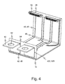
- Fig. 4 shows a three-dimensional representation of the second power semiconductor module according to the invention.
- Fig. 5 shows a variation of the second embodiment of the power semiconductor module according to the invention.
- Fig. 1 shows a step of the manufacturing method of a power semiconductor module according to the invention. Shown are a substrate (10) with an insulating body (12) and power semiconductor components (14) arranged thereon, as well as a load connection element (50).
- the load connection element (50) is here designed as a flat metal shaped body with a predetermined bending point (54) for the later formation of an angular configuration of the load connection element (50).
- connection device (40) has a layer sequence of a first electrically conductive structured metal foil (42), an electrically insulating foil (44) and a second electrically conductive structured metal foil (46).
- the respective structurings form first and second conductor tracks from the respective metal foils.
- the electrically conductive connections of respective third contact surfaces (200) of the power semiconductor component or second contact surfaces (500) of the load connection element (50) to associated first contact surfaces (420) of the first Conductor track (42) of the connecting device (40) are formed by means of a pressure sintered connection. Also shown is a bending area (48, see also Fig. 2 ) on which the connecting device is angled before arrangement with the housing.
- the insulating film (44) of the connecting device (40) projects beyond all first printed conductors (42) in the direction from the substrate (10) to the edge of the film (44), such that from first (42) to second printed conductors (46) Sufficient clearance is provided at or near this edge to maintain air and creepage distances for electrical safety.
- Fig. 2 shows a basic embodiment of the power semiconductor module according to the invention and produced according to the invention. Shown is an insulating substrate (10), as it is in principle known in various embodiments from the application in power semiconductor modules. This has on its the interior of the power semiconductor module facing surface a plurality of connecting tracks (14, see. Fig. 1 ) on. Power semiconductor components (20) are arranged on these connecting tracks (14) and are preferably connected to the connecting tracks by means of soldered or sintered connections.
- connection device 40, cf. Fig. 1
- connection device which in turn consists of a layer sequence with a first electrically conductive structured metal foil (42), an electrically insulating foil (44) and a second electrically conductive structured foil (46). If necessary, this layer sequence can be continued alternately.
- the respective structurings of the first and second metal foils form first and second interconnects each electrically insulated from one another.
- interconnects (42, 46) not only serve the internal circuit-compatible connection within the power semiconductor module (20) but also form parts of the external connection elements.
- the connecting device (40) has at least one region which is not arranged parallel to the substrate surface. This area is preferably perpendicular to the plane formed by the substrate surface and has on first conductor tracks (42) first contact surfaces (420) for connection to second contact surfaces (500) of load connection elements (50), of which only one is shown on.
- This load connection element (50) consists of an angular metal shaped part whose first leg with its outside which forms the contact surface (500) is arranged on the first contact surface (420) of the first conductor track (42) of the connection device (40) and whose second leg is a recess (52) for a screw leadthrough (56). This second leg is arranged parallel to the substrate (10).
- the first interconnect (42) associated with the load connection element (50) extends as far as the plane formed by the surface of the second leg of the load connection element (50) facing away from the substrate (10), small tolerances being harmless as long as the necessary airflow is achieved. and creepage distances (70) are complied with.
- the insulating film (44) of the connecting device (40) as well as the second conductor tracks (46) project beyond this plane, wherein the second conductor tracks (46) lead here no load potential, but control and / or sensor potentials.
- This extension beyond the said plane is designed such that the necessary air and creepage distances (70) are formed by the insulating film to ensure the electrical safety of the power semiconductor module between load and control potential.
- the housing (30) of the power semiconductor module is likewise shown schematically, this enclosing the substrate (10) completely and the load connection elements (50) in such a way that external contacting by means of a screw connection (56, 58) is permitted.
- the insulating film (44) and the second conductor tracks (46) project out of the housing (30) in order to form external auxiliary connection elements there.
- Fig. 3 shows a second embodiment of the invention of the power semiconductor module.
- the power semiconductor module is in turn formed from the two essential components, the housing (30) and the substrate (10) with power semiconductor components (20), connection device (40) and load connection elements (50).
- power semiconductor components (20), connection device (40) and load connection elements (50) For this purpose, in a first step of the production of these second component by way of example by means of the method step according to Fig. 1 educated. In general, this is preferably done by solder and / or pressure sintered connections.
- the connection device (40) is connected to the power semiconductor components (20) and in a next step the connection between the power semiconductor components (20) and the substrate (10) and at the same time the connection between the load connection elements (50) and the connection device (40).
- any sequential formation of all individual connections is also possible by means of different technologies.
- the load connection element (50) along the predetermined bending point (54, see FIG. Fig. 1 ) is brought into the angled shape and subsequently the component is joined to the housing (30).
- a part of the connecting device (40) namely a part of the insulating film (44) and second printed conductors (46), projects out of the housing (30).
- auxiliary contact pads (46) for a single or multi-pole plug contact which can be arranged in a connector (62) of an external circuit board (60).
- the flexibility of the connecting device (40) virtually automatically forms a traction interruption, whereby a secure plug connection is ensured.
- the connector (62) for connecting the control and / or sensor signals is advantageously arranged on the external circuit board with driver circuits, which in turn can be arranged at a distance from the housing (30) of the power semiconductor module and parallel to its substrate (10).
- Fig. 4 shows a three-dimensional representation of the second power semiconductor module according to the invention. Here is the course of the under Fig. 3 again clearly visible first and second printed conductors (42, 46).
- Fig. 5 shows a variation of the second embodiment of the power semiconductor module according to the invention. This differs to the effect that the auxiliary contact connection surfaces (460) of the second conductor tracks (46) comes to rest on the side facing away from the housing (30) from the protruding section of the connection device (40) by a 180 ° offset of the connection device (40).
- an electrical connection to an overlying external circuit board (60) is easily possible by pressure (64) is exerted on the connection to the second interconnects (46) via the circuit board (60).
- the housing (32) forms an abutment for this pressure introduction.
- the housing (30) is formed here only in the production of the power semiconductor module by at least the load connection element (50) is enclosed by means of a spraying process.
- the load connection element (50) is enclosed by means of a spraying process.
Landscapes
- Cooling Or The Like Of Semiconductors Or Solid State Devices (AREA)
- Inverter Devices (AREA)
- Combinations Of Printed Boards (AREA)
- Details Of Connecting Devices For Male And Female Coupling (AREA)
- Structures For Mounting Electric Components On Printed Circuit Boards (AREA)
Applications Claiming Priority (1)
| Application Number | Priority Date | Filing Date | Title |
|---|---|---|---|
| DE102009024385A DE102009024385B4 (de) | 2009-06-09 | 2009-06-09 | Verfahren zur Herstellung eines Leistungshalbleitermoduls und Leistungshalbleitermodul mit einer Verbindungseinrichtung |
Publications (2)
| Publication Number | Publication Date |
|---|---|
| EP2264761A2 true EP2264761A2 (fr) | 2010-12-22 |
| EP2264761A3 EP2264761A3 (fr) | 2016-07-13 |
Family
ID=42378054
Family Applications (1)
| Application Number | Title | Priority Date | Filing Date |
|---|---|---|---|
| EP10004376.9A Withdrawn EP2264761A3 (fr) | 2009-06-09 | 2010-04-24 | Procédé de fabrication d'un module semi-conducteur de puissance et module semi-conducteur de puissance doté d'un dispositif de raccordement |
Country Status (6)
| Country | Link |
|---|---|
| US (1) | US8283784B2 (fr) |
| EP (1) | EP2264761A3 (fr) |
| JP (1) | JP5520696B2 (fr) |
| KR (1) | KR101672548B1 (fr) |
| CN (1) | CN101924044B (fr) |
| DE (1) | DE102009024385B4 (fr) |
Families Citing this family (6)
| Publication number | Priority date | Publication date | Assignee | Title |
|---|---|---|---|---|
| JP5434857B2 (ja) * | 2010-09-15 | 2014-03-05 | 株式会社デンソー | 半導体モジュール |
| DE102010063387A1 (de) | 2010-12-17 | 2012-06-21 | Semikron Elektronik Gmbh & Co. Kg | Schaltungsanordnung mit mindestens zwei Teilmoduln |
| JP5842489B2 (ja) * | 2011-09-14 | 2016-01-13 | 三菱電機株式会社 | 半導体装置 |
| DE102013200526B4 (de) * | 2013-01-16 | 2019-11-21 | Semikron Elektronik Gmbh & Co. Kg | Leistungshalbleitermodul und Verfahren zur Herstellung eines Leistungshalbleitermoduls |
| JP6138181B2 (ja) | 2014-04-15 | 2017-05-31 | キヤノン株式会社 | 画像形成装置に用いられる樹脂成形品及びカートリッジ、並びに画像形成装置に用いられる可動部材の製造方法及びカートリッジの製造方法 |
| DE102016113152B4 (de) * | 2016-07-18 | 2019-12-19 | Semikron Elektronik Gmbh & Co. Kg | Leistungselektronische Schalteinrichtung und Leistungshalbleitermodul hiermit |
Citations (1)
| Publication number | Priority date | Publication date | Assignee | Title |
|---|---|---|---|---|
| DE102006027482B3 (de) | 2006-06-14 | 2007-08-16 | Semikron Elektronik Gmbh & Co. Kg | Gehauste Halbleiterschaltungsanordnung mit Kontakteinrichtung |
Family Cites Families (18)
| Publication number | Priority date | Publication date | Assignee | Title |
|---|---|---|---|---|
| JP2002093995A (ja) * | 2000-09-20 | 2002-03-29 | Unisia Jecs Corp | 半導体装置 |
| DE10237561C1 (de) * | 2002-08-16 | 2003-10-16 | Semikron Elektronik Gmbh | Induktivitätsarme Schaltungsanordnung bzw. Schaltungsaufbau für Leistungshalbleitermodule |
| DE10309302B4 (de) * | 2003-03-04 | 2007-09-27 | Semikron Elektronik Gmbh & Co. Kg | Leistungshalbleitermodul mit Sensorbauteil |
| JP3898156B2 (ja) * | 2003-06-02 | 2007-03-28 | 三菱電機株式会社 | 半導体パワーモジュール |
| JP4282417B2 (ja) * | 2003-09-12 | 2009-06-24 | ソニーケミカル&インフォメーションデバイス株式会社 | 接続構造体 |
| DE10355925B4 (de) * | 2003-11-29 | 2006-07-06 | Semikron Elektronik Gmbh & Co. Kg | Leistungshalbleitermodul und Verfahren seiner Herstellung |
| JP4265394B2 (ja) * | 2003-12-17 | 2009-05-20 | 株式会社日立製作所 | 電力変換装置 |
| DE102005024900B4 (de) * | 2004-06-08 | 2012-08-16 | Fuji Electric Co., Ltd. | Leistungsmodul |
| DE102005039278A1 (de) * | 2005-08-19 | 2007-02-22 | Semikron Elektronik Gmbh & Co. Kg | Leistungshalbleitermodul mit Leitungselement |
| WO2007025489A1 (fr) * | 2005-08-26 | 2007-03-08 | Siemens Aktiengesellschaft | Module semi-conducteur de puissance pourvu d'elements de connexion de charge places sur des supports de circuits |
| DE102005047567B3 (de) * | 2005-10-05 | 2007-03-29 | Semikron Elektronik Gmbh & Co. Kg | Leistungshalbleitermodul mit Isolationszwischenlage und Verfahren zu seiner Herstellung |
| DE102005049687B4 (de) * | 2005-10-14 | 2008-09-25 | Infineon Technologies Ag | Leistungshalbleiterbauteil in Flachleitertechnik mit vertikalem Strompfad und Verfahren zur Herstellung |
| DE102006013078B4 (de) * | 2006-03-22 | 2008-01-03 | Semikron Elektronik Gmbh & Co. Kg | Kompaktes Leistungshalbleitermodul mit Verbindungseinrichtung |
| US9373563B2 (en) * | 2007-07-20 | 2016-06-21 | Infineon Technologies Ag | Semiconductor assembly having a housing |
| JP5192194B2 (ja) * | 2007-07-26 | 2013-05-08 | デクセリアルズ株式会社 | 接着フィルム |
| DE102007054710B3 (de) * | 2007-11-16 | 2009-07-09 | Semikron Elektronik Gmbh & Co. Kg | Verfahren zur Herstellung einer Halbleiterbaugruppe |
| DE102008017454B4 (de) * | 2008-04-05 | 2010-02-04 | Semikron Elektronik Gmbh & Co. Kg | Leistungshalbleitermodul mit hermetisch dichter Schaltungsanordnung und Herstellungsverfahren hierzu |
| DE102009017733B4 (de) * | 2009-04-11 | 2011-12-08 | Semikron Elektronik Gmbh & Co. Kg | Leistungshalbleitermodul mit einer Verbindungseinrichtung und mit als Kontaktfeder ausgebildeten internen Anschlusselementen |
-
2009
- 2009-06-09 DE DE102009024385A patent/DE102009024385B4/de not_active Expired - Fee Related
-
2010
- 2010-04-24 EP EP10004376.9A patent/EP2264761A3/fr not_active Withdrawn
- 2010-06-01 JP JP2010125775A patent/JP5520696B2/ja active Active
- 2010-06-09 US US12/797,331 patent/US8283784B2/en not_active Expired - Fee Related
- 2010-06-09 KR KR1020100054373A patent/KR101672548B1/ko not_active Expired - Fee Related
- 2010-06-09 CN CN201010202629.6A patent/CN101924044B/zh active Active
Patent Citations (1)
| Publication number | Priority date | Publication date | Assignee | Title |
|---|---|---|---|---|
| DE102006027482B3 (de) | 2006-06-14 | 2007-08-16 | Semikron Elektronik Gmbh & Co. Kg | Gehauste Halbleiterschaltungsanordnung mit Kontakteinrichtung |
Also Published As
| Publication number | Publication date |
|---|---|
| KR20100132467A (ko) | 2010-12-17 |
| JP2010287887A (ja) | 2010-12-24 |
| DE102009024385A1 (de) | 2010-12-16 |
| CN101924044A (zh) | 2010-12-22 |
| KR101672548B1 (ko) | 2016-11-16 |
| EP2264761A3 (fr) | 2016-07-13 |
| US20110001244A1 (en) | 2011-01-06 |
| US8283784B2 (en) | 2012-10-09 |
| DE102009024385B4 (de) | 2011-03-17 |
| JP5520696B2 (ja) | 2014-06-11 |
| CN101924044B (zh) | 2014-07-30 |
Similar Documents
| Publication | Publication Date | Title |
|---|---|---|
| EP1956647B1 (fr) | Circuit doté d'un dispositif de liaison et son procédé de fabrication | |
| EP2107604B1 (fr) | Module semi-conducteur de puissance doté d'un circuit étanche hermétique et son procédé de fabrication | |
| EP1898466B1 (fr) | Circuit semi-conducteur dans un boîtier doté d'un dispositif de contact | |
| DE10306643B4 (de) | Anordnung in Druckkontaktierung mit einem Leistungshalbleitermodul | |
| EP2332247A1 (fr) | Ensemble condensateur et procédé de fabrication d'un ensemble condensateur | |
| DE102016002052A1 (de) | Schaltschrank sowie Verfahren zu dessen Herstellung | |
| DE102009024385B4 (de) | Verfahren zur Herstellung eines Leistungshalbleitermoduls und Leistungshalbleitermodul mit einer Verbindungseinrichtung | |
| EP2284889A1 (fr) | Module semi-conducteur de puissance doté d'un support de commutation et d'un élément de raccordement de charge ainsi que procédé de fabrication correspondant | |
| DE112016005794T5 (de) | Schaltungsanordnung und elektrischer Anschlusskasten | |
| WO2009030553A1 (fr) | Dispositif de commutation électrique comprenant un support de circuit mid et une interface de connexion associée | |
| EP2595249B1 (fr) | Borne de connexion | |
| EP2277242B1 (fr) | Mise en contact de réglettes de contacts à couteaux par le biais de cartes de circuit imprimé intermédiaires | |
| DE102008012256A1 (de) | Elektronik-Komponenten-Montageplatte | |
| EP1772902B1 (fr) | Module semiconducteur de puissance avec couche isolante intermédiaire et méthode de fabrication | |
| EP2819492A1 (fr) | Composant MID, procédé de fabrication | |
| WO2014187834A2 (fr) | Module électronique, en particulier appareil de commande pour un véhicule et procédé de production dudit module électronique | |
| DE102005055713A1 (de) | Leistungshalbleitermodul mit Anschlusselementen | |
| DE102016218970A1 (de) | Elektronikmodul und Verfahren zur Herstellung eines Elektronikmoduls | |
| DE102016115373B4 (de) | Schaltungsanordnung mit einer Verbindungseinrichtung und mit einer Leiterplatte | |
| DE102008052925A1 (de) | Schnittstelle von Sammelschiene mit gedruckter Leiterplatte für Elektro- und Hybridelektrofahrzeuge | |
| DE10328285A1 (de) | Leiterplatte | |
| DE102007037841A1 (de) | Trägermodul und Verfahren zur Herstellung eines Trägermoduls | |
| EP2099266B1 (fr) | Transducteur ultrasonore doté d'une plaquette flexible | |
| DE10209648A1 (de) | Kontaktierungseinheit zur elektrisch leitenden Verbindung zweier elektronischer Baugruppen | |
| EP2148367A1 (fr) | Module semi-conducteur de puissance |
Legal Events
| Date | Code | Title | Description |
|---|---|---|---|
| PUAI | Public reference made under article 153(3) epc to a published international application that has entered the european phase |
Free format text: ORIGINAL CODE: 0009012 |
|
| AK | Designated contracting states |
Kind code of ref document: A2 Designated state(s): AT BE BG CH CY CZ DE DK EE ES FI FR GB GR HR HU IE IS IT LI LT LU LV MC MK MT NL NO PL PT RO SE SI SK SM TR |
|
| AX | Request for extension of the european patent |
Extension state: AL BA ME RS |
|
| PUAL | Search report despatched |
Free format text: ORIGINAL CODE: 0009013 |
|
| AK | Designated contracting states |
Kind code of ref document: A3 Designated state(s): AT BE BG CH CY CZ DE DK EE ES FI FR GB GR HR HU IE IS IT LI LT LU LV MC MK MT NL NO PL PT RO SE SI SK SM TR |
|
| AX | Request for extension of the european patent |
Extension state: AL BA ME RS |
|
| RIC1 | Information provided on ipc code assigned before grant |
Ipc: H01L 23/538 20060101ALI20160608BHEP Ipc: H01L 23/049 20060101ALI20160608BHEP Ipc: H01L 23/00 20060101ALI20160608BHEP Ipc: H01L 23/48 20060101ALI20160608BHEP Ipc: H01L 25/07 20060101AFI20160608BHEP |
|
| 17P | Request for examination filed |
Effective date: 20170113 |
|
| STAA | Information on the status of an ep patent application or granted ep patent |
Free format text: STATUS: THE APPLICATION HAS BEEN WITHDRAWN |
|
| 17Q | First examination report despatched |
Effective date: 20170810 |
|
| 18W | Application withdrawn |
Effective date: 20170904 |