EP2264780A2 - Nanostrukturierte Solarzelle - Google Patents
Nanostrukturierte Solarzelle Download PDFInfo
- Publication number
- EP2264780A2 EP2264780A2 EP10165595A EP10165595A EP2264780A2 EP 2264780 A2 EP2264780 A2 EP 2264780A2 EP 10165595 A EP10165595 A EP 10165595A EP 10165595 A EP10165595 A EP 10165595A EP 2264780 A2 EP2264780 A2 EP 2264780A2
- Authority
- EP
- European Patent Office
- Prior art keywords
- electrode
- solar cell
- electron
- conducting
- nanostructure
- Prior art date
- Legal status (The legal status is an assumption and is not a legal conclusion. Google has not performed a legal analysis and makes no representation as to the accuracy of the status listed.)
- Withdrawn
Links
- 239000002086 nanomaterial Substances 0.000 claims abstract description 34
- 239000004020 conductor Substances 0.000 claims abstract description 26
- 239000006096 absorbing agent Substances 0.000 claims abstract description 15
- 239000011148 porous material Substances 0.000 claims description 9
- 239000002071 nanotube Substances 0.000 claims description 8
- 239000002070 nanowire Substances 0.000 claims description 8
- 238000000034 method Methods 0.000 claims description 7
- 239000011358 absorbing material Substances 0.000 claims description 6
- 239000000243 solution Substances 0.000 claims description 4
- 239000012530 fluid Substances 0.000 claims description 3
- 239000000758 substrate Substances 0.000 claims description 3
- 239000003792 electrolyte Substances 0.000 claims description 2
- 239000011245 gel electrolyte Substances 0.000 claims description 2
- 238000002347 injection Methods 0.000 claims description 2
- 239000007924 injection Substances 0.000 claims description 2
- 239000002608 ionic liquid Substances 0.000 claims description 2
- 239000000203 mixture Substances 0.000 claims description 2
- 229920000642 polymer Polymers 0.000 claims description 2
- QHGNHLZPVBIIPX-UHFFFAOYSA-N tin(ii) oxide Chemical class [Sn]=O QHGNHLZPVBIIPX-UHFFFAOYSA-N 0.000 claims description 2
- 230000002194 synthesizing effect Effects 0.000 claims 1
- 239000002096 quantum dot Substances 0.000 abstract description 3
- 239000000463 material Substances 0.000 description 7
- 230000006798 recombination Effects 0.000 description 5
- 238000005215 recombination Methods 0.000 description 5
- 239000004065 semiconductor Substances 0.000 description 5
- GWEVSGVZZGPLCZ-UHFFFAOYSA-N titanium dioxide Inorganic materials O=[Ti]=O GWEVSGVZZGPLCZ-UHFFFAOYSA-N 0.000 description 5
- XLOMVQKBTHCTTD-UHFFFAOYSA-N Zinc monoxide Chemical compound [Zn]=O XLOMVQKBTHCTTD-UHFFFAOYSA-N 0.000 description 4
- 238000000224 chemical solution deposition Methods 0.000 description 3
- 238000006243 chemical reaction Methods 0.000 description 2
- 238000005229 chemical vapour deposition Methods 0.000 description 2
- 238000000151 deposition Methods 0.000 description 2
- 230000008021 deposition Effects 0.000 description 2
- 238000004519 manufacturing process Methods 0.000 description 2
- 230000007246 mechanism Effects 0.000 description 2
- 239000002105 nanoparticle Substances 0.000 description 2
- 231100000252 nontoxic Toxicity 0.000 description 2
- 230000003000 nontoxic effect Effects 0.000 description 2
- BASFCYQUMIYNBI-UHFFFAOYSA-N platinum Chemical compound [Pt] BASFCYQUMIYNBI-UHFFFAOYSA-N 0.000 description 2
- 238000001179 sorption measurement Methods 0.000 description 2
- 239000011787 zinc oxide Substances 0.000 description 2
- GYHNNYVSQQEPJS-UHFFFAOYSA-N Gallium Chemical compound [Ga] GYHNNYVSQQEPJS-UHFFFAOYSA-N 0.000 description 1
- OAICVXFJPJFONN-UHFFFAOYSA-N Phosphorus Chemical compound [P] OAICVXFJPJFONN-UHFFFAOYSA-N 0.000 description 1
- XUIMIQQOPSSXEZ-UHFFFAOYSA-N Silicon Chemical compound [Si] XUIMIQQOPSSXEZ-UHFFFAOYSA-N 0.000 description 1
- RTAQQCXQSZGOHL-UHFFFAOYSA-N Titanium Chemical compound [Ti] RTAQQCXQSZGOHL-UHFFFAOYSA-N 0.000 description 1
- 238000002048 anodisation reaction Methods 0.000 description 1
- 238000003491 array Methods 0.000 description 1
- 230000015572 biosynthetic process Effects 0.000 description 1
- 229910052793 cadmium Inorganic materials 0.000 description 1
- -1 cadmium chalcogenide Chemical class 0.000 description 1
- 239000000969 carrier Substances 0.000 description 1
- 238000010586 diagram Methods 0.000 description 1
- 229910052733 gallium Inorganic materials 0.000 description 1
- 239000011521 glass Substances 0.000 description 1
- 238000001027 hydrothermal synthesis Methods 0.000 description 1
- 229910052738 indium Inorganic materials 0.000 description 1
- APFVFJFRJDLVQX-UHFFFAOYSA-N indium atom Chemical compound [In] APFVFJFRJDLVQX-UHFFFAOYSA-N 0.000 description 1
- AMGQUBHHOARCQH-UHFFFAOYSA-N indium;oxotin Chemical compound [In].[Sn]=O AMGQUBHHOARCQH-UHFFFAOYSA-N 0.000 description 1
- 239000002120 nanofilm Substances 0.000 description 1
- 230000003287 optical effect Effects 0.000 description 1
- 239000002245 particle Substances 0.000 description 1
- 230000035515 penetration Effects 0.000 description 1
- 229910052698 phosphorus Inorganic materials 0.000 description 1
- 239000011574 phosphorus Substances 0.000 description 1
- 229910052697 platinum Inorganic materials 0.000 description 1
- 238000001338 self-assembly Methods 0.000 description 1
- 229910052710 silicon Inorganic materials 0.000 description 1
- 239000010703 silicon Substances 0.000 description 1
- 239000002904 solvent Substances 0.000 description 1
- 238000003786 synthesis reaction Methods 0.000 description 1
- 229910052719 titanium Inorganic materials 0.000 description 1
- 239000010936 titanium Substances 0.000 description 1
- 239000004408 titanium dioxide Substances 0.000 description 1
- 239000003440 toxic substance Substances 0.000 description 1
Images
Classifications
-
- H—ELECTRICITY
- H10—SEMICONDUCTOR DEVICES; ELECTRIC SOLID-STATE DEVICES NOT OTHERWISE PROVIDED FOR
- H10F—INORGANIC SEMICONDUCTOR DEVICES SENSITIVE TO INFRARED RADIATION, LIGHT, ELECTROMAGNETIC RADIATION OF SHORTER WAVELENGTH OR CORPUSCULAR RADIATION
- H10F71/00—Manufacture or treatment of devices covered by this subclass
-
- B—PERFORMING OPERATIONS; TRANSPORTING
- B82—NANOTECHNOLOGY
- B82Y—SPECIFIC USES OR APPLICATIONS OF NANOSTRUCTURES; MEASUREMENT OR ANALYSIS OF NANOSTRUCTURES; MANUFACTURE OR TREATMENT OF NANOSTRUCTURES
- B82Y30/00—Nanotechnology for materials or surface science, e.g. nanocomposites
-
- H—ELECTRICITY
- H01—ELECTRIC ELEMENTS
- H01G—CAPACITORS; CAPACITORS, RECTIFIERS, DETECTORS, SWITCHING DEVICES, LIGHT-SENSITIVE OR TEMPERATURE-SENSITIVE DEVICES OF THE ELECTROLYTIC TYPE
- H01G9/00—Electrolytic capacitors, rectifiers, detectors, switching devices, light-sensitive or temperature-sensitive devices; Processes of their manufacture
- H01G9/20—Light-sensitive devices
- H01G9/2027—Light-sensitive devices comprising an oxide semiconductor electrode
- H01G9/2031—Light-sensitive devices comprising an oxide semiconductor electrode comprising titanium oxide, e.g. TiO2
-
- H—ELECTRICITY
- H10—SEMICONDUCTOR DEVICES; ELECTRIC SOLID-STATE DEVICES NOT OTHERWISE PROVIDED FOR
- H10F—INORGANIC SEMICONDUCTOR DEVICES SENSITIVE TO INFRARED RADIATION, LIGHT, ELECTROMAGNETIC RADIATION OF SHORTER WAVELENGTH OR CORPUSCULAR RADIATION
- H10F77/00—Constructional details of devices covered by this subclass
- H10F77/10—Semiconductor bodies
- H10F77/14—Shape of semiconductor bodies; Shapes, relative sizes or dispositions of semiconductor regions within semiconductor bodies
-
- H—ELECTRICITY
- H10—SEMICONDUCTOR DEVICES; ELECTRIC SOLID-STATE DEVICES NOT OTHERWISE PROVIDED FOR
- H10K—ORGANIC ELECTRIC SOLID-STATE DEVICES
- H10K30/00—Organic devices sensitive to infrared radiation, light, electromagnetic radiation of shorter wavelength or corpuscular radiation
- H10K30/10—Organic devices sensitive to infrared radiation, light, electromagnetic radiation of shorter wavelength or corpuscular radiation comprising heterojunctions between organic semiconductors and inorganic semiconductors
- H10K30/15—Sensitised wide-bandgap semiconductor devices, e.g. dye-sensitised TiO2
- H10K30/151—Sensitised wide-bandgap semiconductor devices, e.g. dye-sensitised TiO2 the wide bandgap semiconductor comprising titanium oxide, e.g. TiO2
-
- H—ELECTRICITY
- H01—ELECTRIC ELEMENTS
- H01G—CAPACITORS; CAPACITORS, RECTIFIERS, DETECTORS, SWITCHING DEVICES, LIGHT-SENSITIVE OR TEMPERATURE-SENSITIVE DEVICES OF THE ELECTROLYTIC TYPE
- H01G9/00—Electrolytic capacitors, rectifiers, detectors, switching devices, light-sensitive or temperature-sensitive devices; Processes of their manufacture
- H01G9/20—Light-sensitive devices
- H01G9/2054—Light-sensitive devices comprising a semiconductor electrode comprising AII-BVI compounds, e.g. CdTe, CdSe, ZnTe, ZnSe, with or without impurities, e.g. doping materials
-
- Y—GENERAL TAGGING OF NEW TECHNOLOGICAL DEVELOPMENTS; GENERAL TAGGING OF CROSS-SECTIONAL TECHNOLOGIES SPANNING OVER SEVERAL SECTIONS OF THE IPC; TECHNICAL SUBJECTS COVERED BY FORMER USPC CROSS-REFERENCE ART COLLECTIONS [XRACs] AND DIGESTS
- Y02—TECHNOLOGIES OR APPLICATIONS FOR MITIGATION OR ADAPTATION AGAINST CLIMATE CHANGE
- Y02E—REDUCTION OF GREENHOUSE GAS [GHG] EMISSIONS, RELATED TO ENERGY GENERATION, TRANSMISSION OR DISTRIBUTION
- Y02E10/00—Energy generation through renewable energy sources
- Y02E10/50—Photovoltaic [PV] energy
- Y02E10/542—Dye sensitized solar cells
-
- Y—GENERAL TAGGING OF NEW TECHNOLOGICAL DEVELOPMENTS; GENERAL TAGGING OF CROSS-SECTIONAL TECHNOLOGIES SPANNING OVER SEVERAL SECTIONS OF THE IPC; TECHNICAL SUBJECTS COVERED BY FORMER USPC CROSS-REFERENCE ART COLLECTIONS [XRACs] AND DIGESTS
- Y02—TECHNOLOGIES OR APPLICATIONS FOR MITIGATION OR ADAPTATION AGAINST CLIMATE CHANGE
- Y02E—REDUCTION OF GREENHOUSE GAS [GHG] EMISSIONS, RELATED TO ENERGY GENERATION, TRANSMISSION OR DISTRIBUTION
- Y02E10/00—Energy generation through renewable energy sources
- Y02E10/50—Photovoltaic [PV] energy
- Y02E10/549—Organic PV cells
Definitions
- Transparent porous films such as Ti02 nanoparticle (NP) films have played an important role as electron conductors in devices like dye sensitized solar calls.
- electrons injected from the light absorbing sensitizer are subject to losses from the many particle boundaries along random, tortuous, transport paths.
- Other solar cell devices utilizing nanostructures also suffer from inefficiencies in the electron transport paths. Recombination losses at the absorber - electron conductor and hole conductor interfaces - will limit the overall utility of prior nano-enabled solar cells.
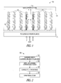
- FIG. 1 is a cross sectional block representation of a nano-structured solar cell 100.
- the solar cell 100 has a first electrode 110.
- An array of electrically conductive nanostructure films 115 are electrically coupled to and supported by the first electrode 110.
- the nanostructure films 115 comprise nanowires, nanotubes, or a combination of both. The films may be ordered such as by rows and columns, or somewhat random with an average spacing in various embodiments.
- a plurality of nanocrystalline absorbers 120 are attached to the electron conductive nanostructure films 115. Examples of nanocrystalline light absorbers include, but are not limited to, semiconductor quantum dots, thin continuous semiconductor films, and thin discontinuous semiconductor films.
- a hole conducting material 125 is disposed or diffused between the electron conducting nanostructure films 115.
- the nanostructure films 115 provide a highly textured surface in one embodiment, such that the surface are of the films is greatly increased.
- the hole conducting material 125 thus infiltrates between and into the textured surface of the films.
- a second electrode 130 is electrically coupled to the hole conducting material 125.
- the first electrode 110 may be transparent, and comprises an anode and the second electrode 130 comprises a cathode.
- the first electrode 110 may be formed utilizing a fluorinated tin oxide or indium tin oxide coated flexible substrate.
- the substrate may be formed of glass with a conductive top layer that is electrically coupled to the nanostructured film 115.
- the second electrode is formed of platinum with some titanium.
- the second electrode may be reflective in one embodiment, such that light entering the through the first electrode 110 may be absorbed by the nanocrystalline absorbers 120 to create electron hole pairs, and light not so absorbed, is reflected back through the film 115, some of which is also absorbed by the nanocrystalline absorbers 120 to create further electron hole pairs.
- the film 115 comprises an ordered array of nanowires and/or nanotubes that have a partially uniform nano-pore structure that allows better penetration for the hole conducting medium and growth path or attachment path for the nanocrystalline light absorbing material.
- the nanowires or nanotubes may be formed on the first electrode 110 in a self assembled manner utilizing a solution growth or anodization process.
- the film 115 may be formed using visibly transparent large band-gap semiconductors, such as TiO 2 or ZnO in various embodiments.
- the film 115 provides a high surface area porous electron conducting surface. In one embodiment, the film has a thickness of approximately 0.5 to 10 ⁇ m.
- the nanocrystalline light absorber may then be grown or formed directly on the film 115 via a chemical bath deposition (CBD), selective ionic layer adsorption and reaction (SILAR), chemical vapor deposition process, or by self assembly.
- CBD chemical bath deposition
- SILAR selective ionic layer adsorption and reaction
- chemical vapor deposition process or by self assembly.
- the hole conducting material 125 comprises a porous material having open pores, and a hole conductive fluid.
- the hole conductive fluid comprises at least one of an aqueous electrolyte, ionic liquid, gel electrolytes, and polymers in various embodiments.
- the porous material is part of the array of ordered electrically conductive nanostructure films and may provide support for at least one of nanowires and nanotubes.
- the hole conducting material 125 and second electrode 130 provide a hole conducting path.
- Such a nanowire or nanotube film 115 provides ordered nanostructures that serve as electron conductors.
- the nanostructures have a more continuous and straight crystalline structure, providing a straightforward path for electron transport.
- Such nanostructures may also provide pore structures that are inverted with respect to flat films. Such pore structures may be easier for hole conducting material to infiltrate, thus providing a similarly efficient transport path for holes and application of hole conducting material.
- a method of making the nano-structured solar cell 100 is illustrated generally at 200 in FIG. 2 .
- an ordered conductive nanostructure array is synthesized on a transparent conducting electrode.
- light absorbing nanocrystalline structures such as quantum dots, are grown onto the ordered conductive nanostructure array.
- Step 220 may also include attaching pre-grown light absorbing material to the nanostructured electron conductors synthesized at step 210.
- Step 220 may also include deposition of additional thin layers with the function of protecting the light absorber or electron conductor.
- Step 220 may also include the deposition of additional thin layers with the function of increasing the device performance by limiting recombination or increasing the ability for materials to bond with the electron conductor synthesized at step 210.
- a hole conducting material is added at 230 such that the hole conducting material infiltrates the nanostructure array.
- a reflective conducting electrode is provided that is electrically coupled to the hole conducting material.
- the nanostructure array may be synthesized by use of a chemical vapor deposition or hydrothermal process and may be formed of zinc oxide or titanium dioxide.
- the light absorbing nanostructures may be grown directly onto the ordered or somewhat random electron conducting nanostructure arrays using a solution based process, such as a chemical bath deposition or successive ionic layer adsorption reaction (SILAR).
- SILAR successive ionic layer adsorption reaction
- the absorbing material composition and geometry may be adjusted to control alignment of energy bands to ensure efficient electron injection.
- confining electronic carriers to nanometer sized dimensions in semiconductors alters the material's optical and electronic properties.
- the band-gap, valence band and conduction band energies can be tuned by changing the material's dimension. Tuning these energies can increase the performance and utility of a solar cell device.
- a material's dimension and geometry can be changed by altering one of the many growth parameters during the light absorber's synthesis. Examples of parameters that control the dimension and geometry of the nanocrystalline light absorber include growth time, pH, coordinating and non-coordinating solvent, relative concentration of the growth materials, and growth temperature. Different growth mechanisms for the nanocrystalline light absorbers - such as solution, vapor, and plasma - may have different mechanisms for changing the material's dimension and geometry.
- the light absorbing material comprises at least one of lead and cadmium chalcogenide, and ZnS.
- the light absorbing material comprises a non-toxic substance.
- non-toxic nanocrystalline absorbers include silicon and indium, gallium, phosphorus compisitions. These materials may be used to effectively span the visible light region. Adding layers of ZnS to the exposed surface of the nanostructures may help prevent trap states, increasing solar cell device efficiency by reducing recombination.
Landscapes
- Engineering & Computer Science (AREA)
- Chemical & Material Sciences (AREA)
- Nanotechnology (AREA)
- Power Engineering (AREA)
- Physics & Mathematics (AREA)
- Composite Materials (AREA)
- Materials Engineering (AREA)
- Crystallography & Structural Chemistry (AREA)
- General Physics & Mathematics (AREA)
- Condensed Matter Physics & Semiconductors (AREA)
- Microelectronics & Electronic Packaging (AREA)
- Inorganic Chemistry (AREA)
- Electromagnetism (AREA)
- Photovoltaic Devices (AREA)
- Hybrid Cells (AREA)
Applications Claiming Priority (1)
| Application Number | Priority Date | Filing Date | Title |
|---|---|---|---|
| US12/484,608 US20100313953A1 (en) | 2009-06-15 | 2009-06-15 | Nano-structured solar cell |
Publications (2)
| Publication Number | Publication Date |
|---|---|
| EP2264780A2 true EP2264780A2 (de) | 2010-12-22 |
| EP2264780A3 EP2264780A3 (de) | 2012-09-12 |
Family
ID=42767979
Family Applications (1)
| Application Number | Title | Priority Date | Filing Date |
|---|---|---|---|
| EP10165595A Withdrawn EP2264780A3 (de) | 2009-06-15 | 2010-06-10 | Nanostrukturierte Solarzelle |
Country Status (3)
| Country | Link |
|---|---|
| US (1) | US20100313953A1 (de) |
| EP (1) | EP2264780A3 (de) |
| CN (1) | CN101924151A (de) |
Cited By (1)
| Publication number | Priority date | Publication date | Assignee | Title |
|---|---|---|---|---|
| WO2016047615A1 (ja) * | 2014-09-24 | 2016-03-31 | 京セラ株式会社 | 光電変換装置および光電変換モジュール |
Families Citing this family (14)
| Publication number | Priority date | Publication date | Assignee | Title |
|---|---|---|---|---|
| KR101636907B1 (ko) * | 2009-12-08 | 2016-07-07 | 삼성전자주식회사 | 다공성 나노 구조체 및 그 제조 방법 |
| US20110277822A1 (en) * | 2010-05-11 | 2011-11-17 | Honeywell International Inc. | Composite electron conductor for use in photovoltaic devices |
| CN102683440A (zh) * | 2011-01-13 | 2012-09-19 | 霍尼韦尔国际公司 | 毫微结构的太阳能电池 |
| US20130298978A1 (en) * | 2011-01-31 | 2013-11-14 | Honeywell International Inc. | Quantum dot solar cell |
| CA2864212A1 (en) * | 2011-02-10 | 2012-08-16 | The Royal Institution For The Advancement Of Learning/Mcgill University | High efficiency broadband semiconductor nanowire devices and methods of fabricating without foreign metal catalysis |
| FR2972852B1 (fr) * | 2011-03-17 | 2013-04-12 | Commissariat Energie Atomique | Dispositif a base de nano/microfils stabilise mecaniquement et aux proprietes optiques ameliorees et son procede de realisation |
| WO2012155293A1 (en) * | 2011-05-17 | 2012-11-22 | Honeywell International Inc. | Novel electroconductive films for quantum dot sensitized solar cells |
| US8796693B2 (en) | 2012-12-26 | 2014-08-05 | Seoul Semiconductor Co., Ltd. | Successive ionic layer adsorption and reaction process for depositing epitaxial ZnO on III-nitride-based light emitting diode and light emitting diode including epitaxial ZnO |
| KR101410668B1 (ko) | 2013-06-04 | 2014-06-25 | 포항공과대학교 산학협력단 | 친환경 양자점 감응형 태양전지 및 이의 제조방법 |
| CN104944404B (zh) * | 2014-03-26 | 2019-05-31 | 清华大学 | 纳米管膜 |
| CN106057956A (zh) * | 2016-06-27 | 2016-10-26 | 浙江大学 | 一种基于离子液体凝胶电解质的准固态柔性自供能型ZnO基紫外探测器及其制备方法 |
| CN110311021B (zh) * | 2019-06-27 | 2020-11-10 | 深圳市华星光电半导体显示技术有限公司 | 量子点发光二极管器件及其制备方法 |
| EP4084104A4 (de) * | 2019-12-24 | 2023-06-07 | Panasonic Intellectual Property Management Co., Ltd. | Solarzelle |
| CN112909108A (zh) * | 2021-01-15 | 2021-06-04 | 重庆科技学院 | 基于量子点的壳芯结构纳米线阵列太阳能电池 |
Family Cites Families (7)
| Publication number | Priority date | Publication date | Assignee | Title |
|---|---|---|---|---|
| KR20070044981A (ko) * | 2005-10-26 | 2007-05-02 | 삼성전자주식회사 | 태양전지 구동형 표시소자 및 그의 제조방법 |
| KR20070056581A (ko) * | 2005-11-30 | 2007-06-04 | 삼성전자주식회사 | 태양전지용 전극, 그의 제조방법 및 그를 포함하는태양전지 |
| CN101411001A (zh) * | 2006-02-16 | 2009-04-15 | 索莱赞特公司 | 纳米颗粒敏化的纳米结构的太阳能电池 |
| TW200802903A (en) * | 2006-02-16 | 2008-01-01 | Solexant Corp | Nanoparticle sensitized nanostructured solar cells |
| US20070295388A1 (en) * | 2006-05-05 | 2007-12-27 | Nanosolar, Inc. | Solar assembly with a multi-ply barrier layer and individually encapsulated solar cells or solar cell strings |
| US20100043874A1 (en) * | 2007-06-26 | 2010-02-25 | Honeywell International Inc. | Nanostructured solar cell |
| US7910015B2 (en) * | 2007-10-22 | 2011-03-22 | Institute Of Nuclear Energy Research | Polymer electrolyte for dye sensitized solar cell |
-
2009
- 2009-06-15 US US12/484,608 patent/US20100313953A1/en not_active Abandoned
-
2010
- 2010-06-10 EP EP10165595A patent/EP2264780A3/de not_active Withdrawn
- 2010-06-13 CN CN2010102418822A patent/CN101924151A/zh active Pending
Non-Patent Citations (1)
| Title |
|---|
| None |
Cited By (2)
| Publication number | Priority date | Publication date | Assignee | Title |
|---|---|---|---|---|
| WO2016047615A1 (ja) * | 2014-09-24 | 2016-03-31 | 京セラ株式会社 | 光電変換装置および光電変換モジュール |
| JPWO2016047615A1 (ja) * | 2014-09-24 | 2017-05-18 | 京セラ株式会社 | 光電変換装置および光電変換モジュール |
Also Published As
| Publication number | Publication date |
|---|---|
| US20100313953A1 (en) | 2010-12-16 |
| EP2264780A3 (de) | 2012-09-12 |
| CN101924151A (zh) | 2010-12-22 |
Similar Documents
| Publication | Publication Date | Title |
|---|---|---|
| EP2264780A2 (de) | Nanostrukturierte Solarzelle | |
| Raj et al. | Improved photovoltaic performance of CdSe/CdS/PbS quantum dot sensitized ZnO nanorod array solar cell | |
| KR101131218B1 (ko) | 산화아연 나노 구조체 전극 제조 방법 및 이를 이용한 염료 감응형 태양 전지 제조 방법 | |
| JP4880597B2 (ja) | 針状結晶の配列体を含む複合体およびその製造方法、ならびに光電変換素子、発光素子およびキャパシタ | |
| KR101156531B1 (ko) | 플렉서블 반도체 전극의 제조방법 및 그에 의해 제조된반도체 전극, 이를 이용한 태양전지 | |
| JP2009507397A (ja) | ナノ構造およびそれを実施する光起電力セル | |
| US9452929B2 (en) | Photoelectrode including zinc oxide hemisphere, method of fabricating the same and dye-sensitized solar cell using the same | |
| KR101208272B1 (ko) | 양면 구조를 가지는 태양전지 및 이의 제조방법 | |
| US20150083605A1 (en) | Semiconductor photoelectrode and method for splitting water photoelectrochemically using photoelectrochemical cell comprising the same | |
| KR20130084218A (ko) | 나노구조체 및 이를 구현하는 광전지 | |
| JP2010533985A (ja) | 半導体の規則配列構造 | |
| Yin et al. | Strategies to prepare an efficient photoanode for ZnO nanowires-based CdS–CdSe co-sensitized solar cells | |
| Mahadik et al. | Highly efficient and stable 3D Ni (OH) 2/CdS/ZnIn2S4/TiO2 heterojunction under solar light: effect of an improved TiO2/FTO interface and cocatalyst | |
| JP2004343071A (ja) | 電子機器に用いられる多孔質膜、その多孔質膜の使用方法、電子機器、及びその多孔質膜の製造方法 | |
| US20130237006A1 (en) | Dye-sensitized solar cell and method of fabricating the same | |
| KR20120011871A (ko) | 나노스케일 아키텍쳐를 가지는 3차원 염료 감응 태양 전지 | |
| KR20160006187A (ko) | 고내구성, 고변환 효율을 갖는 색소 증감형 태양 전지 | |
| Wang et al. | Temperature-dependence photoelectrochemical hydrogen generation based on alloyed quantum dots | |
| CN103715280B (zh) | 一种微米/纳米二级阵列结构薄膜太阳能电池及其制备方法 | |
| KR101453605B1 (ko) | 양끝이 열린 산화티타늄 나노튜브 제조 및 이를 이용한 염료감응형 태양전지 | |
| KR20070078530A (ko) | 태양전지용 전극, 그의 제조방법 및 그를 포함하는태양전지 | |
| CN104851942B (zh) | ZnO/I掺杂ZnO核/壳结构纳米线阵列的制备方法 | |
| JP2005310821A (ja) | 光電変換素子 | |
| WO2013106793A1 (en) | Solar fuel generators | |
| Almamari et al. | Photoelectrochemical activity of magnetron sputtered ZnO thin films: role of thermal annealing |
Legal Events
| Date | Code | Title | Description |
|---|---|---|---|
| PUAI | Public reference made under article 153(3) epc to a published international application that has entered the european phase |
Free format text: ORIGINAL CODE: 0009012 |
|
| 17P | Request for examination filed |
Effective date: 20100610 |
|
| AK | Designated contracting states |
Kind code of ref document: A2 Designated state(s): AL AT BE BG CH CY CZ DE DK EE ES FI FR GB GR HR HU IE IS IT LI LT LU LV MC MK MT NL NO PL PT RO SE SI SK SM TR |
|
| AX | Request for extension of the european patent |
Extension state: BA ME RS |
|
| PUAL | Search report despatched |
Free format text: ORIGINAL CODE: 0009013 |
|
| AK | Designated contracting states |
Kind code of ref document: A3 Designated state(s): AL AT BE BG CH CY CZ DE DK EE ES FI FR GB GR HR HU IE IS IT LI LT LU LV MC MK MT NL NO PL PT RO SE SI SK SM TR |
|
| AX | Request for extension of the european patent |
Extension state: BA ME RS |
|
| RIC1 | Information provided on ipc code assigned before grant |
Ipc: H01L 31/18 20060101ALI20120808BHEP Ipc: H01L 31/0352 20060101AFI20120808BHEP Ipc: H01L 51/42 20060101ALI20120808BHEP Ipc: H01G 9/20 20060101ALI20120808BHEP |
|
| 17Q | First examination report despatched |
Effective date: 20120927 |
|
| RAP1 | Party data changed (applicant data changed or rights of an application transferred) |
Owner name: HONEYWELL INTERNATIONAL INC. |
|
| STAA | Information on the status of an ep patent application or granted ep patent |
Free format text: STATUS: THE APPLICATION IS DEEMED TO BE WITHDRAWN |
|
| 18D | Application deemed to be withdrawn |
Effective date: 20160105 |