EP2264792A2 - Dispositif électroluminescent et procédé de fabrication correspondant - Google Patents
Dispositif électroluminescent et procédé de fabrication correspondant Download PDFInfo
- Publication number
- EP2264792A2 EP2264792A2 EP09754966A EP09754966A EP2264792A2 EP 2264792 A2 EP2264792 A2 EP 2264792A2 EP 09754966 A EP09754966 A EP 09754966A EP 09754966 A EP09754966 A EP 09754966A EP 2264792 A2 EP2264792 A2 EP 2264792A2
- Authority
- EP
- European Patent Office
- Prior art keywords
- layer
- conductive semiconductor
- oxide
- semiconductor layer
- light emitting
- Prior art date
- Legal status (The legal status is an assumption and is not a legal conclusion. Google has not performed a legal analysis and makes no representation as to the accuracy of the status listed.)
- Granted
Links
Images


Classifications
-
- H—ELECTRICITY
- H10—SEMICONDUCTOR DEVICES; ELECTRIC SOLID-STATE DEVICES NOT OTHERWISE PROVIDED FOR
- H10H—INORGANIC LIGHT-EMITTING SEMICONDUCTOR DEVICES HAVING POTENTIAL BARRIERS
- H10H20/00—Individual inorganic light-emitting semiconductor devices having potential barriers, e.g. light-emitting diodes [LED]
- H10H20/80—Constructional details
- H10H20/84—Coatings, e.g. passivation layers or antireflective coatings
-
- H—ELECTRICITY
- H10—SEMICONDUCTOR DEVICES; ELECTRIC SOLID-STATE DEVICES NOT OTHERWISE PROVIDED FOR
- H10H—INORGANIC LIGHT-EMITTING SEMICONDUCTOR DEVICES HAVING POTENTIAL BARRIERS
- H10H20/00—Individual inorganic light-emitting semiconductor devices having potential barriers, e.g. light-emitting diodes [LED]
- H10H20/80—Constructional details
- H10H20/83—Electrodes
- H10H20/831—Electrodes characterised by their shape
- H10H20/8316—Multi-layer electrodes comprising at least one discontinuous layer
-
- H—ELECTRICITY
- H10—SEMICONDUCTOR DEVICES; ELECTRIC SOLID-STATE DEVICES NOT OTHERWISE PROVIDED FOR
- H10H—INORGANIC LIGHT-EMITTING SEMICONDUCTOR DEVICES HAVING POTENTIAL BARRIERS
- H10H20/00—Individual inorganic light-emitting semiconductor devices having potential barriers, e.g. light-emitting diodes [LED]
- H10H20/80—Constructional details
- H10H20/83—Electrodes
- H10H20/832—Electrodes characterised by their material
-
- H—ELECTRICITY
- H10—SEMICONDUCTOR DEVICES; ELECTRIC SOLID-STATE DEVICES NOT OTHERWISE PROVIDED FOR
- H10H—INORGANIC LIGHT-EMITTING SEMICONDUCTOR DEVICES HAVING POTENTIAL BARRIERS
- H10H20/00—Individual inorganic light-emitting semiconductor devices having potential barriers, e.g. light-emitting diodes [LED]
- H10H20/80—Constructional details
- H10H20/84—Coatings, e.g. passivation layers or antireflective coatings
- H10H20/841—Reflective coatings, e.g. dielectric Bragg reflectors
-
- H—ELECTRICITY
- H10—SEMICONDUCTOR DEVICES; ELECTRIC SOLID-STATE DEVICES NOT OTHERWISE PROVIDED FOR
- H10H—INORGANIC LIGHT-EMITTING SEMICONDUCTOR DEVICES HAVING POTENTIAL BARRIERS
- H10H20/00—Individual inorganic light-emitting semiconductor devices having potential barriers, e.g. light-emitting diodes [LED]
- H10H20/80—Constructional details
- H10H20/882—Scattering means
Definitions
- the embodiment relates to a light emitting device, and a method of manufacturing the same.
- a light emitting diode (LED) is spotlighted as a light emitting device. Since the LED can convert electric energy into light energy with high efficiency and long life span of about 5 years or more, the LED can remarkably reduce the energy consumption and repair and maintenance cost. In this regard, the LED is spotlighted in the next-generation lighting field.
- Such an LED is prepared as a light emitting semiconductor layer including a first conductive semiconductor layer, an active layer and a second conductive semiconductor layer, in which the active layer generates light according to current applied thereto through the first and second conductive semiconductor layers.
- a material constituting the light emitting semiconductor layer has a refractive index lower than that of external air, light generated from the active layer is not effectively emitted to the outside, but totally reflected from a boundary surface and extinguished at an inside of the light emitting semiconductor layer.
- a concave-convex light extracting structure is formed on the first conductive semiconductor layer or the second conductive semiconductor layer provided at one side of the active layer.
- the electrical characteristics of the LED may be degraded due to the light extracting structure.
- the embodiment provides a light emitting device having a novel structure and a method of manufacturing the same.
- the embodiment provides a light emitting device capable of improving the electrical characteristic and light extraction efficiency and a method of manufacturing the same.
- a light emitting device may include a first conductive semiconductor layer; an active layer on the first conductive semiconductor layer; a second conductive semiconductor layer on the active layer; a first passivation layer surrounding the first conductive semiconductor layer, the active layer, and the second conductive semiconductor layer; a second connection layer electrically connected to the second conductive semiconductor layer through the first passivation layer; a first light extracting structure layer on the first passivation layer and the second connection layer; a first electrode layer electrically connected to the first conductive semiconductor layer; and a second electrode layer on the first light extracting structure layer.
- a method of manufacturing a light emitting device may include the steps of forming a first conductive semiconductor layer on a growth substrate, an active layer on the first conductive semiconductor layer, and a second conductive semiconductor layer on the active layer; selectively removing the second conductive semiconductor layer, the active layer, and the first conductive semiconductor layer such that the first conductive semiconductor layer is partially exposed; forming a first passivation layer surrounding the first conductive semiconductor layer, the active layer, and the second conductive semiconductor layer; selectively removing the first passivation layer and forming a second connection layer electrically connected to the second conductive semiconductor layer; forming a first light extracting structure layer having a concave-convex structure on the second connection layer and the first passivation layer; and forming a second electrode layer on the first light extracting structure layer and forming a first electrode layer electrically connected to the first conductive semiconductor layer.
- the embodiment can provide a light emitting device having a novel structure and a method of manufacturing the same.
- the embodiment can provide a light emitting device capable of improving the electrical characteristic and light extraction efficiency and a method of manufacturing the same.
- each layer shown in the drawings may be exaggerated, omitted or schematically drawn for the purpose of convenience or clarity.
- the size of elements does not utterly reflect an actual size.
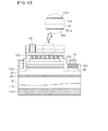
- FIG. 1 is a sectional view showing a light emitting device according to the first embodiment.
- a buffer layer 201 is formed on a growth substrate 10, and a light emitting semiconductor layer including a first conductive semiconductor layer 20, an active layer 30, and a second conductive semiconductor layer 40 is formed on the buffer layer 201.
- the light emitting semiconductor layer is partially removed through MESA etching, and a first current spreading layer 401 is formed on the first conductive semiconductor layer 20 exposed through the MESA etching.
- a second current spreading layer 501 is formed on a second conductive semiconductor layer 40.
- a first passivation layer 502 is formed to surround the light emitting semiconductor layer and the first and second current spreading layers 401 and 501.
- the first passivation layer 502 formed on the first and second current spreading layers 401 and 501 is selectively removed so that a via hole is formed.
- a first connection layer 403 and a second connection layer 503 are formed in the via hole.
- a first light extracting structure layer 504 is formed on the first passivation layer 502 and the second connection layer 503 formed on the second conductive semiconductor layer 40.
- a first electrode layer 70 is formed on the first connection layer 403 and a second electrode layer 60 is formed on the first light extracting structure layer 504.
- a second light extracting structure layer 110 is formed under the growth substrate 10 and a reflective layer 120 is formed under the second light extracting structure layer 110.
- the growth substrate 10 may include one of Al 2 O 3 , SiC, Si, AlN, GaN, AlGaN, glass and GaAs.
- the buffer layer 201 is formed on the growth substrate 10.
- the buffer layer 201 may include at least one of InGaN, AlN, SiC, SiCN, and GaN.
- the light emitting semiconductor layer including the first conductive semiconductor layer 20, the active layer 30, and the second conductive semiconductor layer 40 may include group-III nitride-based semiconductor materials.
- the first conductive semiconductor layer 20 may include a gallium nitride layer including n type impurities such as Si
- the second conductive semiconductor layer 40 may include a gallium nitride layer including p type impurities such as Mg.
- the active layer 30, which generates light through the recombination of electrons and holes may include one of InGaN, AlGaN, GaN, and AlInGaN. The wavelength of light emitted from the light emitting device is determined according to the type of materials constituting the active layer 30.
- the active layer 30 and the second conductive semiconductor layer 40 are formed on a part of the first conductive semiconductor layer 20.
- one part of the first conductive semiconductor layer 20 makes contact with the active layer 30 and the remaining part of the first conductive semiconductor layer 20 is exposed to the outside.
- an interface modification layer may be further formed on the second conductive semiconductor layer 40.
- the interface modification layer may include a superlattice structure, one of InGaN, GaN, AlInN, AlN, InN, and AlGaN doped with first conductive impurities, one of InGaN, GaN, AlInN, AlN, InN, and AlGaN doped with second conductive impurities, or one of group III nitride-based elements having nitrogen-polar surfaces.
- the interface modification layer having the superlattice structure may include nitride or carbon nitride including group II, III, or IV elements.
- the first current spreading layer 401 is partially formed on the first conductive semiconductor layer 20, and the second current spreading layer 501 is partially or wholly formed on the second conductive semiconductor layer 40.
- Both of the first and second current spreading layers 401 and 501 may not be necessarily required. That is, at least one of the first and second current spreading layers 401 and 501 may be omitted.
- the first and second current spreading layers 401 and 501 can be prepared as a single layer structure or a multi-layer structure including at least one selected from the group consisting of ITO (indium tin oxide), doped ZnO (doped Zinc oxide), TiN (titanium nitride), IZO (indium zinc oxide), IZTO (indium zinc tin oxide), NiO (nickel oxide), RuO 2 (ruthenium oxide), IrO 2 (iridium oxide), doped In 2 O 3 (doped indium oxide), Au, Ag, doped SnO 2 (doped tin oxide), GITO (gallium indium tin oxide), PdO (palladium oxide), PtO (platinum oxide), Ag 2 O (silver oxide), and doped TiO 2 (doped titanium oxide).
- ITO indium tin oxide
- doped ZnO doped Zinc oxide
- TiN titanium nitride
- IZO indium zinc oxide
- the first and second current spreading layers 401 and 501 uniformly spread current applied to the first and second conductive semiconductor layers 20 and 40, thereby improving light emitting efficiency.
- the first and second current spreading layers 401 and 501 allow the first and second electrode layers 70 and 60 to be sufficiently bonded to the first and second conductive semiconductor layers 20 and 40, respectively.
- the first passivation layer 502 is formed on the light emitting semiconductor layer including the first and second current spreading layers 401 and 501 except for some portions of the first and second current spreading layers 401 and 501.
- the first passivation layer 502 prevents the light emitting device from being physically, chemically, or electrically damaged.
- the first passivation layer 502 includes a transparent electric insulating material.
- the first passivation layer 502 includes at least one of SiO 2 (silicon dioxide), SiN x (silicon nitride), MgF 2 (magnesium fluoride), Cr 2 O 3 (chromium oxide), Al 2 O 3 (aluminum oxide), TiO 2 , ZnS (zinc sulfide), ZnO (zinc oxide), CaF 2 (calcium fluoride), AlN (aluminum nitride), and CrN (chromium nitride).
- the first and second connection layers 403 and 405 are formed on the first and second current spreading layers 401 and 501, respectively, while passing through the first passivation layer 502.
- the first passivation layer 502 formed on the first and second current spreading layers 401 and 501 has via holes and the via holes are filled with conductive materials to form the first and second connection layers 403 and 405.
- a plurality of via holes are formed in the first passivation layer 502 formed on the second current spreading layer 501, but the embodiment is not limited thereto. For instance, only one via hole can be formed in the first passivation layer 502 formed on the second current spreading layer 501 to form the first connection layer 403.
- the first connection layer 403 may not be necessarily required. That is, the first connection layer 403 can be omitted.
- the first and second connection layers 403 and 503 can be prepared as a single layer structure or a multi-layer structure by using transparent electric conductive materials including at least one selected from the group consisting of ITO (indium tin oxide), doped ZnO (doped Zinc oxide), TiN (titanium nitride), IZO (indium zinc oxide), IZTO (indium zinc tin oxide), NiO (nickel oxide), RuO 2 (ruthenium oxide), IrO 2 (iridium oxide), doped In 2 O 3 (doped indium oxide), Au, Ag, doped SnO 2 (doped tin oxide), GITO (gallium indium tin oxide), PdO (palladium oxide), PtO (platinum oxide), Ag 2 O (silver oxide), and doped TiO 2 (doped titanium oxide).
- transparent electric conductive materials including at least one selected from the group consisting of ITO (indium tin oxide), doped ZnO (doped Zinc
- the first light extracting structure layer 504 is provided on the first passivation layer 502 and the second connection layer 503 formed on the second conductive semiconductor layer 40.
- the first light extracting structure layer 504 can be formed while making contact with a plurality of second connection layers 503.
- the first light extracting structure layer 504 may include an electric conductive material having high light transmissivity and can be formed on the surface thereof with a concave-convex structure 504a having a cylindrical shape or a conical shape.
- the first light extracting structure layer 504 may include group II-VI compounds including ZnO or MgZnO, or group III-V compounds including GaN or AlN.
- the first light extracting structure layer 504 may include hexagonal crystalline material.
- the first light extracting structure layer 504 may include TiO 2 or Al 2 O 3 .
- the first electrode layer 70 is formed on a part of the first connection layer 403. If the first connection layer 403 and the first current spreading layer 501 are omitted, the first electrode layer 70 may make contact with the first conductive semiconductor layer 20.
- the first electrode layer 70 may include a material forming an ohmic contact interface with respect to the first conductive semiconductor layer 20, the first current spreading layer 401, or the first connection layer 403.
- the first electrode layer 70 may include one of Ti, Al, Cr, V, Au, and Nb.
- the first electrode 70 can be formed by using silicide.
- the second electrode layer 60 is formed on a part of the first light extracting structure layer 504.
- the second electrode layer 60 may include a material forming an interface or a schottky contact interface representing a superior adhesive property with respect to the first light extracting structure layer 504.
- the second electrode layer 60 may include at least one of Ni, Al, Cr, Cu, Pt, Au, Pd, ITO, ZnO, ZITO, TiN, and IZO.
- the second electrode layer 60 can be formed by using silicide.
- the second light extracting structure layer 110 is formed under the growth substrate 10. Similar to the first light extracting structure layer 504, the second light extracting structure layer 110 may have a concave-convex structure 110a.
- the reflective layer 120 is formed under the second light extracting structure layer 110 by using a material having a high reflective rate.
- the reflective layer 120 may include at least one of Ag, Al, Rh, Pd, Ni, Au, a DBR (Distributed Bragg Reflector), and an ODR (Omni-Directional Reflector).
- FIGS. 2 to 9 are sectional views showing the procedure for manufacturing the light emitting device according to the first embodiment.
- the buffer layer 201 is formed on the growth substrate 10, and the light emitting semiconductor layer including the first conductive semiconductor layer 20, the active layer 30, and the second conductive semiconductor layer 40 is formed on the buffer layer 201.
- an interface modification layer can be further formed on the second conductive semiconductor layer 40.
- the light emitting semiconductor layer is partially removed through a MESA etching process such that the first conductive semiconductor layer 20 can be partially exposed.
- the first current spreading layer 401 is formed on the first conductive semiconductor layer 20, and the second current spreading layer 501 is formed on the second conductive semiconductor layer 40.
- the first and second current spreading layers 401 and 501 can be formed the physical vapor deposition (PVD) or chemical vapor deposition (CVD).
- the first passivation layer 502 is formed on the light emitting semiconductor layer including the first and second current spreading layers 401 and 501.
- the first passivation layer 502 can be formed the physical vapor deposition (PVD) or chemical vapor deposition (CVD).
- the first passivation layer 502 is selectively removed, so that the via holes are formed to expose the first and second current spreading layers 401 and 501.
- first and second connection layers 403 and 405 are formed in the via holes.
- the first light extracting structure layer 504 is formed on the first passivation layer 502 and the second connection layer 503.
- the first light extracting structure layer 504 can be formed through the deposition or growing scheme, such as the MOCVD (metal organic chemical vapor deposition), MBE (molecular beam epitaxy), PLD (pulsed laser deposition), sputtering, ALD (atomic level deposition), or CVD (chemical vapor deposition).
- MOCVD metal organic chemical vapor deposition
- MBE molecular beam epitaxy
- PLD pulse laser deposition
- sputtering atomic level deposition
- ALD atomic level deposition
- CVD chemical vapor deposition
- the first electrode layer 70 is formed on the first connection layer 403.
- the second light extracting structure layer 110 and the reflective layer 120 are finally formed under the growth substrate 10.
- the second light extracting structure layer 110 can be formed through the deposition or growing scheme.
- the reflective layer 120 can be formed through the PVD or CVD.
- FIG. 10 is a view showing a light emitting device according to the second embodiment.
- the light emitting device according to the second embodiment has the structure similar to that of the light emitting device according to the first embodiment. Therefore, the following description will be focused on the difference from the light emitting device according to the first embodiment in order to avoid redundancy.
- the buffer layer 201 is formed on the growth substrate 10, and the light emitting semiconductor layer including the first conductive semiconductor layer 20, the active layer 30, and the second conductive semiconductor layer 40 is formed on the buffer layer 201.
- the light emitting semiconductor layer is partially removed through a MESA etching process, and the first current spreading layer 401 is formed on the first conductive semiconductor layer 20 exposed through the MESA etching process.
- the second current spreading layer 501 is formed on the second conductive semiconductor layer 40.
- the first passivation layer 502 is formed to surround the light emitting semiconductor layer and the first and second current spreading layers 401 and 501.
- the first passivation layer 502 formed on the first and second current spreading layers 401 and 501 is selectively removed to form the via holes and the first and second connection layers 403 and 503 are formed in the via holes.
- the first light extracting structure layer 504 is formed on the first passivation layer 502 and the second connection layer 503 formed on the second conductive semiconductor layer 40.
- a second passivation layer 90 is formed on the first light extracting structure layer 504, and a third light extracting structure layer 100 is formed on the second passivation layer 90.
- first electrode layer 70 is formed on the first connection layer 403, and the second electrode layer 60 is formed on a region where the second passivation layer 90 and the third light extracting structure layer 100 are selectively removed, so that the second electrode layer 60 is electrically connected to the first light extracting structure layer 504.
- the second light extracting structure layer 110 is formed under the growth substrate 110, and the reflective layer 120 is formed under the second light extracting structure layer 110.
- the second passivation layer 90 includes a transparent electric insulating material.
- the second passivation layer 90 includes at least one of SiO 2 (silicon dioxide), SiN x (silicon nitride), MgF 2 (magnesium fluoride), Cr 2 O 3 (chromium oxide), Al 2 O 3 (aluminum oxide), TiO 2 , ZnS (zinc sulfide), ZnO (zinc oxide), CaF 2 (calcium fluoride), AlN (aluminum nitride), and CrN (chromium nitride).
- the third light extracting structure layer 100 has a concave-convex structure 100a.
- the third light extracting structure layer 100 may include group II-VI compounds, such as ZnO, or group III-V compounds, such as GaN.
- the third light extracting structure layer 100 may include hexagonal crystalline material.
- the third light extracting structure layer 100 may include one of TiO 2 , Al 2 O 3, SiO 2 , SiN x , MgF 2 (magnesium fluoride), Cr 2 O 3 (chromium oxide), ZnS (zinc sulfide), ZnO (zinc oxide), CaF 2 (calcium fluoride), AlN (aluminum nitride), and CrN (chromium nitride).
- the method of manufacturing the light emitting device according to the second embodiment is similar to that of the first embodiment.
- the second passivation layer 90 and the third light extracting structure layer 100 are formed on the first light extracting structure layer 504 shown in FIG. 7 . Then, the second passivation layer 90 and the third light extracting structure layer 100 are selectively removed to expose the first light extracting structure layer 504.
- the first electrode layer 70 is formed on the first connection layer 403.
- the second light extracting structure layer 110 and the reflective layer 120 are formed under the growth substrate 10.
- the embodiment is applicable to a light emitting device used as a light source.
Landscapes
- Led Devices (AREA)
Applications Claiming Priority (2)
| Application Number | Priority Date | Filing Date | Title |
|---|---|---|---|
| KR1020080031906A KR20090106299A (ko) | 2008-04-05 | 2008-04-05 | 오믹접촉 광추출 구조층을 구비한 그룹 3족 질화물계반도체 발광다이오드 소자 및 이의 제조 방법 |
| PCT/KR2009/001763 WO2009145501A2 (fr) | 2008-04-05 | 2009-04-06 | Dispositif électroluminescent et procédé de fabrication correspondant |
Publications (3)
| Publication Number | Publication Date |
|---|---|
| EP2264792A2 true EP2264792A2 (fr) | 2010-12-22 |
| EP2264792A4 EP2264792A4 (fr) | 2015-03-04 |
| EP2264792B1 EP2264792B1 (fr) | 2018-05-30 |
Family
ID=41377738
Family Applications (1)
| Application Number | Title | Priority Date | Filing Date |
|---|---|---|---|
| EP09754966.1A Not-in-force EP2264792B1 (fr) | 2008-04-05 | 2009-04-06 | Dispositif électroluminescent |
Country Status (5)
| Country | Link |
|---|---|
| US (1) | US9406846B2 (fr) |
| EP (1) | EP2264792B1 (fr) |
| KR (1) | KR20090106299A (fr) |
| CN (2) | CN102047446B (fr) |
| WO (1) | WO2009145501A2 (fr) |
Cited By (3)
| Publication number | Priority date | Publication date | Assignee | Title |
|---|---|---|---|---|
| EP2528116A1 (fr) * | 2011-05-23 | 2012-11-28 | Samsung LED Co., Ltd. | Dispositif électroluminescent semi-conducteur et son procédé de fabrication |
| WO2017009281A1 (fr) * | 2015-07-16 | 2017-01-19 | Osram Opto Semiconductors Gmbh | Module à semi-conducteur optoélectronique et procédé de fabrication d'un module à semi-conducteur optoélectronique |
| WO2017021455A1 (fr) * | 2015-08-05 | 2017-02-09 | Osram Opto Semiconductors Gmbh | Composant optoélectronique et procédé de fabrication d'un composant optoélectronique |
Families Citing this family (14)
| Publication number | Priority date | Publication date | Assignee | Title |
|---|---|---|---|---|
| US20100327300A1 (en) * | 2009-06-25 | 2010-12-30 | Koninklijke Philips Electronics N.V. | Contact for a semiconductor light emitting device |
| KR100999779B1 (ko) * | 2010-02-01 | 2010-12-08 | 엘지이노텍 주식회사 | 발광소자, 발광소자의 제조방법 및 발광소자 패키지 |
| KR101735670B1 (ko) * | 2010-07-13 | 2017-05-15 | 엘지이노텍 주식회사 | 발광 소자 |
| DE102011114641B4 (de) * | 2011-09-30 | 2021-08-12 | OSRAM Opto Semiconductors Gesellschaft mit beschränkter Haftung | Optoelektronisches Halbleiterbauelement und Verfahren zur Herstellung eines optoelektronischen Halbleiterbauelements |
| KR101744930B1 (ko) * | 2012-12-28 | 2017-06-09 | 서울바이오시스 주식회사 | 광 검출 소자 |
| CN104347765A (zh) * | 2013-08-06 | 2015-02-11 | 上海蓝光科技有限公司 | 一种发光二极管及其制造方法 |
| CN110383509B (zh) * | 2016-12-06 | 2022-12-13 | 苏州立琻半导体有限公司 | 发光器件 |
| US10396248B2 (en) * | 2017-04-17 | 2019-08-27 | Lumens Co., Ltd. | Semiconductor light emitting diode |
| CN107507894B (zh) * | 2017-07-25 | 2019-11-01 | 厦门三安光电有限公司 | 一种发光二极管芯片结构及其制作方法 |
| CN110088922B (zh) * | 2018-04-08 | 2022-04-15 | 厦门市三安光电科技有限公司 | 一种发光二极管芯片结构及其制作方法 |
| KR102805792B1 (ko) * | 2019-11-26 | 2025-05-12 | 삼성전자주식회사 | Led 소자 및 그 제조방법과, led 소자를 포함하는 디스플레이 장치 |
| CN112272870B (zh) | 2020-03-19 | 2024-04-02 | 厦门三安光电有限公司 | 发光二极管 |
| JP6995227B1 (ja) * | 2021-01-07 | 2022-01-14 | 日機装株式会社 | 半導体発光素子および半導体発光素子の製造方法 |
| KR20240103111A (ko) * | 2022-12-26 | 2024-07-04 | 엘지디스플레이 주식회사 | 발광 소자, 이를 포함하는 표시장치 및 이들의 제조방법 |
Family Cites Families (24)
| Publication number | Priority date | Publication date | Assignee | Title |
|---|---|---|---|---|
| JPH11251685A (ja) | 1998-03-05 | 1999-09-17 | Toshiba Corp | 半導体レーザ |
| US6683325B2 (en) * | 1999-01-26 | 2004-01-27 | Patent-Treuhand-Gesellschaft-für Elektrische Glühlampen mbH | Thermal expansion compensated opto-electronic semiconductor element, particularly ultraviolet (UV) light emitting diode, and method of its manufacture |
| US20020117672A1 (en) * | 2001-02-23 | 2002-08-29 | Ming-Sung Chu | High-brightness blue-light emitting crystalline structure |
| TW573372B (en) | 2002-11-06 | 2004-01-21 | Super Nova Optoelectronics Cor | GaN-based III-V group compound semiconductor light-emitting diode and the manufacturing method thereof |
| US6841802B2 (en) * | 2002-06-26 | 2005-01-11 | Oriol, Inc. | Thin film light emitting diode |
| US7012279B2 (en) * | 2003-10-21 | 2006-03-14 | Lumileds Lighting U.S., Llc | Photonic crystal light emitting device |
| US7119372B2 (en) * | 2003-10-24 | 2006-10-10 | Gelcore, Llc | Flip-chip light emitting diode |
| JP4590905B2 (ja) * | 2003-10-31 | 2010-12-01 | 豊田合成株式会社 | 発光素子および発光装置 |
| KR100530986B1 (ko) | 2003-11-18 | 2005-11-28 | 주식회사 이츠웰 | 발광 다이오드와 그 제조 방법 및 사파이어 기판의 식각방법 |
| KR101127314B1 (ko) * | 2003-11-19 | 2012-03-29 | 니치아 카가쿠 고교 가부시키가이샤 | 반도체소자 |
| US7250635B2 (en) * | 2004-02-06 | 2007-07-31 | Dicon Fiberoptics, Inc. | Light emitting system with high extraction efficency |
| US7385226B2 (en) * | 2004-03-24 | 2008-06-10 | Epistar Corporation | Light-emitting device |
| TW200419832A (en) * | 2004-04-16 | 2004-10-01 | Uni Light Technology Inc | Structure for increasing the light-emitting efficiency of a light-emitting device |
| US7442964B2 (en) * | 2004-08-04 | 2008-10-28 | Philips Lumileds Lighting Company, Llc | Photonic crystal light emitting device with multiple lattices |
| WO2006038665A1 (fr) | 2004-10-01 | 2006-04-13 | Mitsubishi Cable Industries, Ltd. | Élément luminescent semi-conducteur en nitrure et procédé de fabrication dudit élément |
| KR100580751B1 (ko) * | 2004-12-23 | 2006-05-15 | 엘지이노텍 주식회사 | 질화물 반도체 발광소자 및 그 제조방법 |
| KR100638666B1 (ko) * | 2005-01-03 | 2006-10-30 | 삼성전기주식회사 | 질화물 반도체 발광소자 |
| KR100708936B1 (ko) * | 2005-10-17 | 2007-04-17 | 삼성전기주식회사 | 플립칩용 질화물계 반도체 발광소자 |
| JP4954549B2 (ja) * | 2005-12-29 | 2012-06-20 | ローム株式会社 | 半導体発光素子およびその製法 |
| JP5068475B2 (ja) * | 2006-04-24 | 2012-11-07 | 昭和電工株式会社 | 窒化ガリウム系化合物半導体発光素子の製造方法及び窒化ガリウム系化合物半導体発光素子、並びにランプ |
| KR100736623B1 (ko) * | 2006-05-08 | 2007-07-09 | 엘지전자 주식회사 | 수직형 발광 소자 및 그 제조방법 |
| KR101263934B1 (ko) | 2006-05-23 | 2013-05-10 | 엘지디스플레이 주식회사 | 발광다이오드 및 그의 제조방법 |
| US7703945B2 (en) * | 2006-06-27 | 2010-04-27 | Cree, Inc. | Efficient emitting LED package and method for efficiently emitting light |
| JP4172515B2 (ja) * | 2006-10-18 | 2008-10-29 | ソニー株式会社 | 発光素子の製造方法 |
-
2008
- 2008-04-05 KR KR1020080031906A patent/KR20090106299A/ko not_active Ceased
-
2009
- 2009-04-06 US US12/936,292 patent/US9406846B2/en active Active
- 2009-04-06 WO PCT/KR2009/001763 patent/WO2009145501A2/fr not_active Ceased
- 2009-04-06 CN CN200980116970.5A patent/CN102047446B/zh not_active Expired - Fee Related
- 2009-04-06 EP EP09754966.1A patent/EP2264792B1/fr not_active Not-in-force
- 2009-04-06 CN CN201410136675.9A patent/CN104022205B/zh not_active Expired - Fee Related
Non-Patent Citations (1)
| Title |
|---|
| See references of WO2009145501A2 * |
Cited By (6)
| Publication number | Priority date | Publication date | Assignee | Title |
|---|---|---|---|---|
| EP2528116A1 (fr) * | 2011-05-23 | 2012-11-28 | Samsung LED Co., Ltd. | Dispositif électroluminescent semi-conducteur et son procédé de fabrication |
| US8946748B2 (en) | 2011-05-23 | 2015-02-03 | Samsung Electronics Co., Ltd. | Semiconductor light emitting device including rear reflective part |
| WO2017009281A1 (fr) * | 2015-07-16 | 2017-01-19 | Osram Opto Semiconductors Gmbh | Module à semi-conducteur optoélectronique et procédé de fabrication d'un module à semi-conducteur optoélectronique |
| US10276752B2 (en) | 2015-07-16 | 2019-04-30 | Osram Opto Semiconductors Gmbh | Optoelectronic semiconductor component and method of producing an optoelectronic semiconductor component |
| WO2017021455A1 (fr) * | 2015-08-05 | 2017-02-09 | Osram Opto Semiconductors Gmbh | Composant optoélectronique et procédé de fabrication d'un composant optoélectronique |
| US10374131B2 (en) | 2015-08-05 | 2019-08-06 | Osram Opto Semiconductors Gmbh | Optoelectronic component with electrically-conductive adhesive layer including titanium oxide and method for producing the optoelectronic component |
Also Published As
| Publication number | Publication date |
|---|---|
| CN102047446A (zh) | 2011-05-04 |
| CN102047446B (zh) | 2014-05-07 |
| US9406846B2 (en) | 2016-08-02 |
| EP2264792B1 (fr) | 2018-05-30 |
| KR20090106299A (ko) | 2009-10-08 |
| CN104022205A (zh) | 2014-09-03 |
| EP2264792A4 (fr) | 2015-03-04 |
| CN104022205B (zh) | 2017-04-26 |
| US20110140152A1 (en) | 2011-06-16 |
| WO2009145501A2 (fr) | 2009-12-03 |
| WO2009145501A3 (fr) | 2010-02-18 |
Similar Documents
| Publication | Publication Date | Title |
|---|---|---|
| US9406846B2 (en) | Light emitting device and method of manufacturing the same for improving the light extraction efficiency | |
| US8816370B2 (en) | Light-emitting element | |
| US10840412B2 (en) | Semiconductor light emitting device | |
| US8471239B2 (en) | Light-emitting element and a production method therefor | |
| US8884321B2 (en) | Luminous element | |
| US10153398B2 (en) | Light-emitting device and manufacturing method thereof | |
| US8791480B2 (en) | Light emitting device and manufacturing method thereof | |
| US20110101304A1 (en) | Light-emitting device and fabricating method thereof | |
| US20120298954A1 (en) | Semiconductor light emitting device and manufacturing method of the same | |
| KR20210135426A (ko) | 발광소자 | |
| US20110147786A1 (en) | Light-emitting device and manufacturing method thereof | |
| US8735923B2 (en) | Semiconductor light emitting device and manufacturing method thereof | |
| TWI887590B (zh) | 發光元件 | |
| KR20230024121A (ko) | 반도체 발광소자 | |
| KR20110103021A (ko) | 반도체 발광소자 |
Legal Events
| Date | Code | Title | Description |
|---|---|---|---|
| PUAI | Public reference made under article 153(3) epc to a published international application that has entered the european phase |
Free format text: ORIGINAL CODE: 0009012 |
|
| 17P | Request for examination filed |
Effective date: 20101018 |
|
| AK | Designated contracting states |
Kind code of ref document: A2 Designated state(s): AT BE BG CH CY CZ DE DK EE ES FI FR GB GR HR HU IE IS IT LI LT LU LV MC MK MT NL NO PL PT RO SE SI SK TR |
|
| AX | Request for extension of the european patent |
Extension state: AL BA RS |
|
| DAX | Request for extension of the european patent (deleted) | ||
| A4 | Supplementary search report drawn up and despatched |
Effective date: 20150203 |
|
| RIC1 | Information provided on ipc code assigned before grant |
Ipc: H01L 33/46 20100101ALN20150128BHEP Ipc: H01L 33/44 20100101AFI20150128BHEP Ipc: H01L 33/40 20100101ALN20150128BHEP Ipc: H01L 33/38 20100101ALN20150128BHEP |
|
| 17Q | First examination report despatched |
Effective date: 20160111 |
|
| STAA | Information on the status of an ep patent application or granted ep patent |
Free format text: STATUS: EXAMINATION IS IN PROGRESS |
|
| REG | Reference to a national code |
Ref country code: DE Ref legal event code: R079 Ref document number: 602009052538 Country of ref document: DE Free format text: PREVIOUS MAIN CLASS: H01L0033000000 Ipc: H01L0033440000 |
|
| GRAP | Despatch of communication of intention to grant a patent |
Free format text: ORIGINAL CODE: EPIDOSNIGR1 |
|
| STAA | Information on the status of an ep patent application or granted ep patent |
Free format text: STATUS: GRANT OF PATENT IS INTENDED |
|
| RIC1 | Information provided on ipc code assigned before grant |
Ipc: H01L 33/38 20100101ALN20170926BHEP Ipc: H01L 33/40 20100101ALN20170926BHEP Ipc: H01L 33/44 20100101AFI20170926BHEP Ipc: H01L 33/46 20100101ALN20170926BHEP |
|
| RAP1 | Party data changed (applicant data changed or rights of an application transferred) |
Owner name: LG INNOTEK CO., LTD. |
|
| RIN1 | Information on inventor provided before grant (corrected) |
Inventor name: LG INNOTEK CO., LTD. |
|
| RIC1 | Information provided on ipc code assigned before grant |
Ipc: H01L 33/44 20100101AFI20171012BHEP Ipc: H01L 33/46 20100101ALN20171012BHEP Ipc: H01L 33/40 20100101ALN20171012BHEP Ipc: H01L 33/38 20100101ALN20171012BHEP |
|
| INTG | Intention to grant announced |
Effective date: 20171025 |
|
| GRAS | Grant fee paid |
Free format text: ORIGINAL CODE: EPIDOSNIGR3 |
|
| RIN1 | Information on inventor provided before grant (corrected) |
Inventor name: SONG, JUNE O. |
|
| GRAA | (expected) grant |
Free format text: ORIGINAL CODE: 0009210 |
|
| STAA | Information on the status of an ep patent application or granted ep patent |
Free format text: STATUS: THE PATENT HAS BEEN GRANTED |
|
| AK | Designated contracting states |
Kind code of ref document: B1 Designated state(s): AT BE BG CH CY CZ DE DK EE ES FI FR GB GR HR HU IE IS IT LI LT LU LV MC MK MT NL NO PL PT RO SE SI SK TR |
|
| REG | Reference to a national code |
Ref country code: GB Ref legal event code: FG4D |
|
| REG | Reference to a national code |
Ref country code: CH Ref legal event code: EP |
|
| REG | Reference to a national code |
Ref country code: AT Ref legal event code: REF Ref document number: 1004494 Country of ref document: AT Kind code of ref document: T Effective date: 20180615 |
|
| REG | Reference to a national code |
Ref country code: IE Ref legal event code: FG4D |
|
| REG | Reference to a national code |
Ref country code: DE Ref legal event code: R096 Ref document number: 602009052538 Country of ref document: DE |
|
| REG | Reference to a national code |
Ref country code: NL Ref legal event code: MP Effective date: 20180530 |
|
| REG | Reference to a national code |
Ref country code: LT Ref legal event code: MG4D |
|
| PG25 | Lapsed in a contracting state [announced via postgrant information from national office to epo] |
Ref country code: ES Free format text: LAPSE BECAUSE OF FAILURE TO SUBMIT A TRANSLATION OF THE DESCRIPTION OR TO PAY THE FEE WITHIN THE PRESCRIBED TIME-LIMIT Effective date: 20180530 Ref country code: NO Free format text: LAPSE BECAUSE OF FAILURE TO SUBMIT A TRANSLATION OF THE DESCRIPTION OR TO PAY THE FEE WITHIN THE PRESCRIBED TIME-LIMIT Effective date: 20180830 Ref country code: SE Free format text: LAPSE BECAUSE OF FAILURE TO SUBMIT A TRANSLATION OF THE DESCRIPTION OR TO PAY THE FEE WITHIN THE PRESCRIBED TIME-LIMIT Effective date: 20180530 Ref country code: LT Free format text: LAPSE BECAUSE OF FAILURE TO SUBMIT A TRANSLATION OF THE DESCRIPTION OR TO PAY THE FEE WITHIN THE PRESCRIBED TIME-LIMIT Effective date: 20180530 Ref country code: CY Free format text: LAPSE BECAUSE OF FAILURE TO SUBMIT A TRANSLATION OF THE DESCRIPTION OR TO PAY THE FEE WITHIN THE PRESCRIBED TIME-LIMIT Effective date: 20180530 Ref country code: FI Free format text: LAPSE BECAUSE OF FAILURE TO SUBMIT A TRANSLATION OF THE DESCRIPTION OR TO PAY THE FEE WITHIN THE PRESCRIBED TIME-LIMIT Effective date: 20180530 Ref country code: BG Free format text: LAPSE BECAUSE OF FAILURE TO SUBMIT A TRANSLATION OF THE DESCRIPTION OR TO PAY THE FEE WITHIN THE PRESCRIBED TIME-LIMIT Effective date: 20180830 |
|
| PG25 | Lapsed in a contracting state [announced via postgrant information from national office to epo] |
Ref country code: LV Free format text: LAPSE BECAUSE OF FAILURE TO SUBMIT A TRANSLATION OF THE DESCRIPTION OR TO PAY THE FEE WITHIN THE PRESCRIBED TIME-LIMIT Effective date: 20180530 Ref country code: GR Free format text: LAPSE BECAUSE OF FAILURE TO SUBMIT A TRANSLATION OF THE DESCRIPTION OR TO PAY THE FEE WITHIN THE PRESCRIBED TIME-LIMIT Effective date: 20180831 Ref country code: HR Free format text: LAPSE BECAUSE OF FAILURE TO SUBMIT A TRANSLATION OF THE DESCRIPTION OR TO PAY THE FEE WITHIN THE PRESCRIBED TIME-LIMIT Effective date: 20180530 |
|
| REG | Reference to a national code |
Ref country code: AT Ref legal event code: MK05 Ref document number: 1004494 Country of ref document: AT Kind code of ref document: T Effective date: 20180530 |
|
| PG25 | Lapsed in a contracting state [announced via postgrant information from national office to epo] |
Ref country code: NL Free format text: LAPSE BECAUSE OF FAILURE TO SUBMIT A TRANSLATION OF THE DESCRIPTION OR TO PAY THE FEE WITHIN THE PRESCRIBED TIME-LIMIT Effective date: 20180530 |
|
| PG25 | Lapsed in a contracting state [announced via postgrant information from national office to epo] |
Ref country code: SK Free format text: LAPSE BECAUSE OF FAILURE TO SUBMIT A TRANSLATION OF THE DESCRIPTION OR TO PAY THE FEE WITHIN THE PRESCRIBED TIME-LIMIT Effective date: 20180530 Ref country code: RO Free format text: LAPSE BECAUSE OF FAILURE TO SUBMIT A TRANSLATION OF THE DESCRIPTION OR TO PAY THE FEE WITHIN THE PRESCRIBED TIME-LIMIT Effective date: 20180530 Ref country code: EE Free format text: LAPSE BECAUSE OF FAILURE TO SUBMIT A TRANSLATION OF THE DESCRIPTION OR TO PAY THE FEE WITHIN THE PRESCRIBED TIME-LIMIT Effective date: 20180530 Ref country code: DK Free format text: LAPSE BECAUSE OF FAILURE TO SUBMIT A TRANSLATION OF THE DESCRIPTION OR TO PAY THE FEE WITHIN THE PRESCRIBED TIME-LIMIT Effective date: 20180530 Ref country code: AT Free format text: LAPSE BECAUSE OF FAILURE TO SUBMIT A TRANSLATION OF THE DESCRIPTION OR TO PAY THE FEE WITHIN THE PRESCRIBED TIME-LIMIT Effective date: 20180530 Ref country code: PL Free format text: LAPSE BECAUSE OF FAILURE TO SUBMIT A TRANSLATION OF THE DESCRIPTION OR TO PAY THE FEE WITHIN THE PRESCRIBED TIME-LIMIT Effective date: 20180530 Ref country code: CZ Free format text: LAPSE BECAUSE OF FAILURE TO SUBMIT A TRANSLATION OF THE DESCRIPTION OR TO PAY THE FEE WITHIN THE PRESCRIBED TIME-LIMIT Effective date: 20180530 |
|
| PG25 | Lapsed in a contracting state [announced via postgrant information from national office to epo] |
Ref country code: IT Free format text: LAPSE BECAUSE OF FAILURE TO SUBMIT A TRANSLATION OF THE DESCRIPTION OR TO PAY THE FEE WITHIN THE PRESCRIBED TIME-LIMIT Effective date: 20180530 |
|
| REG | Reference to a national code |
Ref country code: DE Ref legal event code: R097 Ref document number: 602009052538 Country of ref document: DE |
|
| PLBE | No opposition filed within time limit |
Free format text: ORIGINAL CODE: 0009261 |
|
| STAA | Information on the status of an ep patent application or granted ep patent |
Free format text: STATUS: NO OPPOSITION FILED WITHIN TIME LIMIT |
|
| 26N | No opposition filed |
Effective date: 20190301 |
|
| PG25 | Lapsed in a contracting state [announced via postgrant information from national office to epo] |
Ref country code: SI Free format text: LAPSE BECAUSE OF FAILURE TO SUBMIT A TRANSLATION OF THE DESCRIPTION OR TO PAY THE FEE WITHIN THE PRESCRIBED TIME-LIMIT Effective date: 20180530 |
|
| REG | Reference to a national code |
Ref country code: CH Ref legal event code: PL |
|
| REG | Reference to a national code |
Ref country code: BE Ref legal event code: MM Effective date: 20190430 |
|
| GBPC | Gb: european patent ceased through non-payment of renewal fee |
Effective date: 20190406 |
|
| PG25 | Lapsed in a contracting state [announced via postgrant information from national office to epo] |
Ref country code: MC Free format text: LAPSE BECAUSE OF FAILURE TO SUBMIT A TRANSLATION OF THE DESCRIPTION OR TO PAY THE FEE WITHIN THE PRESCRIBED TIME-LIMIT Effective date: 20180530 Ref country code: LU Free format text: LAPSE BECAUSE OF NON-PAYMENT OF DUE FEES Effective date: 20190406 |
|
| PG25 | Lapsed in a contracting state [announced via postgrant information from national office to epo] |
Ref country code: GB Free format text: LAPSE BECAUSE OF NON-PAYMENT OF DUE FEES Effective date: 20190406 Ref country code: LI Free format text: LAPSE BECAUSE OF NON-PAYMENT OF DUE FEES Effective date: 20190430 Ref country code: CH Free format text: LAPSE BECAUSE OF NON-PAYMENT OF DUE FEES Effective date: 20190430 |
|
| PG25 | Lapsed in a contracting state [announced via postgrant information from national office to epo] |
Ref country code: FR Free format text: LAPSE BECAUSE OF NON-PAYMENT OF DUE FEES Effective date: 20190430 Ref country code: BE Free format text: LAPSE BECAUSE OF NON-PAYMENT OF DUE FEES Effective date: 20190430 |
|
| PG25 | Lapsed in a contracting state [announced via postgrant information from national office to epo] |
Ref country code: TR Free format text: LAPSE BECAUSE OF FAILURE TO SUBMIT A TRANSLATION OF THE DESCRIPTION OR TO PAY THE FEE WITHIN THE PRESCRIBED TIME-LIMIT Effective date: 20180530 |
|
| PG25 | Lapsed in a contracting state [announced via postgrant information from national office to epo] |
Ref country code: IE Free format text: LAPSE BECAUSE OF NON-PAYMENT OF DUE FEES Effective date: 20190406 |
|
| PG25 | Lapsed in a contracting state [announced via postgrant information from national office to epo] |
Ref country code: PT Free format text: LAPSE BECAUSE OF FAILURE TO SUBMIT A TRANSLATION OF THE DESCRIPTION OR TO PAY THE FEE WITHIN THE PRESCRIBED TIME-LIMIT Effective date: 20181001 |
|
| PG25 | Lapsed in a contracting state [announced via postgrant information from national office to epo] |
Ref country code: IS Free format text: LAPSE BECAUSE OF FAILURE TO SUBMIT A TRANSLATION OF THE DESCRIPTION OR TO PAY THE FEE WITHIN THE PRESCRIBED TIME-LIMIT Effective date: 20180930 |
|
| PG25 | Lapsed in a contracting state [announced via postgrant information from national office to epo] |
Ref country code: MT Free format text: LAPSE BECAUSE OF FAILURE TO SUBMIT A TRANSLATION OF THE DESCRIPTION OR TO PAY THE FEE WITHIN THE PRESCRIBED TIME-LIMIT Effective date: 20180530 Ref country code: HU Free format text: LAPSE BECAUSE OF FAILURE TO SUBMIT A TRANSLATION OF THE DESCRIPTION OR TO PAY THE FEE WITHIN THE PRESCRIBED TIME-LIMIT; INVALID AB INITIO Effective date: 20090406 |
|
| REG | Reference to a national code |
Ref country code: DE Ref legal event code: R081 Ref document number: 602009052538 Country of ref document: DE Owner name: SUZHOU LEKIN SEMICONDUCTOR CO. LTD., TAICANG, CN Free format text: FORMER OWNER: LG INNOTEK CO., LTD., SEOUL, KR |
|
| PG25 | Lapsed in a contracting state [announced via postgrant information from national office to epo] |
Ref country code: MK Free format text: LAPSE BECAUSE OF FAILURE TO SUBMIT A TRANSLATION OF THE DESCRIPTION OR TO PAY THE FEE WITHIN THE PRESCRIBED TIME-LIMIT Effective date: 20180530 |
|
| PGFP | Annual fee paid to national office [announced via postgrant information from national office to epo] |
Ref country code: DE Payment date: 20240213 Year of fee payment: 16 |
|
| REG | Reference to a national code |
Ref country code: DE Ref legal event code: R079 Ref document number: 602009052538 Country of ref document: DE Free format text: PREVIOUS MAIN CLASS: H01L0033440000 Ipc: H10H0020840000 |
|
| REG | Reference to a national code |
Ref country code: DE Ref legal event code: R119 Ref document number: 602009052538 Country of ref document: DE |
|
| PG25 | Lapsed in a contracting state [announced via postgrant information from national office to epo] |
Ref country code: DE Free format text: LAPSE BECAUSE OF NON-PAYMENT OF DUE FEES Effective date: 20251104 |