EP2264883A2 - Convertisseur de puissance pour véhicule sur rails - Google Patents
Convertisseur de puissance pour véhicule sur rails Download PDFInfo
- Publication number
- EP2264883A2 EP2264883A2 EP20100251053 EP10251053A EP2264883A2 EP 2264883 A2 EP2264883 A2 EP 2264883A2 EP 20100251053 EP20100251053 EP 20100251053 EP 10251053 A EP10251053 A EP 10251053A EP 2264883 A2 EP2264883 A2 EP 2264883A2
- Authority
- EP
- European Patent Office
- Prior art keywords
- power converter
- gate control
- control circuits
- filter capacitor
- rolling stock
- Prior art date
- Legal status (The legal status is an assumption and is not a legal conclusion. Google has not performed a legal analysis and makes no representation as to the accuracy of the status listed.)
- Granted
Links
Images
Classifications
-
- B—PERFORMING OPERATIONS; TRANSPORTING
- B60—VEHICLES IN GENERAL
- B60L—PROPULSION OF ELECTRICALLY-PROPELLED VEHICLES; SUPPLYING ELECTRIC POWER FOR AUXILIARY EQUIPMENT OF ELECTRICALLY-PROPELLED VEHICLES; ELECTRODYNAMIC BRAKE SYSTEMS FOR VEHICLES IN GENERAL; MAGNETIC SUSPENSION OR LEVITATION FOR VEHICLES; MONITORING OPERATING VARIABLES OF ELECTRICALLY-PROPELLED VEHICLES; ELECTRIC SAFETY DEVICES FOR ELECTRICALLY-PROPELLED VEHICLES
- B60L53/00—Methods of charging batteries, specially adapted for electric vehicles; Charging stations or on-board charging equipment therefor; Exchange of energy storage elements in electric vehicles
- B60L53/20—Methods of charging batteries, specially adapted for electric vehicles; Charging stations or on-board charging equipment therefor; Exchange of energy storage elements in electric vehicles characterised by converters located in the vehicle
- B60L53/22—Constructional details or arrangements of charging converters specially adapted for charging electric vehicles
-
- H—ELECTRICITY
- H02—GENERATION; CONVERSION OR DISTRIBUTION OF ELECTRIC POWER
- H02M—APPARATUS FOR CONVERSION BETWEEN AC AND AC, BETWEEN AC AND DC, OR BETWEEN DC AND DC, AND FOR USE WITH MAINS OR SIMILAR POWER SUPPLY SYSTEMS; CONVERSION OF DC OR AC INPUT POWER INTO SURGE OUTPUT POWER; CONTROL OR REGULATION THEREOF
- H02M7/00—Conversion of AC power input into DC power output; Conversion of DC power input into AC power output
- H02M7/003—Constructional details, e.g. physical layout, assembly, wiring or busbar connections
-
- H—ELECTRICITY
- H02—GENERATION; CONVERSION OR DISTRIBUTION OF ELECTRIC POWER
- H02M—APPARATUS FOR CONVERSION BETWEEN AC AND AC, BETWEEN AC AND DC, OR BETWEEN DC AND DC, AND FOR USE WITH MAINS OR SIMILAR POWER SUPPLY SYSTEMS; CONVERSION OF DC OR AC INPUT POWER INTO SURGE OUTPUT POWER; CONTROL OR REGULATION THEREOF
- H02M1/00—Details of apparatus for conversion
-
- H—ELECTRICITY
- H02—GENERATION; CONVERSION OR DISTRIBUTION OF ELECTRIC POWER
- H02M—APPARATUS FOR CONVERSION BETWEEN AC AND AC, BETWEEN AC AND DC, OR BETWEEN DC AND DC, AND FOR USE WITH MAINS OR SIMILAR POWER SUPPLY SYSTEMS; CONVERSION OF DC OR AC INPUT POWER INTO SURGE OUTPUT POWER; CONTROL OR REGULATION THEREOF
- H02M7/00—Conversion of AC power input into DC power output; Conversion of DC power input into AC power output
- H02M7/42—Conversion of DC power input into AC power output without possibility of reversal
- H02M7/44—Conversion of DC power input into AC power output without possibility of reversal by static converters
- H02M7/48—Conversion of DC power input into AC power output without possibility of reversal by static converters using discharge tubes with control electrode or semiconductor devices with control electrode
-
- H—ELECTRICITY
- H05—ELECTRIC TECHNIQUES NOT OTHERWISE PROVIDED FOR
- H05K—PRINTED CIRCUITS; CASINGS OR CONSTRUCTIONAL DETAILS OF ELECTRIC APPARATUS; MANUFACTURE OF ASSEMBLAGES OF ELECTRICAL COMPONENTS
- H05K7/00—Constructional details common to different types of electric apparatus
- H05K7/20—Modifications to facilitate cooling, ventilating, or heating
- H05K7/2089—Modifications to facilitate cooling, ventilating, or heating for power electronics, e.g. for inverters for controlling motor
- H05K7/209—Heat transfer by conduction from internal heat source to heat radiating structure
-
- B—PERFORMING OPERATIONS; TRANSPORTING
- B60—VEHICLES IN GENERAL
- B60L—PROPULSION OF ELECTRICALLY-PROPELLED VEHICLES; SUPPLYING ELECTRIC POWER FOR AUXILIARY EQUIPMENT OF ELECTRICALLY-PROPELLED VEHICLES; ELECTRODYNAMIC BRAKE SYSTEMS FOR VEHICLES IN GENERAL; MAGNETIC SUSPENSION OR LEVITATION FOR VEHICLES; MONITORING OPERATING VARIABLES OF ELECTRICALLY-PROPELLED VEHICLES; ELECTRIC SAFETY DEVICES FOR ELECTRICALLY-PROPELLED VEHICLES
- B60L2200/00—Type of vehicles
- B60L2200/26—Rail vehicles
-
- B—PERFORMING OPERATIONS; TRANSPORTING
- B60—VEHICLES IN GENERAL
- B60Y—INDEXING SCHEME RELATING TO ASPECTS CROSS-CUTTING VEHICLE TECHNOLOGY
- B60Y2200/00—Type of vehicle
- B60Y2200/30—Railway vehicles
-
- B—PERFORMING OPERATIONS; TRANSPORTING
- B60—VEHICLES IN GENERAL
- B60Y—INDEXING SCHEME RELATING TO ASPECTS CROSS-CUTTING VEHICLE TECHNOLOGY
- B60Y2306/00—Other features of vehicle sub-units
- B60Y2306/05—Cooling
Definitions
- the present invention relates to a traction circuit mounting structure of a power converter in general, and more specifically, relates to a traction circuit mounting structure of a power converter for a railway rolling stock.
- a power converter disposed on a railway rolling stock is a device for converting the power entered from a railway overhead contact line via the switching operation of a traction circuit composed of a plurality of insulated gate type bipolar transistors (IGBT), so as to control a motor of the railway rolling stock.
- a traction circuit which is the main component of the power converter, is composed for example of IGBTs as switching devices, driver circuits thereof, a cooling unit for the IGBTs, and a filter capacitor for stabilizing the DC power entered from the overhead contact line.
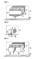
- FIG. 3 shows a perspective view of a prior art power converter
- FIG. 5 is a side view of the prior art power converter.
- IGBTs 1 are attached within a box 20 to a cooling block 4 of a semiconductor cooling unit including a cooling block 4 and a cooling fin 5, by which the heat losses are radiated to the atmosphere outside the device.
- the semiconductor cooling unit, IGBTs 1 corresponding to three phases of U, V and W and a filter capacitor 2 are stored within a single box 20, thereby constituting a power converter unit 6.
- Gate signals to the IGBTs 1 are output from gate control circuits 7 and transmitted via gate wires 8 to the respective IGBTs 1.
- the filter capacitor 2 are separated into two parts and arranged in a separated manner on left and right sides of FIG. 3 .
- the gate control circuit 7 is arranged in a space at the center of the filter capacitor 2 divided into two parts.
- the integral components including the IGBTs 1, the gate control circuits 7, the gate wires 8, the cooling unit, the conductor bar and a frame for supporting and connecting these components are specifically called a power unit.
- the power converter unit 6 having the structure shown in FIGS. 3 and 5 adopts a structure in which the filter capacitor 2 are divided into two parts and arranged on right and left sides of the unit, the thickness of the filter capacitor 2 in the front-rear direction of FIG. 3 is increased compared to a filter capacitor that is not divided into two parts.
- the gate control circuits 7 are arranged at a relatively deep position within the frame arrangement, and therefore, maintenance operations requiring visual confirmation of the gate control circuits 7 and circuit checks thereof become difficult.
- the distance between the divided filter capacitors 2 defining a maintenance space for the gate control circuits 7 is narrow, there was a drawback in that the connecting and disconnecting operation of optical fibers and the like was difficult.
- the gate control circuits corresponding to three phases are arranged collectively at the center, the gate wires 8 within the power converter unit 6 must also be collectively arranged at the center, so that it was difficult to ensure sufficient space for wiring.
- separating and binding of wires considering the influence of noise could not be performed sufficiently due to space limitation, and measures against noise could not be taken sufficiently.
- the gate control circuits 7 were arranged at the center where heat tended to gather, and especially, the gate control circuits arranged at the upper area were heated by the heat generated from the lower gate control circuits, by which the circuits were exposed to thermally hostile environment.
- the filter capacitor is divided into two parts, 2a and 2b, according to the arrangement illustrated in FIGS. 3 and 5 , the number of components related to the wire conductors and support members connected to the filter capacitor 2 was increased, causing complication of the arrangement of the device or increase of weight thereof.
- patent document 1 One arrangement for solving such problems mentioned above is disclosed for example in Japanese patent laid-open publication No. 2003-23778 (patent document 1). The arrangement disclosed in patent document 1 will be described with reference to FIG. 4 .
- IGBTs 1 are attached within a box 20 to a cooling block 4 of a semiconductor cooling unit including a cooling block 4 and a cooling fin 5, thereby radiating the heat losses to the atmospheric air outside the device.
- a power converter unit 6 is composed by storing the semiconductor cooling unit including the cooling block 4 and the cooling fin 5, a filter capacitor 2 and IGBTs 1 corresponding to three phases of U, V and W in a single box 20.
- the gate control circuits 7 are arranged side by side on a lower side of the filter capacitor 2, the gate control circuits can be accessed easily. Further, the filter capacitor is arranged above the gate control circuits as a single component without being divided.
- the filter capacitor 2 and the aforementioned power unit are arranged in a divided manner, wherein the filter capacitor 2 is fixed and supported on the box 20 before the wires of the power unit and the filter capacitor 2 are connected, so that the filter capacitor 2 and the power unit are independently fixed on the box 20.
- the power converter must be removed from the box for maintenance operation of the power converter during commercial operation of the power converter mounted on a railway rolling stock, it is necessary to remove the fixing support members between the filter capacitor and the box, disconnect wires between the filter capacitor and the unit, remove the filter capacitor from the box, remove the fixing support members between the unit and the box, and detach the unit from the box. Since the box must be arranged within a limited space under the floor of the railway vehicle, the size of the box is small, and the operation for disconnecting wires between the filter capacitor and the unit within the small box is not only very difficult but also time-consuming for operators. Further, there are a large number of steps required for removing the power converter from the box, and the operation thereof is complex.
- the filter capacitor and the unit are independently supported and fixed on the box, a large number of components such as the fixing support members is necessary, and the weight of the whole device is increased.
- the present invention aims at providing a power converter capable of improving the maintenance performance and downsizing the power converter.
- the present invention provides a power converter for a railway rolling stock comprising a plurality of semiconductor devices constituting a power converter circuit, a gate control circuit for supplying a gate signal to the semiconductor devices, and a filter capacitor connected to a DC terminal of the power converter circuit and smoothing the DC current, characterized in that the semiconductor devices and the filter capacitor are stored within a common box, and the filter capacitor and the semiconductor devices are fixed to each other to constitute an integral structure.
- the present power converter can further adopt an arrangement in which a plurality of gate control circuits are fixed to a unit frame, so as to enable the circuits to be attached to and detached from the device collectively.
- a plurality of gate control circuits are fixed to a unit frame, so as to enable the circuits to be attached to and detached from the device collectively.
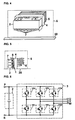
- FIG. 1 is a perspective view of a power converter according to one preferred embodiment of the present invention
- FIG. 2 is a side view of the power converter.
- the power converter comprises a power converter unit 6 corresponding collectively to three phases of U, V and W and having insulated gate type bipolar transistors (IGBTs) 1, a filter capacitor 2, a cooling block 4, a cooling fin 5 and gate control circuits 7, wherein the power converter unit 6 is stored in a fixed manner in the interior of a box 20.
- IGBTs 1 are attached to the cooling block 4 of a semiconductor cooling unit including the cooling block 4 and the cooling fin 5, and the heat loss generated from the IGBTs 1 are radiated to the atmospheric air outside the power converter.
- the gate signals to the IGBTs 1 are output from the gate control circuits 7 and transmitted via gate wires 8 to the respective IGBTs 1.
- the gate control circuits 7 are disposed on the lower side of the power converter unit 6 within the space below the bottom side of the filter capacitor 2 and on the front side of FIG. 1 (on the opposite side from the cooling fin). Moreover, the gate control circuits 7 have connecting terminals for optical fibers functioning as input ends for receiving input of signals from the exterior arranged toward the front side of FIG. 1 (not shown).
- the filter capacitor 2 is fixed to and constitutes an integral structure with the semiconductor cooling unit, the IGBTs 1 and the gate control circuits 7.
- the gate wires 8 extending from the gate control circuits 7 arranged on the lower side of the power converter unit 6 to the IGBTs 1 are arranged so that the respective phases have equivalent lengths.
- FIG. 6 is a circuit connecting diagram illustrating the traction circuit arrangement of the power converter.
- the feeding system of railways is either an AC system or a DC system
- the traction motor can be either an AC motor or a DC motor. Therefore, based on the combination of the feeding system and the motor, the power converter can adopt an inverter alone, a converter alone, or a combination of an inverter and a converter, wherein according to the present embodiment, we will described as an example an inverter applied to a combination of a DC feeding system and an AC motor.
- the traction circuit according to the present embodiment is composed of a filter capacitor 2 connected between DC terminals P and N, and a three-phase inverter 3.
- the three-phase inverter 3 is a device for converting the input DC to a three-phase AC having an arbitrary frequency and an arbitrary voltage, and outputting the three-phase AC to AC terminals U, V and W.
- Six semiconductor devices (PU, NU, PV, NV, PW, NW) of the three-phase inverter 3 are composed of IGBTs 1.
- the IGBT 1 corresponding to the respective phase is composed of a free-wheel diode connected in parallel to one device and another device. According to the structural example illustrated in the present specification, the respective semiconductor devices (PU, NU, PV, NV, PW, NW) are referred to collectively as IGBTs 1.
- the filter capacitor and the power unit are integrated as mentioned earlier, it can be attached to and removed from the box as an integral device, so that the connecting of wires within the power converter unit does not have to be performed within the box, and the connecting of wires within the power converter unit can be performed after taking out the power converter unit from the box.
- the troublesome operation within the small box can be saved, and the maintenance performance of the device can be improved.
- the filter capacitor 2 and the power unit are fixed to and supported in the box as an integral structure, they can be attached to and detached from the box as an integral device so that the number of components required to fix and support the box and the power converter unit can be reduced, the number of steps for attaching and detaching the unit from the box can be reduced, the weight of the arrangement can be reduced and the arrangement can be simplified.
- the gate control circuits 7 are arranged within the space below the lower side of the filter capacitor 2, the gate wires 8 can be arranged with equivalent lengths with respect to the IGBTs 1 of the respective phases, and the gate wires 8 can be arranged in an orderly manner in bundles without being arranged in disorder around the gate control circuits 7. Therefore, the wires can be bundled together considering measures against noise, and erroneous operations caused by noise can be prevented.
- the gate control circuits 7 are arranged close to the front side of the power converter unit 6 (on the opposite side from the cooling fin), so that during maintenance of the power converter, maintenance can be performed by accessing the various devices within the power converter unit from the front side of FIG. 1 , improving the workability of attaching and detaching the devices of the gate control circuits 7 or the optical fiber connectors, and improving the workability related to checking the gate control circuits 7.
- the gate control circuits 7 are arranged side by side in a horizontal alignment instead of being stacked one above the other in a vertical arrangement, the heat generated from the gate control circuits 7 will not affect other gate control circuits 7.
- the power converter unit including the filter capacitor 2, the semiconductor cooling unit, the IGBTs 1 and the gate control circuits 7 formed in an integral manner is fixed to the box as an integral structure, the power converter unit can be attached to and detached from the box as an integral device, so that the number of components for fixing and supporting the power converter unit on the box can be reduced, the number of steps required for attaching and detaching the unit on the box can be reduced, and the costs related to the power converter can be cut down.
- the power converter unit can be easily attached to and detached from the box as an integral device, it is not necessary to connect wires within the power converter unit inside the box, and wires within the power converter unit can be connected after removing the power converter unit from the box. In other words, it is not necessary to perform complex operations within the small box, and the maintenance performance of the power converter can be improved.
- the prior art power converter illustrated in FIG. 4 has a unit including the semiconductor devices and a filter capacitor independently fixed to the box 20, wherein the filter capacitor and the unit are connected via wires within the box. Therefore, considering the wiring operation, there was a restriction to the reduction of the distance between the filter capacitor and the unit on the circuit.
- the filter capacitor and the unit including the inverter are fixed in an integral manner, so that there is no need to perform wiring operation within the box. Therefore, the distance between the filter capacitor and the semiconductor devices on the circuit can be minimized compared to the prior art power converter, and thus, the inductance of the power converter can be reduced.
- the gate control circuits 7 are disposed on the front side on the lower side of the power converter unit 6 together with the unit frame 9.
- the unit frame 9 can be removed in an integral manner from the semiconductor cooling unit.
- the maintenance performance of the power converter can further be improved.
- a self-standing frame 10 on the lower portion of the power converter unit 6.
- the power converter unit 6 can be arranged in a self-standing manner before being fixed to the box, so that the mounting operation for attaching the unit to the box can be facilitated. Further, the handling of the power converter unit during maintenance operation can be facilitated.
Landscapes
- Engineering & Computer Science (AREA)
- Power Engineering (AREA)
- Microelectronics & Electronic Packaging (AREA)
- Physics & Mathematics (AREA)
- Thermal Sciences (AREA)
- Transportation (AREA)
- Mechanical Engineering (AREA)
- Inverter Devices (AREA)
- Electric Propulsion And Braking For Vehicles (AREA)
Applications Claiming Priority (1)
| Application Number | Priority Date | Filing Date | Title |
|---|---|---|---|
| JP2009136808A JP5549120B2 (ja) | 2009-06-08 | 2009-06-08 | 鉄道車両用の電力変換装置 |
Publications (3)
| Publication Number | Publication Date |
|---|---|
| EP2264883A2 true EP2264883A2 (fr) | 2010-12-22 |
| EP2264883A3 EP2264883A3 (fr) | 2014-12-10 |
| EP2264883B1 EP2264883B1 (fr) | 2020-01-08 |
Family
ID=42340473
Family Applications (1)
| Application Number | Title | Priority Date | Filing Date |
|---|---|---|---|
| EP10251053.4A Active EP2264883B1 (fr) | 2009-06-08 | 2010-06-08 | Convertisseur de puissance pour véhicule sur rails |
Country Status (4)
| Country | Link |
|---|---|
| EP (1) | EP2264883B1 (fr) |
| JP (1) | JP5549120B2 (fr) |
| KR (3) | KR20100131937A (fr) |
| CN (1) | CN101908817B (fr) |
Cited By (3)
| Publication number | Priority date | Publication date | Assignee | Title |
|---|---|---|---|---|
| US10075089B2 (en) | 2014-09-18 | 2018-09-11 | Kabushiki Kaisha Toshiba | Power conversion device |
| EP3667892A4 (fr) * | 2017-08-09 | 2021-04-07 | Hitachi, Ltd. | Dispositif de conversion de puissance et procédé de refroidissement associé |
| CN113172323A (zh) * | 2021-05-17 | 2021-07-27 | 重庆科技学院 | 一种用于bga锡球焊接方法及其电磁脉冲焊接设备 |
Families Citing this family (7)
| Publication number | Priority date | Publication date | Assignee | Title |
|---|---|---|---|---|
| JP2013086642A (ja) * | 2011-10-18 | 2013-05-13 | Fuji Electric Co Ltd | 車両用電力変換装置 |
| JP5875884B2 (ja) * | 2012-02-07 | 2016-03-02 | 株式会社東芝 | 電気車制御装置 |
| US9742305B2 (en) * | 2014-02-07 | 2017-08-22 | Mitsubishi Electric Corporation | Power conversion apparatus |
| JP6529868B2 (ja) * | 2015-09-09 | 2019-06-12 | 株式会社東芝 | 電動車制御装置 |
| JP6955205B2 (ja) * | 2017-09-27 | 2021-10-27 | 富士電機株式会社 | 電力変換装置 |
| JP6851300B2 (ja) * | 2017-12-20 | 2021-03-31 | 株式会社日立製作所 | 電力変換器の制御装置 |
| CN112848976A (zh) * | 2021-03-01 | 2021-05-28 | 中国铁路设计集团有限公司 | 一种基于三网融合的网络化牵引供电系统 |
Citations (1)
| Publication number | Priority date | Publication date | Assignee | Title |
|---|---|---|---|---|
| WO2003023778A1 (fr) | 2001-09-11 | 2003-03-20 | Sony Corporation | Cartouche de disque, dispositif de support d'enregistrement de disque et dispositif d'enregistrement et/ou de reproduction de disque |
Family Cites Families (18)
| Publication number | Priority date | Publication date | Assignee | Title |
|---|---|---|---|---|
| JPH05260763A (ja) * | 1992-03-12 | 1993-10-08 | Fuji Electric Co Ltd | 板金構造のインバータ装置 |
| JP3565181B2 (ja) * | 1995-06-28 | 2004-09-15 | 富士電機デバイステクノロジー株式会社 | 高耐圧ic |
| JPH1189248A (ja) * | 1997-09-02 | 1999-03-30 | Denso Corp | 電力制御装置 |
| JP4512211B2 (ja) * | 1999-01-25 | 2010-07-28 | 株式会社日立産機システム | 電流制御回路、インバータ制御装置、インバータ装置、および電力変換装置 |
| JP2001061282A (ja) * | 1999-08-19 | 2001-03-06 | Meidensha Corp | インバータ装置 |
| JP2001086732A (ja) * | 1999-09-13 | 2001-03-30 | Toshiba Transport Eng Inc | 電力変換装置 |
| JP3484122B2 (ja) * | 2000-01-13 | 2004-01-06 | 三菱電機株式会社 | 電力変換装置 |
| JP3649133B2 (ja) * | 2001-02-06 | 2005-05-18 | 株式会社日立製作所 | パワーモジュール |
| JP4439764B2 (ja) * | 2001-07-05 | 2010-03-24 | 東芝トランスポートエンジニアリング株式会社 | 車両用電力変換装置 |
| JP3906141B2 (ja) * | 2001-12-07 | 2007-04-18 | 東芝トランスポートエンジニアリング株式会社 | 電力変換装置 |
| US6965514B2 (en) * | 2002-01-16 | 2005-11-15 | Rockwell Automation Technologies, Inc. | Fluid cooled vehicle drive module |
| CN101685028B (zh) * | 2002-09-20 | 2011-09-21 | 矢崎总业株式会社 | 连接器组件以及使用了该组件的仪表 |
| JP2005229708A (ja) * | 2004-02-12 | 2005-08-25 | Toshiba Corp | 鉄道車両用電力変換装置 |
| JP4502849B2 (ja) * | 2005-03-14 | 2010-07-14 | 三菱電機株式会社 | 鉄道車両用の電力変換装置 |
| JP4931458B2 (ja) * | 2006-04-06 | 2012-05-16 | 日立オートモティブシステムズ株式会社 | 電力変換装置 |
| JP4452952B2 (ja) * | 2007-06-20 | 2010-04-21 | 日立オートモティブシステムズ株式会社 | 電力変換装置 |
| JP4452953B2 (ja) * | 2007-08-09 | 2010-04-21 | 日立オートモティブシステムズ株式会社 | 電力変換装置 |
| JP5148238B2 (ja) * | 2007-10-16 | 2013-02-20 | 東海旅客鉄道株式会社 | 高速鉄道車両用電力変換装置 |
-
2009
- 2009-06-08 JP JP2009136808A patent/JP5549120B2/ja active Active
-
2010
- 2010-06-07 CN CN201010198834XA patent/CN101908817B/zh active Active
- 2010-06-07 KR KR1020100053367A patent/KR20100131937A/ko not_active Ceased
- 2010-06-08 EP EP10251053.4A patent/EP2264883B1/fr active Active
-
2012
- 2012-06-05 KR KR1020120060143A patent/KR101304838B1/ko active Active
-
2013
- 2013-07-23 KR KR1020130086649A patent/KR101317587B1/ko active Active
Patent Citations (1)
| Publication number | Priority date | Publication date | Assignee | Title |
|---|---|---|---|---|
| WO2003023778A1 (fr) | 2001-09-11 | 2003-03-20 | Sony Corporation | Cartouche de disque, dispositif de support d'enregistrement de disque et dispositif d'enregistrement et/ou de reproduction de disque |
Cited By (3)
| Publication number | Priority date | Publication date | Assignee | Title |
|---|---|---|---|---|
| US10075089B2 (en) | 2014-09-18 | 2018-09-11 | Kabushiki Kaisha Toshiba | Power conversion device |
| EP3667892A4 (fr) * | 2017-08-09 | 2021-04-07 | Hitachi, Ltd. | Dispositif de conversion de puissance et procédé de refroidissement associé |
| CN113172323A (zh) * | 2021-05-17 | 2021-07-27 | 重庆科技学院 | 一种用于bga锡球焊接方法及其电磁脉冲焊接设备 |
Also Published As
| Publication number | Publication date |
|---|---|
| KR101304838B1 (ko) | 2013-09-05 |
| JP2010284049A (ja) | 2010-12-16 |
| KR20120069644A (ko) | 2012-06-28 |
| EP2264883A3 (fr) | 2014-12-10 |
| CN101908817A (zh) | 2010-12-08 |
| KR20130093058A (ko) | 2013-08-21 |
| KR101317587B1 (ko) | 2013-10-11 |
| EP2264883B1 (fr) | 2020-01-08 |
| CN101908817B (zh) | 2013-10-30 |
| KR20100131937A (ko) | 2010-12-16 |
| JP5549120B2 (ja) | 2014-07-16 |
Similar Documents
| Publication | Publication Date | Title |
|---|---|---|
| EP2264883A2 (fr) | Convertisseur de puissance pour véhicule sur rails | |
| EP1950879B1 (fr) | Système de commande de moteur pour véhicule ferroviaire | |
| US20140345492A1 (en) | Drive control equipment for a vehicle | |
| JP6429721B2 (ja) | 電力変換装置及び鉄道車両 | |
| EP2482438A2 (fr) | Transformateur électrique | |
| KR102194361B1 (ko) | 전기 기기와 그 제조 방법 | |
| WO2019026339A1 (fr) | Dispositif de conversion de courant et véhicule équipé du dispositif de conversion de courant | |
| EP2343227B1 (fr) | Dispositif de commande de véhicule du type refroidi par air forcé | |
| EP3745579B1 (fr) | Dispositif de conversion de puissance et véhicule ferroviaire électrique équipé du dispositif de conversion de puissance | |
| JP2019033587A (ja) | 電力変換装置および電力変換装置を搭載した車両 | |
| US20210021152A1 (en) | Uninterruptible power supply | |
| CN107949980A (zh) | 电压转换器,电的驱动系统和用于减小干扰电压的方法 | |
| US11929687B2 (en) | Power converter | |
| CN106464145B (zh) | 矩阵变换器 | |
| JP5550572B2 (ja) | 電力変換装置 | |
| JP4439764B2 (ja) | 車両用電力変換装置 | |
| CN105305834A (zh) | 电容器模块以及矩阵变换器 | |
| JP2020156206A (ja) | 電力変換器 | |
| JP2015076933A (ja) | 電力変換装置 | |
| JP6604097B2 (ja) | スイッチング回路および電力変換装置 | |
| US20250266756A1 (en) | Power conversion device | |
| JP2017212333A (ja) | 基板支持ブラケット | |
| JP2006254656A (ja) | 鉄道車両用の電力変換装置 | |
| JP2019161749A (ja) | 電力変換装置 | |
| JP2011036029A (ja) | 電力変換装置 |
Legal Events
| Date | Code | Title | Description |
|---|---|---|---|
| PUAI | Public reference made under article 153(3) epc to a published international application that has entered the european phase |
Free format text: ORIGINAL CODE: 0009012 |
|
| 17P | Request for examination filed |
Effective date: 20100625 |
|
| AK | Designated contracting states |
Kind code of ref document: A2 Designated state(s): AL AT BE BG CH CY CZ DE DK EE ES FI FR GB GR HR HU IE IS IT LI LT LU LV MC MK MT NL NO PL PT RO SE SI SK SM TR |
|
| AX | Request for extension of the european patent |
Extension state: BA ME RS |
|
| RIN1 | Information on inventor provided before grant (corrected) |
Inventor name: TANAKA, TAKESHI Inventor name: NAKATA, KIYOSHI Inventor name: YAMAGUCHI, SATOSHI Inventor name: KONO, YASUHIKO Inventor name: HISHIDA, AKIHIRO |
|
| PUAL | Search report despatched |
Free format text: ORIGINAL CODE: 0009013 |
|
| AK | Designated contracting states |
Kind code of ref document: A3 Designated state(s): AL AT BE BG CH CY CZ DE DK EE ES FI FR GB GR HR HU IE IS IT LI LT LU LV MC MK MT NL NO PL PT RO SE SI SK SM TR |
|
| AX | Request for extension of the european patent |
Extension state: BA ME RS |
|
| RIC1 | Information provided on ipc code assigned before grant |
Ipc: H05K 5/02 20060101ALI20141105BHEP Ipc: H02M 7/00 20060101AFI20141105BHEP |
|
| RBV | Designated contracting states (corrected) |
Designated state(s): AL AT BE BG CH CY CZ DE DK EE ES FI FR GB GR HR HU IE IS IT LI LT LU LV MC MK MT NL NO PL PT RO SE SI SK SM TR |
|
| STAA | Information on the status of an ep patent application or granted ep patent |
Free format text: STATUS: EXAMINATION IS IN PROGRESS |
|
| 17Q | First examination report despatched |
Effective date: 20171211 |
|
| GRAP | Despatch of communication of intention to grant a patent |
Free format text: ORIGINAL CODE: EPIDOSNIGR1 |
|
| STAA | Information on the status of an ep patent application or granted ep patent |
Free format text: STATUS: GRANT OF PATENT IS INTENDED |
|
| INTG | Intention to grant announced |
Effective date: 20190814 |
|
| GRAS | Grant fee paid |
Free format text: ORIGINAL CODE: EPIDOSNIGR3 |
|
| GRAA | (expected) grant |
Free format text: ORIGINAL CODE: 0009210 |
|
| STAA | Information on the status of an ep patent application or granted ep patent |
Free format text: STATUS: THE PATENT HAS BEEN GRANTED |
|
| AK | Designated contracting states |
Kind code of ref document: B1 Designated state(s): AL AT BE BG CH CY CZ DE DK EE ES FI FR GB GR HR HU IE IS IT LI LT LU LV MC MK MT NL NO PL PT RO SE SI SK SM TR |
|
| REG | Reference to a national code |
Ref country code: GB Ref legal event code: FG4D |
|
| REG | Reference to a national code |
Ref country code: CH Ref legal event code: EP |
|
| REG | Reference to a national code |
Ref country code: DE Ref legal event code: R096 Ref document number: 602010062699 Country of ref document: DE |
|
| REG | Reference to a national code |
Ref country code: IE Ref legal event code: FG4D |
|
| REG | Reference to a national code |
Ref country code: AT Ref legal event code: REF Ref document number: 1223913 Country of ref document: AT Kind code of ref document: T Effective date: 20200215 |
|
| REG | Reference to a national code |
Ref country code: NL Ref legal event code: MP Effective date: 20200108 |
|
| REG | Reference to a national code |
Ref country code: LT Ref legal event code: MG4D |
|
| PG25 | Lapsed in a contracting state [announced via postgrant information from national office to epo] |
Ref country code: FI Free format text: LAPSE BECAUSE OF FAILURE TO SUBMIT A TRANSLATION OF THE DESCRIPTION OR TO PAY THE FEE WITHIN THE PRESCRIBED TIME-LIMIT Effective date: 20200108 Ref country code: NO Free format text: LAPSE BECAUSE OF FAILURE TO SUBMIT A TRANSLATION OF THE DESCRIPTION OR TO PAY THE FEE WITHIN THE PRESCRIBED TIME-LIMIT Effective date: 20200408 Ref country code: LT Free format text: LAPSE BECAUSE OF FAILURE TO SUBMIT A TRANSLATION OF THE DESCRIPTION OR TO PAY THE FEE WITHIN THE PRESCRIBED TIME-LIMIT Effective date: 20200108 Ref country code: NL Free format text: LAPSE BECAUSE OF FAILURE TO SUBMIT A TRANSLATION OF THE DESCRIPTION OR TO PAY THE FEE WITHIN THE PRESCRIBED TIME-LIMIT Effective date: 20200108 Ref country code: PT Free format text: LAPSE BECAUSE OF FAILURE TO SUBMIT A TRANSLATION OF THE DESCRIPTION OR TO PAY THE FEE WITHIN THE PRESCRIBED TIME-LIMIT Effective date: 20200531 |
|
| PG25 | Lapsed in a contracting state [announced via postgrant information from national office to epo] |
Ref country code: GR Free format text: LAPSE BECAUSE OF FAILURE TO SUBMIT A TRANSLATION OF THE DESCRIPTION OR TO PAY THE FEE WITHIN THE PRESCRIBED TIME-LIMIT Effective date: 20200409 Ref country code: IS Free format text: LAPSE BECAUSE OF FAILURE TO SUBMIT A TRANSLATION OF THE DESCRIPTION OR TO PAY THE FEE WITHIN THE PRESCRIBED TIME-LIMIT Effective date: 20200508 Ref country code: HR Free format text: LAPSE BECAUSE OF FAILURE TO SUBMIT A TRANSLATION OF THE DESCRIPTION OR TO PAY THE FEE WITHIN THE PRESCRIBED TIME-LIMIT Effective date: 20200108 Ref country code: LV Free format text: LAPSE BECAUSE OF FAILURE TO SUBMIT A TRANSLATION OF THE DESCRIPTION OR TO PAY THE FEE WITHIN THE PRESCRIBED TIME-LIMIT Effective date: 20200108 Ref country code: SE Free format text: LAPSE BECAUSE OF FAILURE TO SUBMIT A TRANSLATION OF THE DESCRIPTION OR TO PAY THE FEE WITHIN THE PRESCRIBED TIME-LIMIT Effective date: 20200108 Ref country code: BG Free format text: LAPSE BECAUSE OF FAILURE TO SUBMIT A TRANSLATION OF THE DESCRIPTION OR TO PAY THE FEE WITHIN THE PRESCRIBED TIME-LIMIT Effective date: 20200408 |
|
| REG | Reference to a national code |
Ref country code: DE Ref legal event code: R097 Ref document number: 602010062699 Country of ref document: DE |
|
| PG25 | Lapsed in a contracting state [announced via postgrant information from national office to epo] |
Ref country code: ES Free format text: LAPSE BECAUSE OF FAILURE TO SUBMIT A TRANSLATION OF THE DESCRIPTION OR TO PAY THE FEE WITHIN THE PRESCRIBED TIME-LIMIT Effective date: 20200108 Ref country code: CZ Free format text: LAPSE BECAUSE OF FAILURE TO SUBMIT A TRANSLATION OF THE DESCRIPTION OR TO PAY THE FEE WITHIN THE PRESCRIBED TIME-LIMIT Effective date: 20200108 Ref country code: RO Free format text: LAPSE BECAUSE OF FAILURE TO SUBMIT A TRANSLATION OF THE DESCRIPTION OR TO PAY THE FEE WITHIN THE PRESCRIBED TIME-LIMIT Effective date: 20200108 Ref country code: EE Free format text: LAPSE BECAUSE OF FAILURE TO SUBMIT A TRANSLATION OF THE DESCRIPTION OR TO PAY THE FEE WITHIN THE PRESCRIBED TIME-LIMIT Effective date: 20200108 Ref country code: SM Free format text: LAPSE BECAUSE OF FAILURE TO SUBMIT A TRANSLATION OF THE DESCRIPTION OR TO PAY THE FEE WITHIN THE PRESCRIBED TIME-LIMIT Effective date: 20200108 Ref country code: DK Free format text: LAPSE BECAUSE OF FAILURE TO SUBMIT A TRANSLATION OF THE DESCRIPTION OR TO PAY THE FEE WITHIN THE PRESCRIBED TIME-LIMIT Effective date: 20200108 Ref country code: SK Free format text: LAPSE BECAUSE OF FAILURE TO SUBMIT A TRANSLATION OF THE DESCRIPTION OR TO PAY THE FEE WITHIN THE PRESCRIBED TIME-LIMIT Effective date: 20200108 |
|
| PLBE | No opposition filed within time limit |
Free format text: ORIGINAL CODE: 0009261 |
|
| STAA | Information on the status of an ep patent application or granted ep patent |
Free format text: STATUS: NO OPPOSITION FILED WITHIN TIME LIMIT |
|
| REG | Reference to a national code |
Ref country code: AT Ref legal event code: MK05 Ref document number: 1223913 Country of ref document: AT Kind code of ref document: T Effective date: 20200108 |
|
| 26N | No opposition filed |
Effective date: 20201009 |
|
| PG25 | Lapsed in a contracting state [announced via postgrant information from national office to epo] |
Ref country code: MC Free format text: LAPSE BECAUSE OF FAILURE TO SUBMIT A TRANSLATION OF THE DESCRIPTION OR TO PAY THE FEE WITHIN THE PRESCRIBED TIME-LIMIT Effective date: 20200108 Ref country code: AT Free format text: LAPSE BECAUSE OF FAILURE TO SUBMIT A TRANSLATION OF THE DESCRIPTION OR TO PAY THE FEE WITHIN THE PRESCRIBED TIME-LIMIT Effective date: 20200108 |
|
| REG | Reference to a national code |
Ref country code: CH Ref legal event code: PL |
|
| PG25 | Lapsed in a contracting state [announced via postgrant information from national office to epo] |
Ref country code: PL Free format text: LAPSE BECAUSE OF FAILURE TO SUBMIT A TRANSLATION OF THE DESCRIPTION OR TO PAY THE FEE WITHIN THE PRESCRIBED TIME-LIMIT Effective date: 20200108 Ref country code: SI Free format text: LAPSE BECAUSE OF FAILURE TO SUBMIT A TRANSLATION OF THE DESCRIPTION OR TO PAY THE FEE WITHIN THE PRESCRIBED TIME-LIMIT Effective date: 20200108 |
|
| PG25 | Lapsed in a contracting state [announced via postgrant information from national office to epo] |
Ref country code: LU Free format text: LAPSE BECAUSE OF NON-PAYMENT OF DUE FEES Effective date: 20200608 |
|
| REG | Reference to a national code |
Ref country code: BE Ref legal event code: MM Effective date: 20200630 |
|
| PG25 | Lapsed in a contracting state [announced via postgrant information from national office to epo] |
Ref country code: FR Free format text: LAPSE BECAUSE OF NON-PAYMENT OF DUE FEES Effective date: 20200630 Ref country code: LI Free format text: LAPSE BECAUSE OF NON-PAYMENT OF DUE FEES Effective date: 20200630 Ref country code: IE Free format text: LAPSE BECAUSE OF NON-PAYMENT OF DUE FEES Effective date: 20200608 Ref country code: CH Free format text: LAPSE BECAUSE OF NON-PAYMENT OF DUE FEES Effective date: 20200630 |
|
| PG25 | Lapsed in a contracting state [announced via postgrant information from national office to epo] |
Ref country code: BE Free format text: LAPSE BECAUSE OF NON-PAYMENT OF DUE FEES Effective date: 20200630 |
|
| PG25 | Lapsed in a contracting state [announced via postgrant information from national office to epo] |
Ref country code: TR Free format text: LAPSE BECAUSE OF FAILURE TO SUBMIT A TRANSLATION OF THE DESCRIPTION OR TO PAY THE FEE WITHIN THE PRESCRIBED TIME-LIMIT Effective date: 20200108 Ref country code: MT Free format text: LAPSE BECAUSE OF FAILURE TO SUBMIT A TRANSLATION OF THE DESCRIPTION OR TO PAY THE FEE WITHIN THE PRESCRIBED TIME-LIMIT Effective date: 20200108 Ref country code: CY Free format text: LAPSE BECAUSE OF FAILURE TO SUBMIT A TRANSLATION OF THE DESCRIPTION OR TO PAY THE FEE WITHIN THE PRESCRIBED TIME-LIMIT Effective date: 20200108 |
|
| PG25 | Lapsed in a contracting state [announced via postgrant information from national office to epo] |
Ref country code: MK Free format text: LAPSE BECAUSE OF FAILURE TO SUBMIT A TRANSLATION OF THE DESCRIPTION OR TO PAY THE FEE WITHIN THE PRESCRIBED TIME-LIMIT Effective date: 20200108 Ref country code: AL Free format text: LAPSE BECAUSE OF FAILURE TO SUBMIT A TRANSLATION OF THE DESCRIPTION OR TO PAY THE FEE WITHIN THE PRESCRIBED TIME-LIMIT Effective date: 20200108 |
|
| PGFP | Annual fee paid to national office [announced via postgrant information from national office to epo] |
Ref country code: DE Payment date: 20250429 Year of fee payment: 16 |
|
| PGFP | Annual fee paid to national office [announced via postgrant information from national office to epo] |
Ref country code: GB Payment date: 20250501 Year of fee payment: 16 |
|
| PGFP | Annual fee paid to national office [announced via postgrant information from national office to epo] |
Ref country code: IT Payment date: 20250522 Year of fee payment: 16 |