EP2264889A2 - Procédé et appareil de contrôle d'alimentation d'un amplificateur audio - Google Patents
Procédé et appareil de contrôle d'alimentation d'un amplificateur audio Download PDFInfo
- Publication number
- EP2264889A2 EP2264889A2 EP10166216A EP10166216A EP2264889A2 EP 2264889 A2 EP2264889 A2 EP 2264889A2 EP 10166216 A EP10166216 A EP 10166216A EP 10166216 A EP10166216 A EP 10166216A EP 2264889 A2 EP2264889 A2 EP 2264889A2
- Authority
- EP
- European Patent Office
- Prior art keywords
- audio
- level
- power supply
- value
- power
- Prior art date
- Legal status (The legal status is an assumption and is not a legal conclusion. Google has not performed a legal analysis and makes no representation as to the accuracy of the status listed.)
- Withdrawn
Links
Images


Classifications
-
- H—ELECTRICITY
- H03—ELECTRONIC CIRCUITRY
- H03F—AMPLIFIERS
- H03F1/00—Details of amplifiers with only discharge tubes, only semiconductor devices or only unspecified devices as amplifying elements
- H03F1/02—Modifications of amplifiers to raise the efficiency, e.g. gliding Class A stages, use of an auxiliary oscillation
- H03F1/0205—Modifications of amplifiers to raise the efficiency, e.g. gliding Class A stages, use of an auxiliary oscillation in transistor amplifiers
- H03F1/0211—Modifications of amplifiers to raise the efficiency, e.g. gliding Class A stages, use of an auxiliary oscillation in transistor amplifiers with control of the supply voltage or current
- H03F1/0216—Continuous control
- H03F1/0222—Continuous control by using a signal derived from the input signal
-
- H—ELECTRICITY
- H03—ELECTRONIC CIRCUITRY
- H03F—AMPLIFIERS
- H03F1/00—Details of amplifiers with only discharge tubes, only semiconductor devices or only unspecified devices as amplifying elements
- H03F1/02—Modifications of amplifiers to raise the efficiency, e.g. gliding Class A stages, use of an auxiliary oscillation
- H03F1/0205—Modifications of amplifiers to raise the efficiency, e.g. gliding Class A stages, use of an auxiliary oscillation in transistor amplifiers
- H03F1/0211—Modifications of amplifiers to raise the efficiency, e.g. gliding Class A stages, use of an auxiliary oscillation in transistor amplifiers with control of the supply voltage or current
- H03F1/0244—Stepped control
- H03F1/025—Stepped control by using a signal derived from the input signal
-
- H—ELECTRICITY
- H03—ELECTRONIC CIRCUITRY
- H03F—AMPLIFIERS
- H03F3/00—Amplifiers with only discharge tubes or only semiconductor devices as amplifying elements
- H03F3/20—Power amplifiers, e.g. Class B amplifiers, Class C amplifiers
- H03F3/21—Power amplifiers, e.g. Class B amplifiers, Class C amplifiers with semiconductor devices only
- H03F3/217—Class D power amplifiers; Switching amplifiers
-
- H—ELECTRICITY
- H03—ELECTRONIC CIRCUITRY
- H03F—AMPLIFIERS
- H03F2200/00—Indexing scheme relating to amplifiers
- H03F2200/03—Indexing scheme relating to amplifiers the amplifier being designed for audio applications
-
- H—ELECTRICITY
- H03—ELECTRONIC CIRCUITRY
- H03F—AMPLIFIERS
- H03F2200/00—Indexing scheme relating to amplifiers
- H03F2200/351—Pulse width modulation being used in an amplifying circuit
-
- H—ELECTRICITY
- H03—ELECTRONIC CIRCUITRY
- H03F—AMPLIFIERS
- H03F2200/00—Indexing scheme relating to amplifiers
- H03F2200/507—A switch being used for switching on or off a supply or supplying circuit in an IC-block amplifier circuit
-
- H—ELECTRICITY
- H03—ELECTRONIC CIRCUITRY
- H03F—AMPLIFIERS
- H03F2200/00—Indexing scheme relating to amplifiers
- H03F2200/511—Many discrete supply voltages or currents or voltage levels can be chosen by a control signal in an IC-block amplifier circuit
Definitions
- Apparatuses and methods consistent with the present invention relate to a digital audio amplifier system, and more particularly, to a method and apparatus for controlling a power supply of an audio amplifier by changing the power supply voltage supplied to a power switching circuit unit of the audio amplifier.
- Class-D audio amplifiers may prevent amplification efficiency reduction caused in class-A, class-B, and class-AB audio amplifiers.
- Class-D audio amplifiers are classified as open loop type or closed-loop type, and change an audio signal into a pulse width modulation (PWM) signal.
- PWM pulse width modulation
- a class-D audio amplifier generally drives a power switching circuit by using a high fixed power value corresponding to a maximum audio output.
- the class-D audio amplifier that operates at high power may cause device heating or generate noise in neighboring electronic devices.
- the present invention provides a method and apparatus for variably controlling power supply voltage of an audio amplifier according to an input audio signal level.
- a method of controlling power supply voltage of an audio amplifier including estimating, with a digital signal processor, an audio output level of an input audio signal based on correlations between the input audio signal level and audio level change factors; setting a value of power supply voltage supplied to a power switching circuit unit in correspondence with the estimated audio output level; and amplifying an audio output signal by variably controlling the power supply voltage supplied to the power switching circuit unit according to the set value of power supply voltage.
- an apparatus for controlling power supply of an audio amplifier including a digital signal processor which estimates an audio output level based on correlations between an input audio signal level and audio level change factors, and sets a power control value corresponding to the estimated audio output level; a variable power supply unit which supplies a voltage that is variable according to the power control value set by the digital signal processor; and a power switching circuit unit for which amplifies a pulse width modulation signal according to variable voltage supplied by the variable power supply unit.
- the digital signal processor may include a signal level detection unit which detects audio signal levels of a plurality of channels; an output change factor analysis unit which analyzes audio level change factors regarding an audio output by using a volume level value and gain values of the audio amplifier; an audio output estimation unit which estimates an audio output level based on correlations between the audio signal level detected by the signal level detection unit and the audio level change factors analyzed by the output change factor analysis unit; and a power control value generation unit which sets a power control value corresponding to the audio output level estimated by the audio output estimation unit.
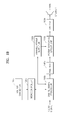
- FIG. 1A is a block diagram of a closed-loop type class-D audio amplifier system according to an exemplary embodiment of the present invention
- FIG. 1B is a block diagram of a open-loop type class-D audio amplifier system according to an exemplary embodiment of the present invention
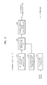
- FIG. 2 is a detailed block diagram of a digital signal processor illustrated in FIG. 1A or 1B ;
- FIG. 3 is a circuit diagram of a power switching circuit unit and a low pass filter (LPF) illustrated in FIG. 1A or 1B ;
- LPF low pass filter
- FIG. 4 is a flowchart of a method of controlling power supply voltage of a closed-loop type class-D audio amplifier, according to an exemplary embodiment of the present invention
- FIG. 5 is a flowchart of a method of controlling power supply voltage of a closed-loop type class-D audio amplifier, according to another exemplary embodiment of the present invention.
- FIG. 6 is a flowchart of a method of controlling power supply voltage of an open-loop type class-D audio amplifier, according to an exemplary embodiment of the present invention
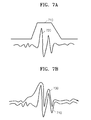
- FIGS. 7A and 7B are waveforms showing correlations between an audio signal output and power supply voltage, according to exemplary embodiments of the present invention.
- FIGS. 8A and 8B illustrate waveforms of a power control signal that follows an audio output in order to prevent audio output distortion in the digital signal processor illustrated in FIG. 1A or 1B , according to an exemplary embodiment of the present invention.
- FIGS. 9A and 9B are graphs showing power control comparison between an audio amplifier according to an exemplary embodiment of the present invention and a related art audio amplifier.
- FIG. 1A is a block diagram of a closed-loop type class-D audio amplifier system according to an exemplary embodiment of the present invention.
- the closed-loop type class-D audio amplifier system when power supply voltage is changed, the closed-loop type class-D audio amplifier system simultaneously changes the duty and the amplitude of a pulse width modulation (PWM) signal supplied by the PWM unit 140a.
- PWM pulse width modulation
- the closed-loop type class-D audio amplifier system includes a volume change unit 110a, a microcontroller 120a, a digital signal processor 130a, a PWM unit 140a, a variable power supply unit 150a, a power switching circuit unit 160a, a feedback unit 170a, a low pass filter (LPF) unit 180a, and a speaker 190a.
- An analog or digital audio signal having a plurality of channels is input to the closed-loop type class-D audio amplifier system.
- the volume change unit 110a may be part of a remote controller or a display panel and generates volume key information according to a volume key selected by a user.
- the microcontroller 120a When the volume key information is received by the microcontroller 120a, the microcontroller 120a converts the volume key information into a volume level value. Also, the microcontroller 120a loads internal gain values of the closed-loop type class-D audio amplifier system, which affect an audio output.
- the internal gain values may include, but are not limited to, gain values of the digital signal processor 130a and the PWM unit 140a.
- the microcontroller 120a initially sets the gain values of the digital signal processor 130a and the PWM unit 140a according to the number of channels of the input audio signal, and, when a reproduction operation is performed, transmits the gain values to the digital signal processor 130a and the PWM unit 140a.
- the digital signal processor 130a converts the input audio signal into pulse code modulated (PCM) audio data according to a control signal of the microcontroller 120a.
- PCM pulse code modulated
- the digital signal processor 130a analyzes audio level change factors that affect an audio output, for example, but not limited to, the volume level value and the internal gain values of the closed-loop type class-D audio amplifier system, which are input from the microcontroller 120a.
- the digital signal processor 130a also estimates an audio output level based on correlations between the input audio signal level and the audio level change factors, and sets the power supply voltage supplied to the power switching circuit unit 160a in correspondence with the estimated audio output level.
- the digital signal processor 130a outputs a power control signal corresponding to the estimated audio output level, to the variable power supply unit 150a.
- the power control signal causes the variable power supply unit 150a to adjust the power supply voltage supplied to the power switching circuit unit 160a prior to output of the audio signal on which the estimated audio output level is based.
- the digital signal processor 130a may process the power control signal to be transmitted to the variable power supply unit 150a, by using a stepped method or a linear method.
- the digital signal processor 130a transmits a power control signal that matches a reference value of each step, to the variable power supply unit 150a.
- the digital signal processor 130a transmits a linear value that is proportional to the level of an audio signal output without a reference value of each step, to the variable power supply unit 150a.
- the digital signal processor 130a adjusts a tracking time of the power control signal with respect to the output audio signal so as to prevent sound quality distortion due to output audio signal clipping caused by insufficient power supply voltage.
- the PWM unit 140a compares the level of a carrier signal to the level of the PCM audio data output from the digital signal processor 130a and generates a low-power PWM signal.
- the variable power supply unit 150a supplies a variable voltage corresponding to a power control value input from the digital signal processor 130a, to the power switching circuit unit 160a.
- the variable power supply unit 150a may be realized by using a resistance ratio.
- the power switching circuit unit 160a power-amplifies the low-power PWM signal generated by the PWM unit 140a into a high-power PWM signal according to the variable voltage supplied from the variable power supply unit 150a. According to an exemplary embodiment of the present invention, the power switching circuit unit 160a amplifies a low-power PWM signal of 3.3V into a high-power PWM signal of 5V to 40V.
- a low-power PWM signal of 3.3V into a high-power PWM signal of 5V to 40V
- the feedback unit 170a feeds a portion of the high-power PWM signal output from the power switching circuit unit 160a back to the power switching circuit unit 160a in order to correct an error between input and output signals of the power switching circuit unit 160a.
- the LPF 180a removes noise and restores an original audio signal by low-pass-filtering the high-power PWM signal power-amplified by the power switching circuit unit 160a.
- the speaker 190a reproduces the audio signal outputted by the LPF 180a as sound.
- FIG. 1B is a block diagram of an open-loop type class-D audio amplifier system according to an exemplary embodiment of the present invention.
- the open-loop type class-D audio amplifier system changes the amplitude of a PWM signal supplied by the PWM unit 140b while maintaining the duty of the PWM signal.
- an audio output of the open-loop type class-D audio amplifier system is changed according to a power supply voltage change.
- the open-loop type class-D audio amplifier system has to adjust a reference volume by a value corresponding to the changed power supply voltage in order to maintain the magnitude of an output signal against the power supply voltage change.
- the open-loop type class-D audio amplifier system may be realized by excluding the feedback unit 170a from the closed-loop type class-D audio amplifier system illustrated in FIG. 1A .
- the open-loop type class-D audio amplifier system includes a volume change unit 110b, a microcontroller 120b, a digital signal processor 130b, a PWM unit 140b, a variable power supply unit 150b, a power switching circuit unit 160b, an LPF 180b, and a speaker 190b.
- the volume change unit 110b, the microcontroller 120b, the PWM unit 140b, the variable power supply unit 150b, the power switching circuit unit 160b, the LPF 180b, and the speaker 190b operate similarly to the volume change unit 110a, the microcontroller 120a, the PWM unit 140a, the variable power supply unit 150a, the power switching circuit unit 160a, the LPF 180a, and the speaker 190a illustrated in FIG. 1A , and thus descriptions thereof will be omitted here.
- the digital signal processor 130b estimates an audio output level based on correlations between an input audio signal level and audio level change factors, sets the power supply voltage to the power switching circuit unit 160b in correspondence with the estimated audio output level, and outputs to the variable power supply unit 150b a power control signal corresponding to the estimated audio output level.
- the power control signal causes the variable power supply unit 150b to adjust the power supply voltage supplied to the power switching circuit unit 160b prior to output of the audio signal.
- the digital signal processor 130b associates a reference volume (digital gain) with a power value. That is, the digital signal processor 130b changes a power supply voltage value in correspondence with the estimated audio output level and adjusts the reference volume (digital gain) by the changed power supply voltage value in order to maintain the magnitude of an output signal against a power supply voltage change.
- FIG. 2 is a detailed block diagram of the digital signal processor 130a or 130b illustrated in FIG. 1A or 1B .
- FIG. 2 will be described in conjunction with FIGS. 1A and 1B .
- the digital signal processor 130a or 130b includes an audio signal processor 210, an audio signal level detection unit 220, an output change factor analysis unit 230, an audio output estimation unit 250, and a power control value generation unit 260.
- the audio signal processor 210 converts an input audio signal having a plurality of channels into PCM audio data, and performs signal processing, for example, but not limited to, equalization and enhancement on the PCM audio data.
- the audio signal level detection unit 220 detects peak-to-peak values of the PCM audio data that is signal-processed by the audio signal processor 210.
- the output change factor analysis unit 230 analyzes audio level change factors that affect an audio output, for example, but not limited to, volume level value and internal gain values of an audio amplifier, which are input from the microcontroller 120a or 120b.
- the audio output estimation unit 250 selects the largest audio signal level from among audio signal levels detected by the audio signal level detection unit 220, and estimates an audio output level based on correlations between the selected audio signal level and the audio level change factors analyzed by the output change factor analysis unit 230. For example, the estimated audio output level is obtained by multiplying the input audio signal level by the volume level value and the internal gain values of the audio amplifier.
- the power control value generation unit 260 initially sets a power control value corresponding to the audio output level, which is estimated by the audio output estimation unit 250, and outputs the power control value to the variable power supply unit 150a and 150b.
- the power control value generation unit 260 generates different power control values according to an open-loop type and a closed-loop type amplifier configuration.
- FIG. 3 is a circuit diagram of the power switching circuit unit 160a or 160b and the LPF 180a or 180b illustrated in FIG. 1A or 1B .
- the power switching circuit unit 160a or 160b includes a p-type metal-oxide semiconductor (PMOS) transistor P1 and an n-type metal-oxide semiconductor (NMOS) transistor N1.
- a PWM signal is divided into first and second PWM signals Q1 and Q2, respectively, having the same phase.
- the PMOS transistor P1 is switched according to the first PWM signal Q1, and an actual power supply voltage VCC2 is applied to a source of the PMOS transistor P1.
- the NMOS transistor N1 is switched according to the second PWM signal Q2, a drain of the NMOS transistor N1 is connected to a drain of the PMOS transistor P1, and a source of the NMOS transistor N1 is connected to an actual ground voltage VSS2.
- PMOS p-type metal-oxide semiconductor
- NMOS n-type metal-oxide semiconductor
- VCC1 and VSS1 represent ideal voltages applied from voltage sources, and VCC2 and VSS2 are dropped by certain values due to resistances of wires 50 that connect the voltage sources to the power switching circuit unit 160a or 160b, and represent actual voltages applied to the power switching circuit unit 160a or 160b.
- R1 and R2 represent the resistances of the wires 50 between the voltage sources and the power switching circuit unit 160a or 160b.
- the power switching circuit unit 160a or 160b may be formed with only NMOS transistors.
- the LPF 180a or 180b includes an inductor 32 and a capacitor 34.
- the LPF 180a or 180b removes a high-frequency component of the PWM signal output from the power switching circuit unit 160a or 160b.
- FIG. 4 is a flowchart of a method of controlling power supply voltage of a closed-loop type class-D audio amplifier, according to an exemplary embodiment of the present invention.
- FIG. 7A is a waveform showing correlations between an audio signal output and power supply voltage, according to an exemplary embodiment of the present invention.
- audio signal levels of an audio signal input through a plurality of channels are detected (410).
- An audio volume level set for example, by a user using a remote controller, is obtained (420).
- Audio level change factors in the closed-loop type class-D audio amplifier which affect an audio output are analyzed (430).
- the audio level change factors include an audio volume level and internal gain values of the closed-loop type class-D audio amplifier.
- the largest audio signal level is selected from among the audio signal levels of the channels, and an audio output level is estimated based on correlations between the selected audio signal level and the audio level change factors (440).
- the estimated audio output level may be obtained using Equation 1.
- Estimated Level of Audio Output Level of Input Audio Signal X Volume Level Value X Internal Gain Values of Audio Amplifier
- power supply voltage supplied to the power switching circuit unit 160a illustrated in FIG. 1A is initially set in correspondence with the estimated audio output level (450 through 476).
- a power setting process (450 through 476) will now be described in detail.
- a user divides a power range into a plurality of power ranges such as “LOW” (0.1-5V), “MIDDLE” (6-15V), and “HIGH” (16-30V) power ranges.
- the power supply voltage to the power switching circuit unit 160a is set as a "LOW" amplifier power value (472).
- the estimated audio output level is not in the "LOW” power range, it is checked whether the estimated audio output level is in the "MIDDLE” power range (460).
- the power supply voltage to the power switching circuit unit 160a is set as a "MIDDLE” amplifier power value (operation 476).
- the power supply voltage to the power switching circuit unit 160a is set as a "HIGH” amplifier power value (operation 474).
- Power corresponding to the ultimately set amplifier power value is variably supplied to the power switching circuit unit 160a (operation 480).
- a value of power supply voltage to the power switching circuit unit 160a is initially set by using correlations between an input audio signal level and internal gain values of an audio amplifier in the digital signal processor 130a or 130b illustrated in FIG. 1A or 1B , and the value of the power supply voltage is changed step-by-step according to the level of an output audio signal.
- a power supply voltage 710 follows the level of an output audio signal 720 step by step. For example, if the level of the output audio signal 720 is 0.5V, the power supply voltage 710 may be 0.7V. If the level of the output audio signal 720 is 2V, the power supply voltage 710 may be 2.3V.
- FIG. 5 is a flowchart of a method of controlling power supply voltage of a closed-loop type class-D audio amplifier, according to another exemplary embodiment of the present invention.
- FIG. 7B is a waveform showing correlations between an audio signal output and power supply, according to another exemplary embodiment of the present invention.
- operations 510 through 540 are the same as operations 410 through 440 illustrated in FIG. 4 and thus descriptions thereof will be omitted here.
- a power control value corresponding to an estimated audio output level is determined (550).
- a linearly variable power supply voltage that is close to an audio output level is supplied to the power switching circuit unit 160a illustrated in FIG. 1A or 1B according to the power control value (560).
- the power control value 560.
- the power supply voltage 710 may be 0.6V.
- the power supply voltage 710 may be 2.1V.
- a power supply voltage value that is linearly variable according to an audio output level estimated by a unit prior to the power switching circuit unit 160a is determined.
- a power supply voltage 730 linearly follows the level of an output audio signal 740. For example, power supply voltage values corresponding to peak values of output audio signal levels are generated.
- FIG. 6 is a flowchart of a method of controlling power supply voltage of an open-loop type class-D audio amplifier, according to an exemplary embodiment of the present invention.
- operations 610 through 640 are the same as operations 410 through 440 illustrated in FIG. 4 and thus descriptions thereof will be omitted here.
- a power supply voltage is set to be higher than the currently set power value (662).
- the power supply voltage is increased, an ultimate output signal level is changed and thus a reference volume value is reduced by an amount corresponding to an increased amount of the power supply voltage (664). For example, if a maximum power supply voltage is 30V, a currently set power supply voltage is 20V, and the estimated audio output level is 28V, the power supply voltage is set to be 30V and an audio volume value is reduced by 10V, which corresponds to the amount the power supply voltage was increased.
- the power supply voltage is reduced to be lower than the currently set power value (672).
- the power supply voltage is reduced, the ultimate output signal level is changed and thus the reference volume value is increased by the reduced amount of the power supply voltage (674). For example, if a maximum power supply voltage is 30V, a currently set power supply voltage is 20V, and the estimated audio output level is 7V, the power supply voltage is set to be 10V and an audio volume value is increased by 10V, which corresponds to the amount the power supply voltage was reduced.
- the open-loop type class-D audio amplifier may maintain the magnitude of an output signal against a power supply voltage change by associating a reference volume value with a power value that is changed according to an estimated audio output level.
- FIGS. 8A and 8B illustrate waveforms of a power control signal that follows an audio output in order to prevent audio output distortion in the digital signal processor 130a or 130b illustrated in FIG. 1A or 1B , according to an exemplary embodiment of the present invention.
- a power supply voltage 808 follows an output audio signal 802
- sound quality distortion occurs when the output audio signal 802 is clipped by the power supply voltage 808 in a power increasing region 803 (see dashed circle 810).
- the digital signal processor 130a or 130b may adjust a tracking time of the power control signal with respect to the audio output level by using a buffer.
- sound quality distortion may be prevented by increasing a power supply voltage 828 prior to an output audio signal 822 in a digital domain by using a buffering time (see a region 823) and then maintaining the power supply voltage 828 (see a region 824).
- FIGS. 9A and 9B are graphs showing power control comparison between an audio amplifier according to exemplary embodiments of the present invention and a related art audio amplifier.
- the level of a power supply voltage 910 is uniformly maintained at a preset value regardless of an input audio signal level and thus a relatively large amount of power is unnecessarily wasted in comparison to the level of an output audio signal 920 that is actually amplified through the audio amplifier.
- an energy loss region 930 between the level of the power supply voltage 910 and the level of the output audio signal 920 is indicated by a dashed line.
- the digital signal processor 130a or 130b illustrated in FIG. 1A or 1B initially estimates an audio output and changes power supply voltage to the power switching circuit unit 160a or 160b illustrated in FIG. 1A or 1B , by using correlations between an input audio signal level and internal gain values of the audio amplifier.
- the level of a power supply 940 may be changed by dynamically changing the level of an output audio signal 950.
- the audio amplifier according to exemplary embodiments of the present invention may reduce power supply voltage to the power switching circuit unit 160 when audio reproduction is performed at a low output, while maintaining a maximum audio output, thereby improving the efficiency of audio amplification. Also, the audio amplifier according to exemplary embodiments of the present invention may reduce consumption of power and heat so as to reduce noise and the size of a heat sink.
- the present invention can also be embodied as computer readable code on a computer readable recording medium.
- the computer readable recording medium is any data storage device that can store data which can be thereafter read by a computer system. Examples of the computer readable recording medium include read-only memory (ROM), random-access memory (RAM), CD-ROMs, magnetic tapes, floppy disks, and optical data storage devices.
- ROM read-only memory
- RAM random-access memory
Landscapes
- Engineering & Computer Science (AREA)
- Power Engineering (AREA)
- Amplifiers (AREA)
Applications Claiming Priority (2)
| Application Number | Priority Date | Filing Date | Title |
|---|---|---|---|
| KR20090054789 | 2009-06-19 | ||
| KR1020090081982A KR101728041B1 (ko) | 2009-06-19 | 2009-09-01 | 오디오 앰프의 전원 제어 방법 및 장치 |
Publications (2)
| Publication Number | Publication Date |
|---|---|
| EP2264889A2 true EP2264889A2 (fr) | 2010-12-22 |
| EP2264889A3 EP2264889A3 (fr) | 2011-02-23 |
Family
ID=42937058
Family Applications (1)
| Application Number | Title | Priority Date | Filing Date |
|---|---|---|---|
| EP10166216A Withdrawn EP2264889A3 (fr) | 2009-06-19 | 2010-06-16 | Procédé et appareil de contrôle d'alimentation d'un amplificateur audio |
Country Status (2)
| Country | Link |
|---|---|
| US (1) | US8410855B2 (fr) |
| EP (1) | EP2264889A3 (fr) |
Cited By (1)
| Publication number | Priority date | Publication date | Assignee | Title |
|---|---|---|---|---|
| WO2018219537A1 (fr) * | 2017-05-30 | 2018-12-06 | Robert Bosch Gmbh | Amplificateur de classe d et procédé de fonctionnement |
Families Citing this family (12)
| Publication number | Priority date | Publication date | Assignee | Title |
|---|---|---|---|---|
| EP2587665B1 (fr) * | 2010-06-25 | 2016-01-20 | Panasonic Intellectual Property Management Co., Ltd. | Appareil amplificateur |
| US20120287952A1 (en) * | 2011-05-10 | 2012-11-15 | Honeywell International Inc. | Apparatus and methods for high voltage amplification with low noise |
| US9641131B2 (en) | 2011-11-22 | 2017-05-02 | Andrew Wireless Systems Gmbh | Adaptive supply voltage for a power amplifier |
| US20130147552A1 (en) * | 2011-12-13 | 2013-06-13 | OP Global Holdings Limited | Class-d amplifier |
| US8841894B1 (en) | 2011-12-16 | 2014-09-23 | Cirrus Logic, Inc. | Pulse-width modulated (PWM) audio power amplifier with output transition slope control |
| US9184705B2 (en) | 2013-03-15 | 2015-11-10 | Bose Corporation | Feedback mechanism for boost-on-demand amplifiers |
| US9154095B2 (en) * | 2013-03-15 | 2015-10-06 | Bose Corporation | Boost-on-demand amplifier |
| US9209762B1 (en) * | 2013-04-01 | 2015-12-08 | Cirrus Logic, Inc. | Switching power amplifier with rate-controlled power supply voltage transitions |
| CN113741855B (zh) * | 2020-05-27 | 2023-10-31 | 青岛海信移动通信技术有限公司 | 一种音频播放的方法及终端 |
| TWI757159B (zh) * | 2021-04-21 | 2022-03-01 | 瑞昱半導體股份有限公司 | 音訊處理電路 |
| CN115314805B (zh) * | 2021-05-08 | 2025-06-10 | 瑞昱半导体股份有限公司 | 音频处理电路 |
| US12500601B2 (en) | 2023-08-24 | 2025-12-16 | Cirrus Logic Inc. | Voltage monitoring of switching drivers |
Family Cites Families (8)
| Publication number | Priority date | Publication date | Assignee | Title |
|---|---|---|---|---|
| WO1994011799A1 (fr) * | 1992-11-10 | 1994-05-26 | Motorola, Inc. | Regulateur de commutation et systeme amplificateur |
| US7026868B2 (en) * | 2003-11-20 | 2006-04-11 | Northrop Grumman Corporation | Variable supply amplifier system |
| KR100580196B1 (ko) | 2004-08-28 | 2006-05-16 | 삼성전자주식회사 | 기준 볼륨레벨을 변경하여 오디오 신호의 볼륨을 제어하는방법 및 그 장치 |
| US7362168B2 (en) * | 2005-05-05 | 2008-04-22 | Audera International Sales Inc. | Audio amplifier |
| KR20060135254A (ko) | 2005-06-24 | 2006-12-29 | 블루텍 주식회사 | 파워앰프의 열발생 저감장치 및 그 방법 |
| KR100765790B1 (ko) | 2006-06-30 | 2007-10-12 | 삼성전자주식회사 | 모바일 기기의 가변 전원공급 장치 및 방법 |
| US8311243B2 (en) * | 2006-08-21 | 2012-11-13 | Cirrus Logic, Inc. | Energy-efficient consumer device audio power output stage |
| CN101369802B (zh) * | 2007-08-16 | 2012-09-05 | 美国芯源系统股份有限公司 | 闭环d类功率放大器及其控制方法 |
-
2010
- 2010-06-14 US US12/815,010 patent/US8410855B2/en not_active Expired - Fee Related
- 2010-06-16 EP EP10166216A patent/EP2264889A3/fr not_active Withdrawn
Non-Patent Citations (1)
| Title |
|---|
| None |
Cited By (2)
| Publication number | Priority date | Publication date | Assignee | Title |
|---|---|---|---|---|
| WO2018219537A1 (fr) * | 2017-05-30 | 2018-12-06 | Robert Bosch Gmbh | Amplificateur de classe d et procédé de fonctionnement |
| US11108365B2 (en) | 2017-05-30 | 2021-08-31 | Robert Bosch Gmbh | Class-D amplifier and operating method |
Also Published As
| Publication number | Publication date |
|---|---|
| US8410855B2 (en) | 2013-04-02 |
| US20100321116A1 (en) | 2010-12-23 |
| EP2264889A3 (fr) | 2011-02-23 |
Similar Documents
| Publication | Publication Date | Title |
|---|---|---|
| EP2264889A2 (fr) | Procédé et appareil de contrôle d'alimentation d'un amplificateur audio | |
| US7782141B2 (en) | Adaptive signal-feed-forward circuit and method for reducing amplifier power without signal distortion | |
| US8975960B2 (en) | Integrated circuit wireless communication unit and method for providing a power supply | |
| EP1794877B1 (fr) | Alimentation a tension variable haute efficacite | |
| US10505640B2 (en) | Sliding bias method and system for reducing idling current while maintaining maximum undistorted output capability in a single-ended pulse modulated driver | |
| CN1636315B (zh) | 电流调制器及理论感测功率放大器am调制阻抗的方法 | |
| US20120194274A1 (en) | Integrated circuit, wireless communication unit and method for providing a power supply | |
| US20130194037A1 (en) | Power amplifier, radio-frequency power amplification device, and amplification control method | |
| EP1984979A2 (fr) | Circuit de commande d'amplificateur de puissance | |
| US8525593B2 (en) | Circuit and method for amplifying a digital signal | |
| US20100141345A1 (en) | Amplifier system with dynamically-adjusted supply voltage | |
| US20110012674A1 (en) | Quiet power up and power down of closed loop digital pwm modulators | |
| US9099968B2 (en) | Bias control circuit | |
| KR100765790B1 (ko) | 모바일 기기의 가변 전원공급 장치 및 방법 | |
| US20080079489A1 (en) | Power amplifier | |
| US9467097B2 (en) | Edge correction to mitigate total harmonic distortion in class D amplifier | |
| US20120195443A1 (en) | Method and apparatus for outputting audio signal | |
| US8107904B2 (en) | Apparatus and method for power transmitter in wireless communication system | |
| KR101728041B1 (ko) | 오디오 앰프의 전원 제어 방법 및 장치 | |
| KR20220154805A (ko) | 자가-부스팅 푸시-풀 증폭기를 위한 공통 모드 전압 제어기 | |
| US7528650B2 (en) | Multi-channel digital amplifier, signal processing method thereof, and audio reproducing system having the same | |
| US20070188220A1 (en) | Digital amplifier apparatus and method of muting digital amplifier apparatus | |
| JP2006140911A (ja) | Eerシステム及びeerシステムにおける高周波飽和増幅器の効率最適化調整方法 | |
| EP1973226B1 (fr) | Amplificateur d'alimentation audio et procédé de traitement de signal | |
| US11876493B2 (en) | Hybrid class-H/predictive class-G switching amplifier architecture |
Legal Events
| Date | Code | Title | Description |
|---|---|---|---|
| PUAI | Public reference made under article 153(3) epc to a published international application that has entered the european phase |
Free format text: ORIGINAL CODE: 0009012 |
|
| AK | Designated contracting states |
Kind code of ref document: A2 Designated state(s): AL AT BE BG CH CY CZ DE DK EE ES FI FR GB GR HR HU IE IS IT LI LT LU LV MC MK MT NL NO PL PT RO SE SI SK SM TR |
|
| AX | Request for extension of the european patent |
Extension state: BA ME RS |
|
| PUAL | Search report despatched |
Free format text: ORIGINAL CODE: 0009013 |
|
| AK | Designated contracting states |
Kind code of ref document: A3 Designated state(s): AL AT BE BG CH CY CZ DE DK EE ES FI FR GB GR HR HU IE IS IT LI LT LU LV MC MK MT NL NO PL PT RO SE SI SK SM TR |
|
| AX | Request for extension of the european patent |
Extension state: BA ME RS |
|
| 17P | Request for examination filed |
Effective date: 20110817 |
|
| 17Q | First examination report despatched |
Effective date: 20120608 |
|
| RAP1 | Party data changed (applicant data changed or rights of an application transferred) |
Owner name: SAMSUNG ELECTRONICS CO., LTD. |
|
| STAA | Information on the status of an ep patent application or granted ep patent |
Free format text: STATUS: EXAMINATION IS IN PROGRESS |
|
| STAA | Information on the status of an ep patent application or granted ep patent |
Free format text: STATUS: THE APPLICATION IS DEEMED TO BE WITHDRAWN |
|
| 18D | Application deemed to be withdrawn |
Effective date: 20170711 |