EP2266072B1 - Procédé pour réduire le bruit d'un signal reçu dans un interrogateur de carte sans contact, et circuit à cet effet - Google Patents
Procédé pour réduire le bruit d'un signal reçu dans un interrogateur de carte sans contact, et circuit à cet effet Download PDFInfo
- Publication number
- EP2266072B1 EP2266072B1 EP08741975A EP08741975A EP2266072B1 EP 2266072 B1 EP2266072 B1 EP 2266072B1 EP 08741975 A EP08741975 A EP 08741975A EP 08741975 A EP08741975 A EP 08741975A EP 2266072 B1 EP2266072 B1 EP 2266072B1
- Authority
- EP
- European Patent Office
- Prior art keywords
- signal
- receiver
- transmitter
- circuit
- output
- Prior art date
- Legal status (The legal status is an assumption and is not a legal conclusion. Google has not performed a legal analysis and makes no representation as to the accuracy of the status listed.)
- Not-in-force
Links
Images


Classifications
-
- G—PHYSICS
- G06—COMPUTING OR CALCULATING; COUNTING
- G06K—GRAPHICAL DATA READING; PRESENTATION OF DATA; RECORD CARRIERS; HANDLING RECORD CARRIERS
- G06K7/00—Methods or arrangements for sensing record carriers, e.g. for reading patterns
- G06K7/0008—General problems related to the reading of electronic memory record carriers, independent of its reading method, e.g. power transfer
Definitions
- the invention concerns a method and a circuit for reducing a noise in a signal received in a contactless-card interrogator, in which a transmitter-receiver module is connected both to an interrogator transmitter and an interrogator receiver, and two receiver output signals are generated by combining a receiver input signal and an output signal of a local oscillator or a signal in quadrature thereto, conducting the combined signals through a band-pass filter to be cleared of high-frequency noise components and a direct-current component, and amplifying them, whereafter a stronger one of said receiver output signals is selected, digitized and conducted to a communication controller, the proposed solution being mainly used for a contactless-card interrogator in the UHF band.
- a demodulation of a received signal in the UHF band having frequencies of about 900 MHz being transmitted by a contactless-card and received by an interrogator antenna is mostly carried out by combining with two local oscillator output signals which are in quadrature to each other ( US 2006/0186995 A1 ) in order for signal to be received to be efficiently received irrespective of whether it is amplitude-modulated or phase-modulated in a region of the antenna. Thereafter, the demodulated signals are cleared of high-frequency noise components and a direct-current component and amplified. The stronger of both signals is selected, digitized and conducted to a communication controller.
- a coupling circuit in the interrogator connects a transmitter to the antenna and the antenna to a receiver, and the interrogator must transmit a carrier signal of the transmitter also when receiving a contactless-card signal in order to deliver a supply energy flux to the contactless-card, a noise of the transmitter carrier signal contained within the received contactless-card signal is transferred to the interrogator receiver besides other noise, as well.
- a noise inherent in an electronic circuit of the receiver when calculated with respect to its input, generates an effective voltage of 5 nV per 1 Hz wide frequency band in the mentioned frequency range but a noise of a high-class signal generator is typically - 120 dBc meaning an effective voltage 220 nV per 1 Hz wide frequency band (on 50 ⁇ ) at a power of 1 mW.
- Said carrier signal at the output of the interrogator transmitter has power ranging from 100 mW to 1 W.
- the noise of the transmitter carrier signal is a significant or even prevailing noise in the interrogator receiver, because the electronic circuit can be produced therein in said frequency range in such manner that it will have a low noise.
- the noise of a transmitter carrier signal is composed of a phase noise and an amplitude noise.
- the phase noise of the transmitter carrier signal does not contribute to a noise in the receiver, because two input mixer stages use two output signals in quadrature to each other of the same local oscillator which also generates the transmitter carrier signal.
- the amplitude noise of the transmitter carrier signal strongly contributes to a noise in the receiver whereat a transfer factor is determined by a difference in the phase of said signal and either of both signals being in quadrature to each other.
- FIG. 1a, 1b, 1c and 1d Each of said Figures represents one of two local oscillator output signals being in quadrature to each other in window I, an input signal of an interrogator receiver in window II, a signal at an output of an interrogator mixer stage in window III and the signal from window III cleared of high-frequency noise components in window IV.
- the input signal of the interrogator receiver and one of two local oscillator output signals being in quadrature to each other are represented in Fig. 1a being in phase; the cleared amplitude-demodulated signal in window IV proves that an amplitude-demodulation produces a significant received signal.
- the input signal of the interrogator receiver and the second one of the two local oscillator output signals being in phase quadrature to each other in Fig. 1b are in quadrature to each other; the cleared amplitude-demodulated signal in window IV proves that the amplitude-demodulation does not produce a satisfactory received signal in this case.
- Figs. 1c and 1d represent an effect of phase-demodulation of the input signal of the interrogator receiver, which signal is phase-modulated with a signal having a frequency 5 MHz, for the case of combining it with the first one of the two local oscillator output signals being in quadrature to each other, which first signal is in quadrature to the input signal or for the case of combining it with the second one of the two local oscillator output signals being in quadrature to each other, which second signal is in phase with respect to the input signal.
- the technical problem to be solved by the present invention is to propose such method and such circuit by means of which a dominant portion of the amplitude noise within an input signal of an interrogator receiver is determined without delay and is thereafter subtracted from a signal the interrogator has received from a contactless-card.
- the advantage of the method and of the circuit of the invention for reducing a noise in a signal received in a contactless-card interrogator exists in that an amplitude noise of an interrogator transmitter is no longer present in a signal at an output of a communication controller and hereby a signal-to-noise ratio for the mentioned output signal is significantly improved.
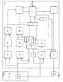
- the method of the invention for reducing a noise in a received signal is carried out in a contactless-card interrogator in which a transmitter-receiver module TRM; TRM' is connected both to an interrogator transmitter and an interrogator receiver ( Figs. 2 and 3 ).
- An interrogator local oscillator LO generates several output signals all having the same frequency; a first output signal is a carrier signal of a transmitter output signal.
- a receiver input signal is parallelly processed in two paths.
- a first receiver output signal is generated by combining the receiver input signal and a second output signal of the local oscillator LO, conducting the combined signal through a band-pass filter 321, where a direct-current component is eliminated and a portion of high-frequency noise components is strongly reduced, and amplifying it.
- a second receiver output signal is generated by combining the receiver input signal and a third output signal of the local oscillator LO being in quadrature to the second output signal of the local oscillator LO, conducting the combined signal through a band-pass filter 322 and amplifying it. The stronger of the first and the second receiver output signals is selected and digitized. The resulting signal is then conducted to a communication controller 1 which receives input signals and transmits output signals ios and communicates with a transmitter digital-to-analogue converter 2.
- the method of the invention for reducing the noise in the signal received in the contactless-card interrogator is characterized by the following steps.
- a calibrating output signal of the transmitter is generated in that the first output signal of the local oscillator LO is shallowly - in the order of magnitude of 1 % - amplitude-modulated with a pilot signal.
- the pilot signal frequency should equal the frequency at which the contactless-card encodes data.
- a receiver reference signal is generated in the interrogator by combining the calibrating output signal of the transmitter and a signal, whose carrier signal has a frequency equalling the frequency of the output signals of the local oscillator LO, conducting the combined signal through a band-pass filter 42 and amplifying it.
- the mentioned signal may be a fourth output signal of the local oscillator LO, whose phase is set in an appropriate way, so that its phase at an input of an auxiliary mixer stage 41 equals a phase of the calibrating output signal of the transmitter at the input of the auxiliary mixer stage 41 and a maximum effect of the amplitude demodulation is achieved; or the mentioned signal may simply be the calibrating output signal of the transmitter with a changed amplitude.
- the first and the second receiver output signals are cleared by subtracting the receiver reference signal, which has been attenuated by a calibrated factor and has been given a calibrated polarity of the first or the second receiver output signal, from the first and the second receiver output signal, respectively.
- the attenuation factor and the polarity of the receiver reference signal for each of both receiver output signals are sporadically recalibrated or whenever the conditions on the antenna or in the space around the antenna have substantially changed.
- the calibration of the attenuation factor of the receiver reference signal and its polarity for each of both receiver output signals is carried out in steps as contained in the following instruction.
- the attenuation factor of the receiver reference signal and its polarity for each one of both receiver output signals are determined and set as that pair of the calibrated values at which the first as well as the second cleared receiver output signal has the lowest amplitude.
- the method of the invention for reducing the noise in the signal received is carried out in the contactless-card interrogator, provided with the transmitter-receiver module TRM or TRM'.
- the transmitter-receiver module TRM comprises a coupling circuit CC and a transmitting and receiving antenna A ( Fig. 2 ).
- a directional coupler, a circulator or a discrete circuit provided for separating the received signal and the transmitter carrier signal may be used as the coupling circuit CC.
- the transmitter-receiver module TRM' comprises a transmitting antenna At, which is connected to the output of the interrogator transmitter, and a receiving antenna Ar, which is connected to the input of the interrogator receiver ( Fig. 3 ).
- a directional coupler e.g. attenuates the transmitter output signal in direction from the antenna towards the interrogator receiver much more strongly than the signal received from the contactless-card. A contribution of the noise from the transmitter output signal in the input signal of the interrogator receiver is thus reduced in this way by 20 dB to 30 dB, yet this contribution is still prevailing.
- the circuit of the invention for reducing the noise in the received signal is produced on a chip IC or IC' of the contactless-card interrogator.
- the transmitter-receiver module TRM or TRM' may be used on the chip IC or the chip IC' and is connected both to an output of a transmitter amplitude modulator 21, usually through a matching circuit MC, and to a first input of a first and a second receiver mixer stages 311,312.
- the first output signal of the local oscillator LO is conducted as the carrier signal of the transmitter output signal to a first input of the transmitter amplitude modulator 21. All output signals of the local oscillator LO have the same frequency.
- a modulation signal from a digital-to-analogue converter 2 is conducted to a second input of the transmitter amplitude modulator 21.
- the second and the third output signal of the local oscillator LO being in quadrature to each other are conducted to a second input of said first and second receiver mixer stage 311, 312, respectively.
- Output signals of said first and second receiver mixer stages 311, 312 are conducted through a first and a second band-pass filter and an amplifier 321, 322 to a first and a second input of a selection-digitalization circuit 3, respectively.
- Said selection-digitalization circuit 3 is connected to a communication controller 1.
- the circuit for reducing the noise in the signal received in the contactless-card interrogator is provided, as proposed by the invention, also with an auxiliary mixer stage 41, an auxiliary band-pass filter and an amplifier 42, a controlled first and a second circuit 4AP1, 4AP2 for attenuation and polarity setting, a first and a second subtractor 3S1, 3S2, a correction circuit 5 and a pilot-signal generator 6.
- the circuit of the invention is characterized by the following connections.
- the transmitter output signal which is tapped off in front of or behind the matching circuit MC or even behind the coupling circuit CC and may even be attenuated if necessary in order not to exceed the dynamic range of the input of the auxiliary mixer stage 41, is conducted to a first input of the auxiliary mixer stage 41.
- a signal is conducted whose carrier signal has a frequency of the output signal of the local oscillator LO.
- Said signal is either the fourth output signal of the local oscillator LO, which signal may be conducted through a phase shifter 40 to a second input of the auxiliary mixer stage 41, or the transmitter output signal which is supplied through a circuit 40' for setting the amplitude of the transmitter output signal.
- An output of the auxiliary mixer stage 41 is connected to the input of the circuit 42 representing the auxiliary band-pass filter and the amplifier.
- a demodulated transmitter output signal containing low-frequency components of the transmitter noise is present at an output of the circuit 42.
- a demodulated contactless-card signal is, strictly speaking, also present at the output of the circuit 42 representing the auxiliary band-pass filter and the amplifier, yet rather weak when compared to the demodulated low-frequency components of the transmitter noise.
- An output of the auxiliary band-pass filter and the amplifier circuit 42 is connected through the first and the second controlled attenuating and polarity setting circuit 4AP1, 4AP2 to a second input of the first and the second subtractors 3S1, 3S2, respectively.
- An output of the first and the second band-pass filter and amplifier 321, 322 is connected to a first input of the subtractor 3S1 and 3S2, respectively.
- an output of either subtractor 3S1 and 3S2 is connected to a first and a second input of the selection-digitalization circuit 3, respectively, and on the other hand to a first and a second input of the correction circuit 5, respectively.
- the correction circuit 5 controls the attenuating and polarity setting circuits 4AP1, 4AP2 in a manner that the first and the second receiver output signals, respectively, are optimally cleared also of low-frequency components of the demodulated amplitude noise of the transmitter output signal by means of the receiver reference signal from the output of the auxiliary band-pass filter and amplifier circuit 42 the receiver reference signal being scaled in an appropriate way described below.
- the correction circuit 5 controls the pilot-signal generator 6, as well.
- the pilot signal frequency equals the frequency, at which the contactless-card encodes data.
- An output of the pilot-signal generator 6 is connected to a second input of the interrogator transmitter amplitude modulator 21, said second input being provided for a modulating signal to be combined with the first output signal of the local oscillator LO.
- the transmitter amplitude modulator 21 is controlled by the communication controller 1.
- the correction circuit 5 When the correction circuit 5 has triggered the pilot signal generation, it also starts to observe the first and the second cleared receiver output signal and controls a setting of the attenuating and polarity setting circuits 4AP1, 4AP2, until it detects a minimum of the first and the second cleared receiver output signals.
- the circuit of the invention is thus calibrated.
- the correction circuit 5 freezes this setting and turns off the pilot-signal generator 6.
- the contactless-card interrogator is now prepared for an operation.
- the signal-to-noise ratio for the signal ios at the output of the communication controller 1 is significantly improved by the method and the circuit of the invention.
- the correction circuit 5 triggers the calibration action again.
Landscapes
- Engineering & Computer Science (AREA)
- Artificial Intelligence (AREA)
- Computer Vision & Pattern Recognition (AREA)
- Physics & Mathematics (AREA)
- General Physics & Mathematics (AREA)
- Theoretical Computer Science (AREA)
- Near-Field Transmission Systems (AREA)
Claims (18)
- Procédé pour réduire le bruit dans un signal reçu dans un interrogateur de carte sans contact dans lequel un module émetteur-récepteur est connecté à la fois à un émetteur d'interrogateur et à un récepteur d'interrogateur, et
un signal porteur d'un signal de sortie d'émetteur est un premier signal de sortie d'un oscillateur local, tous les signaux de sortie de l'oscillateur local ayant la même fréquence, et
un premier signal de sortie de récepteur est généré en combinant un signal d'entrée du récepteur et un deuxième signal de sortie de l'oscillateur local, en conduisant le signal combiné à travers un filtre passe-bande et en l'amplifiant, et
un deuxième signal de sortie de récepteur est généré en combinant le signal d'entrée du récepteur et un troisième signal de sortie de l'oscillateur local, en conduisant le signal combiné à travers un filtre passe-bande et en l'amplifiant, et
le signal le plus puissant desdits signaux de sortie du récepteur est sélectionné, numérisé et conduit vers un contrôleur de communication,
caractérisé
en ce qu'un signal de sortie d'étalonnage de l'émetteur est généré
de manière à ce que le premier signal de sortie de l'oscillateur local soit modulé en amplitudes peu profondes avec un signal pilote,
en ce qu'un signal de référence de récepteur scit généré
en combinant le signal de sortie d'étalonnage de l'émetteur et un signal,
dont le signal porteur a une fréquence égale à la fréquence des signaux de l'oscillateur local, en conduisant le signal combiné à travers un filtre passe-bande et en l'amplifiant,
en ce que les premier et deuxième signaux de sortie de récepteur sont nettoyés
en soustrayant le signal de référence du récepteur, lequel a été atténué par un facteur étalonné et a une polarité étalonnée,
depuis les premier et deuxième signaux de sortie du récepteur, respectivement,
et en ce que le facteur d'atténuation et la polarité du signal de référence du récepteur sont sporadiquement étalonnés pour chacun des deux signaux de sortie du récepteur
en déterminant et en définissant le facteur d'atténuation et la polarité du signal de référence du récepteur sous la forme d'une paire de valeurs pour chacun des deux signaux de sortie du récepteur, paire de valeurs, à laquelle les premier ainsi que deuxième signaux de sortie du récepteur nettoyés ont l'amplitude la plus faible. - Procédé tel que décrit dans la revendication 1, caractérisé
en ce que la fréquence du signal pilote est égale à la fréquence à laquelle la carte sans contact code les données. - Procédé tel que décrit dans la revendication 2, caractérisé
en ce que le facteur d'atténuation et la polarité du signal de référence du récepteur sont ré-étalonnés pour chacun des deux signaux de sortie du récepteur, à chaque fois que les conditions sur une antenne ou dans l'espace autour de l'antenne ont beaucoup changées. - Procédé tel que décrit dans la revendication 3, caractérisé
en ce que le signal de référence du récepteur est généré en combinant le signal de sortie de l'émetteur et un quatrième signal de sortie de l'oscillateur local. - Procédé tel que décrit dans la revendication 4, caractérisé
en ce que la phase du quatrième signal de sortie de l'oscillateur local est définie. - Procédé tel que décrit dans la revendication 3, caractérisé
en ce que le signal de référence du récepteur est généré en combinant le signal de sortie de l'émetteur et le même signal de sortie de l'émetteur avec une amplitude changée. - Procédé tel que décrit dans l'une quelconque des revendications 4, 5 ou 6, caractérisé
en ce que le module émetteur-récepteur comprend un circuit de couplage et l'antenne d'émission et de réception. - Procédé tel que décrit dans l'une quelconque des revendications 4, 5 ou 6, caractérisé
en ce que le module émetteur-récepteur comprend une antenne d'émission et l'antenne de réception. - Circuit pour réduire le bruit dans un signal reçu dans un interrogateur de carte sans contact,
dans lequel un module émetteur-récepteur (TRIM ; TRM') est connecté à la fois
à une sortie d'un modulateur d'amplitude (21) d'émetteur d'interrogateur
vers laquelle un premier signal de sortie d'un oscillateur local (LO), en tant que signal porteur d'un signal de sortie d'émetteur, est conduit
et à une première entrée d'un premier et d'un deuxième étages mélangeurs de récepteur (311, 312)
au niveau desquels un deuxième et un troisième signal de sortie de l'oscillateur local (LO) étant en quadrature l'un par rapport à l'autre sont conduits vers une deuxième entrée desdits premier et deuxième étages mélangeurs de récepteur (311, 312), respectivement, et
tous les signaux de sortie de l'oscillateur local (LO) ont la même fréquence, et
les signaux de sortie desdits premier et deuxième étages mélangeurs de récepteur (311, 312) sont conduits à travers des premier et deuxième filtres passe-bande et un amplificateur (321, 322), respectivement,
vers des première et deuxième entrées d'un circuit de numérisation de sélection (3), respectivement,
lequel circuit de numérisation de sélection (3) est connecté à un contrôleur de communication (1) qui est connecté à un convertisseur numérique-analogique (2),
dont la sortie est connectée à une première entrée du modulateur d'amplitude d'émetteur d'interrogateur (21) ladite première entrée étant pourvue pour qu'un signal de modulation soit combiné avec le premier signal de sortie de l'oscillateur local (LO),
caractérisé
en ce qu'un signal de sortie d'émetteur est conduit vers une première entrée d'un étage mélangeur auxiliaire (41)
vers la deuxième entrée duquel un signal est conduit, dont le signal porteur a une fréquence du signal de sortie de l'oscillateur local, et
dont la sortie est connectée à une entrée d'un filtre passe-bande auxiliaire et un amplificateur (42),
en ce qu'une sortie du filtre passe-bande auxiliaire et de l'amplificateur (42) est connectée
à travers des premier et deuxième circuits contrôlés d'atténuation et de fixation de la polarité (4AP1, 4AP2), à une deuxième entrée d'un premier et d'un deuxième soustracteurs (3S1, 3S2), respectivement,
vers la première entrée desquels une sortie des premier et deuxième filtres passe-bande et de l'amplificateur (321, 322), respectivement, est connectée, et
dont la sortie est connectée à la première et à la deuxième entrées du circuit de numérisation de sélection (3), respectivement,
en ce que les sorties des premier et deuxième soustracteurs (3S1, 3S2) sont connectées à une première et une deuxième entrées d'un circuit de correction (5), respectivement,
lequel contrôle les premier et deuxième circuits contrôlés d'atténuation et de fixation de la polarité (4AP1, 4AP2) et un générateur de signal pilote (6) dont la sortie est connectée à
une deuxième entrée du modulateur d'amplitude d'émetteur d'interrogateur (21), ladite deuxième entrée étant pourvue pour qu'un signal de modulation soit combiné avec le premier signal de sortie de l'oscillateur local (LO)
et en ce que le circuit de correction (5) est connecté au contrôleur de communication (1),
qui contrôle le modulateur d'amplitude d'émetteur d'interrogateur (21). - Circuit tel que décrit dans la revendication 9, caractérisé
en ce que la fréquence du signal pilote est égale à la fréquence à laquelle la carte sans contact code les données. - Circuit tel que décrit dans la revendication 10, caractérisé
en ce qu'un quatrième signal de sortie de l'oscillateur local (LO) est conduit vers la deuxième entrée de l'étage de mélangeur auxiliaire (41). - Circuit tel que décrit dans la revendication 11, caractérisé
en ce que le quatrième signal de sortie de l'oscillateur local (LO) est conduit à travers un déphaseur (40) vers la deuxième entrée de l'étage du mélangeur auxiliaire (41). - Circuit tel que décrit dans la revendication 10, caractérisé
en ce que le signal de sortie de l'émetteur est conduit à travers un circuit de définition d'amplitude de signal (40') vers la deuxième entrée de l'étage du mélangeur auxiliaire (41). - Circuit tel que décrit dans l'une quelconque des revendications 11, 12 ou 13, caractérisé
en ce que le module émetteur-récepteur (TRM) comprend un circuit de couplage (CC) et l'antenne de transmission et de réception (A). - Circuit tel que revendiqué dans la revendication 14, caractérisé
en ce que le circuit de couplage (CC) est un coupleur directionnel. - Circuit tel que revendiqué dans la revendication 14, caractérisé
en ce que le circuit de couplage (CC) est un circulateur. - Circuit tel que revendiqué dans la revendication 14, caractérisé
en ce que le circuit de couplage (CC) est un circuit discret pourvu pour séparer le signal reçu et le signal porteur de l'émetteur. - Circuit tel que revendiqué dans l'une quelconque des revendications 11, 12 ou 13, caractérisé
en ce que le module émetteur-récepteur (TRM') comprend une antenne de transmission (At) et une antenne de réception (Ar).
Applications Claiming Priority (1)
| Application Number | Priority Date | Filing Date | Title |
|---|---|---|---|
| PCT/SI2008/000025 WO2009128791A1 (fr) | 2008-04-15 | 2008-04-15 | Procédé pour réduire le bruit d'un signal reçu dans un interrogateur de carte sans contact, et circuit à cet effet |
Publications (3)
| Publication Number | Publication Date |
|---|---|
| EP2266072A1 EP2266072A1 (fr) | 2010-12-29 |
| EP2266072B1 true EP2266072B1 (fr) | 2013-02-13 |
| EP2266072B8 EP2266072B8 (fr) | 2013-04-17 |
Family
ID=39639650
Family Applications (1)
| Application Number | Title | Priority Date | Filing Date |
|---|---|---|---|
| EP08741975.0A Not-in-force EP2266072B8 (fr) | 2008-04-15 | 2008-04-15 | Procédé pour réduire le bruit d'un signal reçu dans un interrogateur de carte sans contact, et circuit à cet effet |
Country Status (4)
| Country | Link |
|---|---|
| US (1) | US8867989B2 (fr) |
| EP (1) | EP2266072B8 (fr) |
| CN (1) | CN102047268A (fr) |
| WO (1) | WO2009128791A1 (fr) |
Families Citing this family (4)
| Publication number | Priority date | Publication date | Assignee | Title |
|---|---|---|---|---|
| US8798198B2 (en) | 2011-08-31 | 2014-08-05 | Apple Inc. | Calibration systems for wireless electronic devices |
| SI23939A (sl) | 2011-11-30 | 2013-05-31 | Ids D.O.O. | Postopek za zmanjšanje amplitudnega šuma v sprejemanem signalu v RFID izpraševalniku |
| CN102902939B (zh) * | 2012-09-29 | 2015-07-22 | 中国物品编码中心 | 载波抵消装置 |
| GB2518254B (en) * | 2013-09-13 | 2020-12-16 | Vodafone Ip Licensing Ltd | Communicating with a machine to machine device |
Family Cites Families (3)
| Publication number | Priority date | Publication date | Assignee | Title |
|---|---|---|---|---|
| US7446806B2 (en) | 2003-12-19 | 2008-11-04 | Symbol Technologies, Inc. | Single chip, noise-resistant, one-dimensional, CMOS sensor for target imaging |
| US7583179B2 (en) * | 2005-02-22 | 2009-09-01 | Broadcom Corporation | Multi-protocol radio frequency identification transceiver |
| CN100392411C (zh) | 2005-10-11 | 2008-06-04 | 上海华虹集成电路有限责任公司 | 非接触智能卡噪声检测方法及其检测电路 |
-
2008
- 2008-04-15 US US12/736,504 patent/US8867989B2/en not_active Expired - Fee Related
- 2008-04-15 EP EP08741975.0A patent/EP2266072B8/fr not_active Not-in-force
- 2008-04-15 CN CN2008801295366A patent/CN102047268A/zh active Pending
- 2008-04-15 WO PCT/SI2008/000025 patent/WO2009128791A1/fr not_active Ceased
Also Published As
| Publication number | Publication date |
|---|---|
| EP2266072A1 (fr) | 2010-12-29 |
| EP2266072B8 (fr) | 2013-04-17 |
| CN102047268A (zh) | 2011-05-04 |
| US8867989B2 (en) | 2014-10-21 |
| US20110032080A1 (en) | 2011-02-10 |
| WO2009128791A1 (fr) | 2009-10-22 |
Similar Documents
| Publication | Publication Date | Title |
|---|---|---|
| KR100731227B1 (ko) | Rfid용 송수신 장치 | |
| EP1630713B1 (fr) | Procédé pour interrogateur par rétrodiffusion et interrogateur pour un système de rétrodiffusion modulé | |
| US7986931B2 (en) | RFID reader and circuit and method for echo cancellation thereof | |
| US7773545B2 (en) | Full division duplex system and a leakage cancellation method | |
| US8340214B2 (en) | Method and apparatus for generating predistortion signal | |
| TW200901644A (en) | Wireless receiver with notch filter to reduce effects of transmit signal leakage | |
| JP2011055457A (ja) | 送受信信号を分離するための結合装置及び制御方法 | |
| US7412217B2 (en) | Transceiver with interference signal rejection, and method for interference signal rejection | |
| CN109001693B (zh) | 调频连续波雷达直达波抑制的方法及系统 | |
| EP2266072B1 (fr) | Procédé pour réduire le bruit d'un signal reçu dans un interrogateur de carte sans contact, et circuit à cet effet | |
| CN112468221B (zh) | 一种用于微小卫星测传一体机的射频通道及测传一体机 | |
| JP4910586B2 (ja) | 送受信装置とこれを用いた電子機器 | |
| GB2414879A (en) | Radar receiver having an even harmonic mixer with an anti-parallel diode pair | |
| CN105049387B (zh) | 一种消除rfid系统后向链路载波干扰的方法 | |
| US6239656B1 (en) | Power amplifier | |
| CN120934555B (zh) | 全双工短距点对点毫米波通信系统及方法 | |
| JP4745054B2 (ja) | 無線受信装置及び無線通信装置 | |
| KR20020044946A (ko) | 이동통신 시스템의 기지국 수신장치 | |
| JP5200046B2 (ja) | 受信回路 | |
| JP2007074131A (ja) | 通信装置及び通信方法 | |
| JP2007142739A (ja) | 無線装置と高周波回路 | |
| JP2015216529A (ja) | 無線モジュール | |
| KR20020057263A (ko) | 이동통신 시스템의 적응 간섭 제어 장치 | |
| JPH11163829A (ja) | スペクトラム拡散通信装置 | |
| SI22435A (sl) | Postopek in vezje za zmanjšanje šuma v sprejetem signalu v izpraševalniku brezkontaktnih kartic |
Legal Events
| Date | Code | Title | Description |
|---|---|---|---|
| PUAI | Public reference made under article 153(3) epc to a published international application that has entered the european phase |
Free format text: ORIGINAL CODE: 0009012 |
|
| 17P | Request for examination filed |
Effective date: 20101104 |
|
| AK | Designated contracting states |
Kind code of ref document: A1 Designated state(s): AT BE BG CH CY CZ DE DK EE ES FI FR GB GR HR HU IE IS IT LI LT LU LV MC MT NL NO PL PT RO SE SI SK TR |
|
| AX | Request for extension of the european patent |
Extension state: AL BA MK RS |
|
| DAX | Request for extension of the european patent (deleted) | ||
| GRAP | Despatch of communication of intention to grant a patent |
Free format text: ORIGINAL CODE: EPIDOSNIGR1 |
|
| GRAS | Grant fee paid |
Free format text: ORIGINAL CODE: EPIDOSNIGR3 |
|
| GRAA | (expected) grant |
Free format text: ORIGINAL CODE: 0009210 |
|
| AK | Designated contracting states |
Kind code of ref document: B1 Designated state(s): AT BE BG CH CY CZ DE DK EE ES FI FR GB GR HR HU IE IS IT LI LT LU LV MC MT NL NO PL PT RO SE SI SK TR |
|
| REG | Reference to a national code |
Ref country code: GB Ref legal event code: FG4D |
|
| REG | Reference to a national code |
Ref country code: AT Ref legal event code: REF Ref document number: 596824 Country of ref document: AT Kind code of ref document: T Effective date: 20130215 |
|
| RAP2 | Party data changed (patent owner data changed or rights of a patent transferred) |
Owner name: ATANASIJEVIC-KUNC, MAJA Owner name: VODOPIVEC, ANDREJ Owner name: IDS MICROCHIP AG Owner name: STERN, ANTON |
|
| RIN2 | Information on inventor provided after grant (corrected) |
Inventor name: KUNC, VINKO Inventor name: ATANASIJEVIC-KUNC, MAJA Inventor name: VODOPIVEC, ANDREJ Inventor name: STERN, ANTON |
|
| REG | Reference to a national code |
Ref country code: IE Ref legal event code: FG4D |
|
| RAP2 | Party data changed (patent owner data changed or rights of a patent transferred) |
Owner name: IDS MICROCHIP AG |
|
| REG | Reference to a national code |
Ref country code: DE Ref legal event code: R096 Ref document number: 602008022107 Country of ref document: DE Effective date: 20130411 |
|
| PGFP | Annual fee paid to national office [announced via postgrant information from national office to epo] |
Ref country code: CH Payment date: 20130322 Year of fee payment: 6 |
|
| REG | Reference to a national code |
Ref country code: DE Ref legal event code: R081 Ref document number: 602008022107 Country of ref document: DE Owner name: IDS MICROCHIP AG, CH Free format text: FORMER OWNER: MAJA ATANASIJEVIC-KUNC, IDS MICROCHIP AG,ANTON STERN,ANDREJ VODOPIVEC, , SI Effective date: 20130507 Ref country code: DE Ref legal event code: R081 Ref document number: 602008022107 Country of ref document: DE Owner name: IDS MICROCHIP AG, CH Free format text: FORMER OWNERS: ATANASIJEVIC-KUNC, MAJA, LJUBLJANA, SI; IDS MICROCHIP AG, WOLLERAU, CH; STERN, ANTON, PREDDVOR, SI; VODOPIVEC, ANDREJ, LJUBLJANA, SI Effective date: 20130507 Ref country code: DE Ref legal event code: R081 Ref document number: 602008022107 Country of ref document: DE Owner name: AMS INTERNATIONAL AG, CH Free format text: FORMER OWNERS: ATANASIJEVIC-KUNC, MAJA, LJUBLJANA, SI; IDS MICROCHIP AG, WOLLERAU, CH; STERN, ANTON, PREDDVOR, SI; VODOPIVEC, ANDREJ, LJUBLJANA, SI Effective date: 20130507 Ref country code: DE Ref legal event code: R081 Ref document number: 602008022107 Country of ref document: DE Owner name: STMICROEELECTRONICS INTERNATIONAL N.V., NL Free format text: FORMER OWNERS: ATANASIJEVIC-KUNC, MAJA, LJUBLJANA, SI; IDS MICROCHIP AG, WOLLERAU, CH; STERN, ANTON, PREDDVOR, SI; VODOPIVEC, ANDREJ, LJUBLJANA, SI Effective date: 20130507 Ref country code: DE Ref legal event code: R081 Ref document number: 602008022107 Country of ref document: DE Owner name: STMICROELECTROLONICS INTERNATIONAL N.V., NL Free format text: FORMER OWNERS: ATANASIJEVIC-KUNC, MAJA, LJUBLJANA, SI; IDS MICROCHIP AG, WOLLERAU, CH; STERN, ANTON, PREDDVOR, SI; VODOPIVEC, ANDREJ, LJUBLJANA, SI Effective date: 20130507 Ref country code: DE Ref legal event code: R081 Ref document number: 602008022107 Country of ref document: DE Owner name: STMICROELECTRONICS INTERNATIONAL N.V., NL Free format text: FORMER OWNERS: ATANASIJEVIC-KUNC, MAJA, LJUBLJANA, SI; IDS MICROCHIP AG, WOLLERAU, CH; STERN, ANTON, PREDDVOR, SI; VODOPIVEC, ANDREJ, LJUBLJANA, SI Effective date: 20130507 |
|
| REG | Reference to a national code |
Ref country code: AT Ref legal event code: MK05 Ref document number: 596824 Country of ref document: AT Kind code of ref document: T Effective date: 20130213 |
|
| REG | Reference to a national code |
Ref country code: NL Ref legal event code: VDEP Effective date: 20130213 |
|
| REG | Reference to a national code |
Ref country code: LT Ref legal event code: MG4D |
|
| PG25 | Lapsed in a contracting state [announced via postgrant information from national office to epo] |
Ref country code: LT Free format text: LAPSE BECAUSE OF FAILURE TO SUBMIT A TRANSLATION OF THE DESCRIPTION OR TO PAY THE FEE WITHIN THE PRESCRIBED TIME-LIMIT Effective date: 20130213 Ref country code: AT Free format text: LAPSE BECAUSE OF FAILURE TO SUBMIT A TRANSLATION OF THE DESCRIPTION OR TO PAY THE FEE WITHIN THE PRESCRIBED TIME-LIMIT Effective date: 20130213 Ref country code: SE Free format text: LAPSE BECAUSE OF FAILURE TO SUBMIT A TRANSLATION OF THE DESCRIPTION OR TO PAY THE FEE WITHIN THE PRESCRIBED TIME-LIMIT Effective date: 20130213 Ref country code: NO Free format text: LAPSE BECAUSE OF FAILURE TO SUBMIT A TRANSLATION OF THE DESCRIPTION OR TO PAY THE FEE WITHIN THE PRESCRIBED TIME-LIMIT Effective date: 20130513 Ref country code: IS Free format text: LAPSE BECAUSE OF FAILURE TO SUBMIT A TRANSLATION OF THE DESCRIPTION OR TO PAY THE FEE WITHIN THE PRESCRIBED TIME-LIMIT Effective date: 20130613 Ref country code: ES Free format text: LAPSE BECAUSE OF FAILURE TO SUBMIT A TRANSLATION OF THE DESCRIPTION OR TO PAY THE FEE WITHIN THE PRESCRIBED TIME-LIMIT Effective date: 20130524 Ref country code: BG Free format text: LAPSE BECAUSE OF FAILURE TO SUBMIT A TRANSLATION OF THE DESCRIPTION OR TO PAY THE FEE WITHIN THE PRESCRIBED TIME-LIMIT Effective date: 20130513 |
|
| PGFP | Annual fee paid to national office [announced via postgrant information from national office to epo] |
Ref country code: GB Payment date: 20130422 Year of fee payment: 6 |
|
| PG25 | Lapsed in a contracting state [announced via postgrant information from national office to epo] |
Ref country code: SI Free format text: LAPSE BECAUSE OF FAILURE TO SUBMIT A TRANSLATION OF THE DESCRIPTION OR TO PAY THE FEE WITHIN THE PRESCRIBED TIME-LIMIT Effective date: 20130213 Ref country code: PT Free format text: LAPSE BECAUSE OF FAILURE TO SUBMIT A TRANSLATION OF THE DESCRIPTION OR TO PAY THE FEE WITHIN THE PRESCRIBED TIME-LIMIT Effective date: 20130613 Ref country code: GR Free format text: LAPSE BECAUSE OF FAILURE TO SUBMIT A TRANSLATION OF THE DESCRIPTION OR TO PAY THE FEE WITHIN THE PRESCRIBED TIME-LIMIT Effective date: 20130514 Ref country code: PL Free format text: LAPSE BECAUSE OF FAILURE TO SUBMIT A TRANSLATION OF THE DESCRIPTION OR TO PAY THE FEE WITHIN THE PRESCRIBED TIME-LIMIT Effective date: 20130213 Ref country code: BE Free format text: LAPSE BECAUSE OF FAILURE TO SUBMIT A TRANSLATION OF THE DESCRIPTION OR TO PAY THE FEE WITHIN THE PRESCRIBED TIME-LIMIT Effective date: 20130213 Ref country code: LV Free format text: LAPSE BECAUSE OF FAILURE TO SUBMIT A TRANSLATION OF THE DESCRIPTION OR TO PAY THE FEE WITHIN THE PRESCRIBED TIME-LIMIT Effective date: 20130213 Ref country code: FI Free format text: LAPSE BECAUSE OF FAILURE TO SUBMIT A TRANSLATION OF THE DESCRIPTION OR TO PAY THE FEE WITHIN THE PRESCRIBED TIME-LIMIT Effective date: 20130213 |
|
| PGFP | Annual fee paid to national office [announced via postgrant information from national office to epo] |
Ref country code: FR Payment date: 20130618 Year of fee payment: 6 |
|
| PG25 | Lapsed in a contracting state [announced via postgrant information from national office to epo] |
Ref country code: HR Free format text: LAPSE BECAUSE OF FAILURE TO SUBMIT A TRANSLATION OF THE DESCRIPTION OR TO PAY THE FEE WITHIN THE PRESCRIBED TIME-LIMIT Effective date: 20130213 |
|
| PG25 | Lapsed in a contracting state [announced via postgrant information from national office to epo] |
Ref country code: NL Free format text: LAPSE BECAUSE OF FAILURE TO SUBMIT A TRANSLATION OF THE DESCRIPTION OR TO PAY THE FEE WITHIN THE PRESCRIBED TIME-LIMIT Effective date: 20130213 Ref country code: SK Free format text: LAPSE BECAUSE OF FAILURE TO SUBMIT A TRANSLATION OF THE DESCRIPTION OR TO PAY THE FEE WITHIN THE PRESCRIBED TIME-LIMIT Effective date: 20130213 Ref country code: CZ Free format text: LAPSE BECAUSE OF FAILURE TO SUBMIT A TRANSLATION OF THE DESCRIPTION OR TO PAY THE FEE WITHIN THE PRESCRIBED TIME-LIMIT Effective date: 20130213 Ref country code: DK Free format text: LAPSE BECAUSE OF FAILURE TO SUBMIT A TRANSLATION OF THE DESCRIPTION OR TO PAY THE FEE WITHIN THE PRESCRIBED TIME-LIMIT Effective date: 20130213 Ref country code: RO Free format text: LAPSE BECAUSE OF FAILURE TO SUBMIT A TRANSLATION OF THE DESCRIPTION OR TO PAY THE FEE WITHIN THE PRESCRIBED TIME-LIMIT Effective date: 20130213 Ref country code: EE Free format text: LAPSE BECAUSE OF FAILURE TO SUBMIT A TRANSLATION OF THE DESCRIPTION OR TO PAY THE FEE WITHIN THE PRESCRIBED TIME-LIMIT Effective date: 20130213 |
|
| PG25 | Lapsed in a contracting state [announced via postgrant information from national office to epo] |
Ref country code: MC Free format text: LAPSE BECAUSE OF FAILURE TO SUBMIT A TRANSLATION OF THE DESCRIPTION OR TO PAY THE FEE WITHIN THE PRESCRIBED TIME-LIMIT Effective date: 20130213 |
|
| PLBE | No opposition filed within time limit |
Free format text: ORIGINAL CODE: 0009261 |
|
| STAA | Information on the status of an ep patent application or granted ep patent |
Free format text: STATUS: NO OPPOSITION FILED WITHIN TIME LIMIT |
|
| PG25 | Lapsed in a contracting state [announced via postgrant information from national office to epo] |
Ref country code: IT Free format text: LAPSE BECAUSE OF FAILURE TO SUBMIT A TRANSLATION OF THE DESCRIPTION OR TO PAY THE FEE WITHIN THE PRESCRIBED TIME-LIMIT Effective date: 20130213 |
|
| 26N | No opposition filed |
Effective date: 20131114 |
|
| REG | Reference to a national code |
Ref country code: IE Ref legal event code: MM4A |
|
| REG | Reference to a national code |
Ref country code: DE Ref legal event code: R097 Ref document number: 602008022107 Country of ref document: DE Effective date: 20131114 |
|
| PG25 | Lapsed in a contracting state [announced via postgrant information from national office to epo] |
Ref country code: IE Free format text: LAPSE BECAUSE OF NON-PAYMENT OF DUE FEES Effective date: 20130415 |
|
| REG | Reference to a national code |
Ref country code: CH Ref legal event code: PL |
|
| GBPC | Gb: european patent ceased through non-payment of renewal fee |
Effective date: 20140415 |
|
| REG | Reference to a national code |
Ref country code: FR Ref legal event code: ST Effective date: 20141231 |
|
| PG25 | Lapsed in a contracting state [announced via postgrant information from national office to epo] |
Ref country code: GB Free format text: LAPSE BECAUSE OF NON-PAYMENT OF DUE FEES Effective date: 20140415 Ref country code: LI Free format text: LAPSE BECAUSE OF NON-PAYMENT OF DUE FEES Effective date: 20140430 Ref country code: CH Free format text: LAPSE BECAUSE OF NON-PAYMENT OF DUE FEES Effective date: 20140430 |
|
| PG25 | Lapsed in a contracting state [announced via postgrant information from national office to epo] |
Ref country code: MT Free format text: LAPSE BECAUSE OF FAILURE TO SUBMIT A TRANSLATION OF THE DESCRIPTION OR TO PAY THE FEE WITHIN THE PRESCRIBED TIME-LIMIT Effective date: 20130213 Ref country code: FR Free format text: LAPSE BECAUSE OF NON-PAYMENT OF DUE FEES Effective date: 20140430 |
|
| PG25 | Lapsed in a contracting state [announced via postgrant information from national office to epo] |
Ref country code: TR Free format text: LAPSE BECAUSE OF FAILURE TO SUBMIT A TRANSLATION OF THE DESCRIPTION OR TO PAY THE FEE WITHIN THE PRESCRIBED TIME-LIMIT Effective date: 20130213 Ref country code: CY Free format text: LAPSE BECAUSE OF FAILURE TO SUBMIT A TRANSLATION OF THE DESCRIPTION OR TO PAY THE FEE WITHIN THE PRESCRIBED TIME-LIMIT Effective date: 20130213 |
|
| PG25 | Lapsed in a contracting state [announced via postgrant information from national office to epo] |
Ref country code: HU Free format text: LAPSE BECAUSE OF FAILURE TO SUBMIT A TRANSLATION OF THE DESCRIPTION OR TO PAY THE FEE WITHIN THE PRESCRIBED TIME-LIMIT; INVALID AB INITIO Effective date: 20080415 Ref country code: LU Free format text: LAPSE BECAUSE OF NON-PAYMENT OF DUE FEES Effective date: 20130415 |
|
| REG | Reference to a national code |
Ref country code: DE Ref legal event code: R082 Ref document number: 602008022107 Country of ref document: DE Representative=s name: EPPING HERMANN FISCHER, PATENTANWALTSGESELLSCH, DE Ref country code: DE Ref legal event code: R081 Ref document number: 602008022107 Country of ref document: DE Owner name: AMS INTERNATIONAL AG, CH Free format text: FORMER OWNER: IDS MICROCHIP AG, WOLLERAU, CH Ref country code: DE Ref legal event code: R081 Ref document number: 602008022107 Country of ref document: DE Owner name: STMICROEELECTRONICS INTERNATIONAL N.V., NL Free format text: FORMER OWNER: IDS MICROCHIP AG, WOLLERAU, CH Ref country code: DE Ref legal event code: R082 Ref document number: 602008022107 Country of ref document: DE Representative=s name: CASALONGA & PARTNERS, DE Ref country code: DE Ref legal event code: R081 Ref document number: 602008022107 Country of ref document: DE Owner name: STMICROELECTROLONICS INTERNATIONAL N.V., NL Free format text: FORMER OWNER: IDS MICROCHIP AG, WOLLERAU, CH Ref country code: DE Ref legal event code: R081 Ref document number: 602008022107 Country of ref document: DE Owner name: STMICROELECTRONICS INTERNATIONAL N.V., NL Free format text: FORMER OWNER: IDS MICROCHIP AG, WOLLERAU, CH |
|
| REG | Reference to a national code |
Ref country code: DE Ref legal event code: R082 Ref document number: 602008022107 Country of ref document: DE Representative=s name: CASALONGA & PARTNERS, DE Ref country code: DE Ref legal event code: R081 Ref document number: 602008022107 Country of ref document: DE Owner name: STMICROEELECTRONICS INTERNATIONAL N.V., NL Free format text: FORMER OWNER: AMS INTERNATIONAL AG, RAPPERSWIL, CH Ref country code: DE Ref legal event code: R081 Ref document number: 602008022107 Country of ref document: DE Owner name: STMICROELECTROLONICS INTERNATIONAL N.V., NL Free format text: FORMER OWNER: AMS INTERNATIONAL AG, RAPPERSWIL, CH Ref country code: DE Ref legal event code: R081 Ref document number: 602008022107 Country of ref document: DE Owner name: STMICROELECTRONICS INTERNATIONAL N.V., NL Free format text: FORMER OWNER: AMS INTERNATIONAL AG, RAPPERSWIL, CH |
|
| REG | Reference to a national code |
Ref country code: DE Ref legal event code: R081 Ref document number: 602008022107 Country of ref document: DE Owner name: STMICROELECTRONICS INTERNATIONAL N.V., NL Free format text: FORMER OWNER: STMICROEELECTRONICS INTERNATIONAL N.V., SCHIPOL, NL Ref country code: DE Ref legal event code: R082 Ref document number: 602008022107 Country of ref document: DE Representative=s name: CASALONGA & PARTNERS, DE |
|
| REG | Reference to a national code |
Ref country code: DE Ref legal event code: R081 Ref document number: 602008022107 Country of ref document: DE Owner name: STMICROELECTRONICS INTERNATIONAL N.V., NL Free format text: FORMER OWNER: STMICROELECTRONICS INTERNATIONAL N.V., SCHIPHOL, NL Ref country code: DE Ref legal event code: R082 Ref document number: 602008022107 Country of ref document: DE Representative=s name: CASALONGA & PARTNERS, DE |
|
| PGFP | Annual fee paid to national office [announced via postgrant information from national office to epo] |
Ref country code: DE Payment date: 20210323 Year of fee payment: 14 |
|
| REG | Reference to a national code |
Ref country code: DE Ref legal event code: R119 Ref document number: 602008022107 Country of ref document: DE |
|
| PG25 | Lapsed in a contracting state [announced via postgrant information from national office to epo] |
Ref country code: DE Free format text: LAPSE BECAUSE OF NON-PAYMENT OF DUE FEES Effective date: 20221103 |