EP2267768A2 - Stütze für vertikal ausgerichtete Kondensatoren während der Herstellung einer Halbleitervorrichtung - Google Patents
Stütze für vertikal ausgerichtete Kondensatoren während der Herstellung einer Halbleitervorrichtung Download PDFInfo
- Publication number
- EP2267768A2 EP2267768A2 EP10010273A EP10010273A EP2267768A2 EP 2267768 A2 EP2267768 A2 EP 2267768A2 EP 10010273 A EP10010273 A EP 10010273A EP 10010273 A EP10010273 A EP 10010273A EP 2267768 A2 EP2267768 A2 EP 2267768A2
- Authority
- EP
- European Patent Office
- Prior art keywords
- layer
- capacitor
- dielectric layer
- electrode
- etch
- Prior art date
- Legal status (The legal status is an assumption and is not a legal conclusion. Google has not performed a legal analysis and makes no representation as to the accuracy of the status listed.)
- Withdrawn
Links
Images










Classifications
-
- H—ELECTRICITY
- H10—SEMICONDUCTOR DEVICES; ELECTRIC SOLID-STATE DEVICES NOT OTHERWISE PROVIDED FOR
- H10D—INORGANIC ELECTRIC SEMICONDUCTOR DEVICES
- H10D1/00—Resistors, capacitors or inductors
- H10D1/01—Manufacture or treatment
- H10D1/041—Manufacture or treatment of capacitors having no potential barriers
- H10D1/042—Manufacture or treatment of capacitors having no potential barriers using deposition processes to form electrode extensions
-
- H—ELECTRICITY
- H10—SEMICONDUCTOR DEVICES; ELECTRIC SOLID-STATE DEVICES NOT OTHERWISE PROVIDED FOR
- H10B—ELECTRONIC MEMORY DEVICES
- H10B12/00—Dynamic random access memory [DRAM] devices
- H10B12/01—Manufacture or treatment
- H10B12/02—Manufacture or treatment for one transistor one-capacitor [1T-1C] memory cells
- H10B12/03—Making the capacitor or connections thereto
- H10B12/033—Making the capacitor or connections thereto the capacitor extending over the transistor
-
- H—ELECTRICITY
- H10—SEMICONDUCTOR DEVICES; ELECTRIC SOLID-STATE DEVICES NOT OTHERWISE PROVIDED FOR
- H10B—ELECTRONIC MEMORY DEVICES
- H10B12/00—Dynamic random access memory [DRAM] devices
- H10B12/01—Manufacture or treatment
- H10B12/09—Manufacture or treatment with simultaneous manufacture of the peripheral circuit region and memory cells
-
- H—ELECTRICITY
- H10—SEMICONDUCTOR DEVICES; ELECTRIC SOLID-STATE DEVICES NOT OTHERWISE PROVIDED FOR
- H10B—ELECTRONIC MEMORY DEVICES
- H10B12/00—Dynamic random access memory [DRAM] devices
- H10B12/30—DRAM devices comprising one-transistor - one-capacitor [1T-1C] memory cells
- H10B12/31—DRAM devices comprising one-transistor - one-capacitor [1T-1C] memory cells having a storage electrode stacked over the transistor
- H10B12/318—DRAM devices comprising one-transistor - one-capacitor [1T-1C] memory cells having a storage electrode stacked over the transistor the storage electrode having multiple segments
-
- H—ELECTRICITY
- H10—SEMICONDUCTOR DEVICES; ELECTRIC SOLID-STATE DEVICES NOT OTHERWISE PROVIDED FOR
- H10D—INORGANIC ELECTRIC SEMICONDUCTOR DEVICES
- H10D1/00—Resistors, capacitors or inductors
- H10D1/60—Capacitors
- H10D1/68—Capacitors having no potential barriers
- H10D1/692—Electrodes
- H10D1/711—Electrodes having non-planar surfaces, e.g. formed by texturisation
- H10D1/716—Electrodes having non-planar surfaces, e.g. formed by texturisation having vertical extensions
Definitions
- This invention relates to the field of semiconductor devices and manufacture thereof and, more particularly, to capacitor devices having lateral support for their capacitor bottom plates.
- capacitors such as container capacitors and pedestal capacitors are commonly formed.
- Container and pedestal capacitors are well known to allow an increased stored charge over planar capacitors by increasing the surface on which the charge may be stored.
- FIGS. 1-7 depict a conventional method for forming a plurality of container capacitors from polysilicon. Formation of a pedestal capacitor is similar, but the bottom plate is a solid plug and the cell dielectric and top plate are conformal with the exterior of the bottom plate to form a single-sided vertically-oriented capacitor.
- FIG. 1 depicts a semiconductor wafer substrate assembly 10 comprising a semiconductor wafer 12 having a plurality of doped source/drain regions 14 within the wafer 12.
- FIG. 1 further depicts transistors 16 comprising gate oxide 18, a doped polysilicon control gate 20, silicide 22 such as tungsten silicide which increases conductivity of the control gate 20, and a capping layer 24 often manufactured from silicon nitride.
- Silicon nitride spacers 26 are formed to insulate the control gate 20 and silicde 22 from polysilicon pads 28 to which the container capacitors will be electrically coupled. Shallow trench isolation (STI, field oxide) 30 reduces unwanted electrical interaction between adjacent control gates.
- An etch stop layer 31 is formed, then a thick layer of deposited oxide 32 such as borophosphosilicate glass (BPSG) formed to provide a base dielectric layer for capacitor features which are formed later.
- BPSG borophosphosilicate glass
- a patterned photoresist layer 34 defines the location of the container capacitors to be formed.
- the FIG. 1 structure may further include one or more bit (digit) lines under the BPSG layer or various other structural elements or differences which, for simplicity of explanation, have not been depicted.
- the FIG. 1 structure is subjected to an anisotropic etch which removes the exposed portions of the BPSG layer to expose the etch stop layer 31 and to form a patterned BPSG layer which provides a base dielectric having recesses for the capacitors.
- the exposed portion of the etch stop is the removed.
- the polysilicon pads 28 and possibly a portion of capping layer 24 are exposed to result in a structure similar to FIG. 2 .
- the remaining photoresist layer 34 is stripped and any polymer (not depicted) which forms during the etch is removed according to means known in the art to provide the FIG. 3 structure.
- a blanket conductive layer 40 such as polysilicon or another material is formed conformal with the deposited oxide layer, and will provide a capacitor storage node for the completed capacitor.
- a thick blanket filler material 42 such as photoresist, is formed to fill the containers provided by polysilicon 40.
- the FIG. 4 structure is then subjected to a planarizing process, such as a chemical planarization, a mechanical planarization, or a chemical mechanical planarization (CMP) step. This process removes portions of the photoresist 42, the polysilicon 40, and usually a portion of the BPSG 32 to result in the FIG. 5 structure.
- CMP chemical mechanical planarization
- the BPSG 32 is partially etched with an etch selective to polysilicon (i.e. an etch which minimally etches or, preferably, doesn't etch polysilicon) to result in the structure of FIG. 6 .
- the polysilicon storage nodes (capacitor bottom plates) 40 are only minimally supported.
- the bottom plates 40 in the FIG. 6 structure each comprise a first region 60 which defines a recess, and a second region 62 which defines an opening to the recess, with the first and second regions being continuous, each with the other.
- the bottom plate 40 of FIG. 6 defines a receptacle having a rim 62 which defines an opening to the interior of the receptacle.
- the regions 60, 62 form vertically-oriented sides of the bottom plate, and the sides are electrically-coupled by a horizontally-oriented bottom 64.
- a cell dielectric layer 70 for example a layer of high-quality cell nitride, a polysilicon container capacitor top plate 72, and a planar oxide layer such as BPSG 74 are formed according to means known in the art to result in the FIG. 7 structure.
- wafer processing continues according to means known in the art.
- FIG. 6 It can be seen at the FIG. 6 structure that conventional processes remove the oxide 32 which supports the capacitor bottom plate 40. This oxide removal is performed to allow formation of the cell dielectric and capacitor top plate on both sides of the bottom plate to form a double-sided capacitor.
- the structure of FIG. 6 is easily damaged and susceptible to defects such as leaning (caused, for example, during the etch of BPSG 32 of FIG. 5 to result in FIG. 6 ), toppling, or lifting of the bottom plate.
- leaning caused, for example, during the etch of BPSG 32 of FIG. 5 to result in FIG. 6
- etch tool technology can etch contacts to a depth of about 3.0 micrometers ( ⁇ m) to about 3.5 ⁇ m. If the capacitor height causes the contact depth to go beyond the 3.0 ⁇ m to 3.5 ⁇ m limit, then additional masking layers will be needed. One way to do this is to form a portion of the contact to diffusion areas in the wafer before forming the capacitor, then forming the remaining portion after forming the capacitor. Such a process is complex and adds significantly to device cost.
- BPSG layer 32 of FIG. 5 Another problem which can occur during conventional processing results indirectly from the etch of BPSG layer 32 of FIG. 5 to result in the FIG. 6 structure.
- BPSG over the device periphery (not depicted) is also etched, which forms a step in the oxide between the periphery, where there are no cell capacitors, and the array, where the tops of the cell capacitors are at the original level of the top of BPSG 32.
- the periphery region After forming the cell dielectric and top plate, the periphery region must be backfilled with oxide, which is then planarized. The requirement to backfill planarize results in additional processing steps, which contributes to a further increase in costs.
- a method used to form a double-sided capacitor such as a container capacitor or a pedestal capacitor which reduces or eliminates one or more the problems described above, and a structure resulting therefrom, would be desirable.
- Embodiments of the present invention provide devices which, among other advantages, reduce problems associated with the manufacture of semiconductor devices, particularly problems resulting from instability of unsupported capacitor bottom plates prior to formation of a supporting layer.
- Various embodiments of the present invention provide lateral support for a vertically-oriented structure, for example a storage capacitor such as a container capacitor or a pedestal capacitor.
- a storage capacitor such as a container capacitor or a pedestal capacitor.
- a method for forming a semiconductor device comprising forming a plurality of container capacitor bottom plates within a base dielectric layer; forming a supporting collar around each of the capacitor bottom plates, the supporting collar having a plurality of openings therein which expose the base dielectric layer and etching the base dielectric layer through the openings in the collar to expose sidewalls of the plurality of container capacitor bottom plates, wherein subsequent to etching the base dielectric layer the supporting collar supports each of the plurality of container capacitor bottom plates.
- the method may further comprise forming a cell dielectric on the sidewalls of the plurality of container capacitor bottom plates and on the supporting collar, and may further comprise forming a capacitor top plate on the cell dielectric layer and over the supporting collar.
- the method may further comprise removing substantially all of the base dielectric layer during the etching of the base dielectric layer through the openings in the collar such that the collar contacts the plurality capacitor bottom plates and is generally free from contact with any other layer.
- the method may further comprise forming a blanket layer from a material selected from the group consisting of silicon dioxide, borophosphosilicate glass, and tetraethyl orthosilicate on a horizontal surface of the base dielectric layer; and etching the blanket layer to form the supporting collar.
- the method may further comprise forming a blanket supporting collar layer prior to forming the container capacitor bottom plates; etching the base dielectric layer and the blanket collar layer to form a plurality of openings therein; forming one of the plurality of container capacitor bottom plates within each opening in the base dielectric layer and in the blanket collar layer; only partially etching the collar layer to expose an upper sidewall of each container capacitor bottom plate and subsequent to only partially etching the collar layer to expose the upper sidewall of each container capacitor bottom plate, performing the etch of the base dielectric layer through the openings in the collar.
- the method may further comprise forming a blanket supporting collar layer prior to forming the container capacitor bottom plates; forming a blanket sacrificial layer on the blanket collar layer; etching the blanket sacrificial layer, the blanket collar layer, and the base dielectric layer to form a plurality of openings therein; forming one of the plurality of container capacitor bottom plates within each opening in the blanket sacrificial layer, in the blanket collar layer, and in the base dielectric layer; etching the sacrificial layer to expose an upper sidewall of each container capacitor bottom plate and to expose the collar layer and subsequent to etching the sacrificial layer, performing the etch of the base dielectric layer through the openings in the collar.
- the method may further comprise prior to forming the plurality of container capacitor bottom plates with the base dielectric layer, etching the base dielectric layer to form a plurality of openings therein which define container capacitor bottom plates, and a plurality of openings therein which define a plurality of moats, with one moat around each array of a semiconductor die; forming a container capacitor bottom plate layer in the plurality of openings which define container capacitor bottom plates and in the openings which define the plurality of moats and during the etch of the base dielectric layer through the openings in the collar, using the container capacitor bottom plate layer in the openings which define the plurality of moats as an etch stop to protect a periphery of the semiconductor die.
- a method used to form a semiconductor device comprising forming a patterned base dielectric layer over a semiconductor wafer substrate assembly; forming a support layer over the patterned base dielectric layer; forming a sacrificial layer over the support layer; removing a portion of the sacrificial layer, the support layer, and the patterned base dielectric layer to form a recess defined by the sacrificial layer, the support layer, and the patterned base dielectric layer; forming a capacitor bottom plate within the recess, the bottom plate contacting the sacrificial layer, the support layer, and the patterned base dielectric layer; subsequent to forming the capacitor bottom plate, removing the sacrificial layer to leave a portion of the bottom plate protruding from the support layer; forming masking spacers along the protruding portion of the bottom plate; etching the support layer using the masking spacers as a mask to form openings in the support layer and etching the base dielectric layer through the
- the method further comprising forming at least first, second, and third capacitor bottom plates such that, in cross section, a first distance between the first and second capacitor bottom plates is greater than a second distance between the second and third capacitor bottom plates; removing the sacrificial layer to leave a portion of the first, second and third bottom plates protruding from the support layer; forming a masking spacer layer between the first and second capacitor bottom plate and between the second and third capacitor bottom plate such that the masking spacer layer bridges between the first and second capacitor bottom plates and bridges between the second and third capacitor bottom plates; and performing an anisotropic etch on the masking spacer layer to form the masking spacers along the protruding portions of the bottom plates, such that, subsequent to the anisotropic etch, the masking spacer layer, in the cross section, does not bridge between first and second capacitor bottom plates and bridges between the second and third capacitor bottom plates.
- the method may further comprise forming the capacitor bottom plate conformal with the recess defined by the sacrificial layer, the support layer, and the patterned base dielectric later such that the capacitor bottom plate has a recess therein.
- the method may further comprise forming a capacitor bottom plate layer to completely fill the recess defined by the sacrificial layer, the support layer, and the patterned base dielectric layer and to overlie a horizontal surface of the sacrificial layer and planarizing the capacitor bottom plate and the sacrificial layer to remove the capacitor bottom plate layer from the horizontal surface of the sacrificial layer and to form the capacitor bottom plate.
- an in-process semiconductor device comprising a plurality of container capacitor bottom plates, with each plate comprising a bottom and first and second cross-sectional, vertically-oriented sides each having a height, , with each side being unsupported along a majority of its height; a supporting layer having a bottom surface and a top surface, wherein the supporting layer contacts each container capacitor bottom plate of the plurality of bottom plates, and wherein the top and bottom surfaces of the supporting layer is generally free from contact with any other layer.
- the supporting layer may be a material selected from the group consisting of silicon dioxide, borophosphosilicate glass, and tetraethyl orthosilicate.
- the plurality of container capacitor bottom plates may comprise first, second, and third container capacitor bottom plates and the in-process semiconductor device may further comprise the first and second capacitor bottom plates, in cross section, being spaced by a first distance; the second and third capacitor bottom plates, in cross section, being spaced by a second distance which is less than the first distance and the supporting layer, in cross section, bridging between the second and third capacitor bottom plates and not bridging between the first and second capacitor bottom plates.
- the in-process semiconductor device may further comprise an array area comprising the plurality of container capacitor bottom plates and a periphery area and a moat between the periphery area and the array area and having a first side which faces the periphery area and a second side which faces the array area, wherein the second side is exposed and the first side is not exposed.
- FIGS. 1-7 are cross sections depicting a conventional method for forming a double-sided container capacitor structure
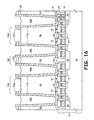
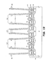
- FIGS. 8-16 and 18-20 are cross sections, and FIG. 17 is a plan view, depicting embodiments of the inventive method for forming a double-sided container capacitor structure;
- FIGS. 21 and 22 are cross sections depicting an embodiment of the invention to form a pedestal capacitor
- FIG. 23 is a block diagram of an exemplary use of the invention as a memory array in a dynamic random access memory.
- FIG. 24 is an isometric depiction of a use of the invention in an electronic device.
- wafer is to be understood as a semiconductor-based material including silicon, silicon-on-insulator (SOI) or silicon-on-sapphire (SOS) technology, doped and undoped semiconductors, epitaxial layers of, silicon supported by a base semiconductor foundation, and other semiconductor structures.
- SOI silicon-on-insulator
- SOS silicon-on-sapphire
- doped and undoped semiconductors epitaxial layers of, silicon supported by a base semiconductor foundation, and other semiconductor structures.
- previous process steps may have been utilized to form regions or junctions in or over the base semiconductor structure or foundation.
- substrate assembly may include a wafer with layers including dielectrics and conductors, and features such as transistors, formed thereover, depending on the particular stage of processing.
- the semiconductor need not be silicon-based, but could be based on silicon-germanium, silicon-on-insulator, silicon-on-sapphire, germanium, or gallium arsenide, among others.
- the term "on” used with respect to two layers, one "on” the other, means at least some contact between the layers, while “over” means the layers are in close proximity, but possibly with one or more additional intervening layers such that contact is possible but not required. Neither "on” nor “over” implies any directionality as used herein.
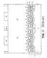
- FIG. 8 depicts a structure comprising a semiconductor wafer substrate assembly 10 comprising a semiconductor wafer 12, conductively-doped regions 14 within the wafer, transistors comprising gate oxide 18, a word line 20, silicide 22 which enhances conductivity of the word line, a dielectric transistor capping layer 24, dielectric spacers 26, and conductive contact pads 28.
- the contact pads 28 reduce the amount of dielectric which must be removed during an etch of an overlying dielectric layer.
- etch stop layer 31 is formed.
- the etch stop layer 31 may comprise a layer of silicon nitride, silicon carbon (Si•C), aluminum oxide (Al 2 O 3 ), or another material between about 50 angstroms ( ⁇ ) and about 1,000 ⁇ thick.
- a base dielectric layer 84 for example borophosphosilicate glass (BPSG), phosphosilicate glass (PSG), spun-on dielectric (SOD), or undoped silicate glass (USG), is formed over etch stop layer 31.
- a blanket support layer 86 and a blanket sacrificial layer 88 are formed over the base dielectric layer 84.
- Support layer 86 and sacrificial layer 88 include etchability of layers 88 and 84 selective to layer 86 (i.e. layers 88 and 84 can be etched while removing none or very little of layer 86).
- Layer 86 may comprise a second silicon nitride layer between about 200 ⁇ and about 1,200 ⁇ thick
- layer 88 can comprise a silicon dioxide layer, for example using a BPSG or tetraethyl orthosilicate (TEOS) process, between about 300 ⁇ and about 600 ⁇ thick, preferably about 400 ⁇ .
- a patterned etch mask 90 is formed having openings therein which allow an etch to expose contact pads 28.
- the structure of FIG. 8 is etched to remove the exposed portions of sacrificial layer 88, support layer 86, base dielectric layer 84, and etch stop layer 31, and to expose contact pads 28 and possibly a portion of capping layer 24 to result in a structure similar to FIG. 9 .
- a single etch can initially be used to remove exposed portions of sacrificial silicon dioxide layer 88, silicon nitride support layer 86, and timed to stop within base dielectric layer 84 prior to exposing etch stop 31. The chemistry can then be changed so that any remaining base dielectric layer 84 is removed while stopping on etch stop 31.
- the etch can be changed and performed for a time to sufficiently remove exposed portions of etch stop 31 which exposes contact pad 28, while not excessively etching capping layer 24 or spacers 26.
- the etch stop layer 31 may also be left in place.
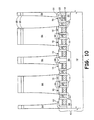
- photoresist layer 90 is removed, along with any polymer (not depicted) or other contaminants which form during the etch, to result in the structure of FIG. 10 .
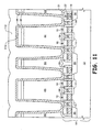
- a blanket conformal capacitor bottom plate layer 110 such as titanium nitride is formed as depicted in FIG. 11 .
- a protective layer 112 such as photoresist, is formed within the container to prevent contaminants from being deposited into the interior of the container formed by the bottom plate during subsequent processing.
- the structure is planarized, for example using chemical mechanical planarization (CMP) to result in the FIG. 12 structure.
- CMP chemical mechanical planarization
- sacrificial layer 88 is selectively etched to expose the underlying support layer 86, then protective layer 112 is removed.
- a sacrificial layer 88 of silicon dioxide can be etched selective to a silicon nitride support layer 86 and a titanium nitride bottom plate layer 110 using a wet etch comprising hydrofluoric acid (HF).
- a protective layer 112 of photoresist can be removed by ashing the material at a temperature of between about 150°C and about 300°C, and then subjecting the ash to a wet etch, for example using hydrofluoric acid (HF) to remove the photoresist ash.
- HF hydrofluoric acid
- the etch of the sacrificial layer 88 can be performed either before or after removal of protective layer 112, if the etch is selective to the material of bottom plate 110. If the etch of layer 88 is performed after removal of layer 112, the etchant may traverse any pinholes or other voids within bottom plate layer 110 and begin to etch oxide layer 84. This is not detrimental, however, as layer 84 will be removed during subsequent processing and provides no further critical function. The removal of protective layer 112 and sacrificial layer 88 results in the FIG. 13 structure.
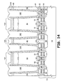
- a masking spacer layer 140 is formed over the surface of the FIG. 13 structure to result in the structure of FIG. 14 .
- the material selected for this layer must be able to withstand an etch of support layer 86, and must also be etchable selective to the material of support layer 86 and bottom plates 110. With a nitride support layer and titanium nitride bottom plates, polysilicon would function sufficiently.
- the masking spacer layer is formed to a thickness sufficient to fill in and impinge on itself in narrow regions 142, and form conformally in the wider regions 144. With current technology, the narrow regions 142 may have a width of between about 200 ⁇ and about 600 ⁇ , the wider regions 144 may have a width of between about 600 ⁇ and about 1,200 ⁇ .
- the height of the exposed portions 146 of capacitor bottom plates 110 is between about 300 ⁇ and about 600 ⁇ .
- a conformal polysilicon layer 140 is formed to have a target thickness of between about 200 ⁇ and about 500 ⁇ when measured over wide, flat surfaces.
- FIG. 14 depicts layer 140 completely filling the recess in the bottom plates, but this may not occur, depending on the size of the opening within the bottom plate. However, enough material will likely form to prevent any damage to the bottom of plates 110 during a subsequent spacer etch of layer 140 described below.
- an anisotropic spacer etch is performed on the masking spacer layer 140 to result in the FIG. 15 structure. This etch removes the material of the masking spacer layer 140 selective to the material of support layer 86 and bottom plates 110. After etching layer 140, spacers 150 remain in the wider regions 144, while layer 152 remains to bridge the narrow regions 142 formed by adjacent bottom plates 110.
- FIG. 16 is depicted in plan view along 1-1 of FIG. 17 , which depicts part of an array of container capacitor bottom plates 110 and the remaining portions 150, 152 of the masking spacer layer 140.
- FIG. 17 is depicted in plan view along 1-1 of FIG. 17 , which depicts part of an array of container capacitor bottom plates 110 and the remaining portions 150, 152 of the masking spacer layer 140.
- Various capacitor layouts other than the one depicted in FIG. 17 can be used with the present invention.
- this pattern of the masking layer defines the support layer 86
- the configuration of the support layer 86 is analogous to that of the masking spacer layer of FIG. 17 .
- the etch of the support layer 86 with this mask removes the material of support layer 86 selective to the material of bottom plates 110.
- the spacers 150 and support layer 86 can also be etched during the same operation, but it is more likely that the spacers 150 will be etched during one process and the support layer 86 will be etched during another separate etch. During the etch of support layer 86 a portion of polysilicon layer 140 and spacers 150 may also be removed, as long as enough of these two features remain to allow exposure of BPSG 84 in the wide regions 144 and protection of support layer 86 in the narrow regions 142.
- the remaining portions 140, 150, and 152 of the masking spacer layer can be removed at this point to result in the structure of FIG. 18 , or they may remain in place. If polysilicon spacers are removed, they can be etched selective to silicon nitride support layer 86 and titanium nitride bottom plates 110 using a wet etch comprising tetramethyl ammonium hydroxide (TMAH).
- TMAH tetramethyl ammonium hydroxide
- FIG. 19 depicts the structure resulting from the removal of polysilicon features 140, 150, and 152, and after etching of base dielectric layer 84.
- the base dielectric layer is removed selective to support layer 86, bottom plates 110, and etch stop 31.
- An etch which removes silicon dioxide selective to silicon nitride and titanium nitride includes a wet etch of hydrofluoric acid (HF) to result in the structure of FIG. 19 .
- HF hydrofluoric acid
- the etchant completely removes the exposed base dielectric layer 84 depicted in FIG. 17 , and removes all of dielectric 84 around each capacitor bottom plate 110.
- support structures 86 support the capacitors after removal of the base dielectric layer 84. Removal of the base dielectric layer is necessary to allow the formation of a double-sided capacitor.
- These support structures provide a dielectric collar for each bottom plate, with each collar being continuous with adjacent collars such that the support layer forms a matrix which braces all capacitor bottom plates.
- the arrangement of the support layer can be determined from FIG. 17 , which depicts the pattern of masking spacer layer 150, 152, and also of the etched support layer 86. As depicted in FIG. 19 , the top and bottom surfaces of support layer 86 are free from contact with any other layer.
- dielectric 84 may remain, especially at the point of contact between the support layer 86 and the bottom plate 110, which may be more difficult to clear completely. In any case, even if some of this dielectric 84 remains to contact the bottom side of layer 86, the top and bottom surface of support layer 86 will remain generally free from contact with any other layer. It is conceivable that for some capacitor arrangements and processes the collar may not surround the capacitor bottom plate through 360° as depicted in FIG. 17 . Further, the bottom plates or other feature being supported by the collar may not be circular as depicted in FIG. 17 , but may be oval, ovoid, square, rectangular, etc. in shape.
- a capacitor cell dielectric 200, a capacitor top plate 202, and a dielectric layer 204 are formed according to means known in the art to form the structure of FIG. 20 . Wafer processing continues according to means known in the art.
- the completed structure may have improved capacitance over conventional structures, because all of the base dielectric layer can be removed which allows the top plate to be formed along more of the bottom plate than conventional structures.
- a portion of base dielectric layer 32 must remain in place to support the capacitors during formation of the cell dielectric and top plate.
- all of the base dielectric layer can be removed as depicted in FIG. 19 , because support layer 86 remains to brace the bottom plates.
- a mask layer may be formed prior to the etch of the sacrificial dielectric layer, prior to the etch of the masking spacer layer, or prior to the etch of the support layer. This will prevent etching of BPSG over the device periphery, which would form a step in the oxide between the periphery, where there are no storage cell capacitors, and the array, where the tops of the storage cell capacitors are at the original level of the top of layer 88. If the periphery is not protected, the periphery must be backfilled with oxide which is then planarized, after forming the cell dielectric 200 and top plate 202.
- a selective etch may be performed on support layer 86 after forming spacers 152 of FIG. 16 to increase the width of the opening at 144. This larger opening may allow the base dielectric layer to be more easily removed, and may provide improved conditions for forming the cell dielectric layer 200 and capacitor top plate 202.
- a pedestal capacitor can be formed in a manner similar to the container capacitor as depicted by FIGS. 21 and 22 .
- the bottom plate layer 110 is formed to completely fill the recessed defined by the sacrificial layer 88, the support layer 86, and the base dielectric layer 84.
- the bottom plate layer 110 will be much thicker than that depicted in the FIG. 11 structure.
- protective layer 112 is not necessary, as bottom plate layer 110 completely fills the recess.
- the bottom plate layer 110 and possibly a portion of the sacrificial layer 88 is planarized to remove layer 110 from the horizontal surface of sacrificial layer 88 to leave the pedestal capacitor bottom plate 110 as depicted in FIG. 22 .
- a single layer of material may be formed instead of forming both the sacrificial layer 88 and the support layer 86 of FIG. 12 .
- This single layer would be a thicker layer of the material of the support layer, such as silicon nitride, and would be as thick as layers 86 and 88 combined.
- a timed etch would be performed on this layer to result in the structure of FIG. 13 .
- This process is not as controllable as using two separate layers and is therefore not as preferable for most process flows, but may have advantages for some processes. Processing then continues according to the other embodiments, for example to form the masking spacer layer 140 and other subsequent steps.
- FIG. 23 is a plan view depicting four arrays 230 and a periphery 232 of a semiconductor die 234 prior to forming the patterned resist layer 90 of FIG. 8 .
- a typical memory die will likely comprise a larger number of arrays.
- FIG. 24 depicts the FIG. 23 structure after forming patterned photoresist layer 90.
- Resist layer 90 has openings therein 240 which will allow the etch of the sacrificial layer 88, the support layer 86, and the base dielectric layer 84 of the FIG. 8 structure to form the FIG. 9 structure.
- FIG. 24 is not to scale, and many more openings 240 for capacitors will be formed than are depicted.
- Resist layer 90 also has openings therein 242 which form a "moat" around the array which will protect the periphery 232 during the removal of base dielectric layer 84 to form the FIG. 19 structure. This moat will be filled with material during the formation of the capacitor bottom plate 110, and thus no additional processing is required to form and fill the moat.
- the moat may be between about 200 ⁇ and about 600 ⁇ wide.
- a photoresist layer would be formed to cover and protect the periphery but to expose the array.
- the photoresist layer and the layer within the moat thereby protects the dielectric layer such as BPSG in the periphery from being etched during the removal of the base dielectric layer which exposes the sidewalls of the capacitor bottom plates.
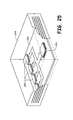
- a semiconductor device 250 formed in accordance with the invention may be attached along with other devices such as a microprocessor 252 to a printed circuit board 254, for example to a computer motherboard or as a part of a memory module used in a personal computer, a minicomputer, or a mainframe 256.
- FIG. 25 may also represent use of device 250 in other electronic devices comprising a housing 236, for example devices comprising a microprocessor 252, related to telecommunications, the automobile industry, semiconductor test and manufacturing equipment, consumer electronics, or virtually any piece of consumer or industrial electronic equipment.
- FIG. 26 is a simplified block diagram of a memory device such as a dynamic random access memory having a memory array with container capacitors which may be formed using an embodiment of the present invention.
- FIG. 26 depicts a processor 260 coupled to a memory device 262, and further depicts the following basic sections of a memory integrated circuit: control circuitry 264; row 266 and column 268 address buffers; row 270 and column 272 decoders; sense amplifiers 274; memory array 276; and data input/output 278.
Landscapes
- Engineering & Computer Science (AREA)
- Manufacturing & Machinery (AREA)
- Semiconductor Memories (AREA)
- Semiconductor Integrated Circuits (AREA)
- Chemical Vapour Deposition (AREA)
Applications Claiming Priority (2)
| Application Number | Priority Date | Filing Date | Title |
|---|---|---|---|
| US10/656,732 US7067385B2 (en) | 2003-09-04 | 2003-09-04 | Support for vertically oriented capacitors during the formation of a semiconductor device |
| EP04786595A EP1665372B1 (de) | 2003-09-04 | 2004-08-26 | Stütze für vertikal orientierte Kondensatoren während der Herstellung einer Halbleitervorrichtung |
Related Parent Applications (1)
| Application Number | Title | Priority Date | Filing Date |
|---|---|---|---|
| EP04786595.1 Division | 2004-08-26 |
Publications (2)
| Publication Number | Publication Date |
|---|---|
| EP2267768A2 true EP2267768A2 (de) | 2010-12-29 |
| EP2267768A3 EP2267768A3 (de) | 2011-03-02 |
Family
ID=34226414
Family Applications (2)
| Application Number | Title | Priority Date | Filing Date |
|---|---|---|---|
| EP10010273A Withdrawn EP2267768A3 (de) | 2003-09-04 | 2004-08-26 | Stütze für vertikal ausgerichtete Kondensatoren während der Herstellung einer Halbleitervorrichtung |
| EP04786595A Expired - Lifetime EP1665372B1 (de) | 2003-09-04 | 2004-08-26 | Stütze für vertikal orientierte Kondensatoren während der Herstellung einer Halbleitervorrichtung |
Family Applications After (1)
| Application Number | Title | Priority Date | Filing Date |
|---|---|---|---|
| EP04786595A Expired - Lifetime EP1665372B1 (de) | 2003-09-04 | 2004-08-26 | Stütze für vertikal orientierte Kondensatoren während der Herstellung einer Halbleitervorrichtung |
Country Status (8)
| Country | Link |
|---|---|
| US (3) | US7067385B2 (de) |
| EP (2) | EP2267768A3 (de) |
| JP (1) | JP4512880B2 (de) |
| KR (1) | KR20060064662A (de) |
| CN (1) | CN100587941C (de) |
| AT (1) | ATE510301T1 (de) |
| TW (1) | TWI239633B (de) |
| WO (1) | WO2005024936A2 (de) |
Families Citing this family (139)
| Publication number | Priority date | Publication date | Assignee | Title |
|---|---|---|---|---|
| US7442629B2 (en) | 2004-09-24 | 2008-10-28 | President & Fellows Of Harvard College | Femtosecond laser-induced formation of submicrometer spikes on a semiconductor substrate |
| US7057256B2 (en) | 2001-05-25 | 2006-06-06 | President & Fellows Of Harvard College | Silicon-based visible and near-infrared optoelectric devices |
| KR100506944B1 (ko) * | 2003-11-03 | 2005-08-05 | 삼성전자주식회사 | 지지층 패턴들을 채택하는 복수개의 커패시터들 및 그제조방법 |
| US7067385B2 (en) * | 2003-09-04 | 2006-06-27 | Micron Technology, Inc. | Support for vertically oriented capacitors during the formation of a semiconductor device |
| US7125781B2 (en) | 2003-09-04 | 2006-10-24 | Micron Technology, Inc. | Methods of forming capacitor devices |
| KR100546395B1 (ko) * | 2003-11-17 | 2006-01-26 | 삼성전자주식회사 | 반도체소자의 커패시터 및 그 제조방법 |
| KR100553835B1 (ko) * | 2004-01-26 | 2006-02-24 | 삼성전자주식회사 | 캐패시터 및 그 제조 방법 |
| KR100568733B1 (ko) * | 2004-02-10 | 2006-04-07 | 삼성전자주식회사 | 개선된 구조적 안정성을 갖는 캐패시터와 그 제조 방법 및이를 포함하는 반도체 장치와 그 제조 방법 |
| WO2005083790A1 (ja) * | 2004-02-27 | 2005-09-09 | Texas Instruments Japan Limited | 固体撮像装置、ラインセンサ、光センサおよび固体撮像装置の動作方法 |
| KR100545866B1 (ko) * | 2004-04-27 | 2006-01-24 | 삼성전자주식회사 | 커패시터 및 그 제조 방법 |
| US20070037349A1 (en) * | 2004-04-30 | 2007-02-15 | Martin Gutsche | Method of forming electrodes |
| KR100533959B1 (ko) * | 2004-06-30 | 2005-12-06 | 삼성전자주식회사 | 반도체 장치 제조 방법 |
| US7387939B2 (en) | 2004-07-19 | 2008-06-17 | Micron Technology, Inc. | Methods of forming semiconductor structures and capacitor devices |
| US7439152B2 (en) * | 2004-08-27 | 2008-10-21 | Micron Technology, Inc. | Methods of forming a plurality of capacitors |
| US7202127B2 (en) | 2004-08-27 | 2007-04-10 | Micron Technology, Inc. | Methods of forming a plurality of capacitors |
| US20060046055A1 (en) * | 2004-08-30 | 2006-03-02 | Nan Ya Plastics Corporation | Superfine fiber containing grey dope dyed component and the fabric made of the same |
| US7547945B2 (en) | 2004-09-01 | 2009-06-16 | Micron Technology, Inc. | Transistor devices, transistor structures and semiconductor constructions |
| KR100655751B1 (ko) * | 2004-10-01 | 2006-12-11 | 삼성전자주식회사 | 반도체 장치의 제조 방법 |
| US7320911B2 (en) | 2004-12-06 | 2008-01-22 | Micron Technology, Inc. | Methods of forming pluralities of capacitors |
| KR100752642B1 (ko) * | 2005-02-02 | 2007-08-29 | 삼성전자주식회사 | 반도체소자의 커패시터 제조방법 |
| US7557015B2 (en) | 2005-03-18 | 2009-07-07 | Micron Technology, Inc. | Methods of forming pluralities of capacitors |
| US7517753B2 (en) * | 2005-05-18 | 2009-04-14 | Micron Technology, Inc. | Methods of forming pluralities of capacitors |
| US7544563B2 (en) * | 2005-05-18 | 2009-06-09 | Micron Technology, Inc. | Methods of forming a plurality of capacitors |
| US7459362B2 (en) * | 2005-06-27 | 2008-12-02 | Micron Technology, Inc. | Methods of forming DRAM arrays |
| US7282401B2 (en) | 2005-07-08 | 2007-10-16 | Micron Technology, Inc. | Method and apparatus for a self-aligned recessed access device (RAD) transistor gate |
| US7199005B2 (en) * | 2005-08-02 | 2007-04-03 | Micron Technology, Inc. | Methods of forming pluralities of capacitors |
| US7867851B2 (en) | 2005-08-30 | 2011-01-11 | Micron Technology, Inc. | Methods of forming field effect transistors on substrates |
| US7226845B2 (en) | 2005-08-30 | 2007-06-05 | Micron Technology, Inc. | Semiconductor constructions, and methods of forming capacitor devices |
| DE102005042524A1 (de) | 2005-09-07 | 2007-03-08 | Infineon Technologies Ag | Verfahren zur Herstellung von Stapelkondensatoren für dynamische Speicherzellen |
| CN100464422C (zh) * | 2006-01-18 | 2009-02-25 | 财团法人工业技术研究院 | 空心柱型电容器及其制造方法 |
| US7700441B2 (en) | 2006-02-02 | 2010-04-20 | Micron Technology, Inc. | Methods of forming field effect transistors, methods of forming field effect transistor gates, methods of forming integrated circuitry comprising a transistor gate array and circuitry peripheral to the gate array, and methods of forming integrated circuitry comprising a transistor gate array including first gates and second grounded isolation gates |
| US20070207622A1 (en) * | 2006-02-23 | 2007-09-06 | Micron Technology, Inc. | Highly selective doped oxide etchant |
| US7557013B2 (en) * | 2006-04-10 | 2009-07-07 | Micron Technology, Inc. | Methods of forming a plurality of capacitors |
| JP4205734B2 (ja) * | 2006-05-25 | 2009-01-07 | エルピーダメモリ株式会社 | 半導体装置の製造方法 |
| US8852851B2 (en) | 2006-07-10 | 2014-10-07 | Micron Technology, Inc. | Pitch reduction technology using alternating spacer depositions during the formation of a semiconductor device and systems including same |
| US7602001B2 (en) * | 2006-07-17 | 2009-10-13 | Micron Technology, Inc. | Capacitorless one transistor DRAM cell, integrated circuitry comprising an array of capacitorless one transistor DRAM cells, and method of forming lines of capacitorless one transistor DRAM cells |
| US7666797B2 (en) | 2006-08-17 | 2010-02-23 | Micron Technology, Inc. | Methods for forming semiconductor constructions, and methods for selectively etching silicon nitride relative to conductive material |
| US7772632B2 (en) | 2006-08-21 | 2010-08-10 | Micron Technology, Inc. | Memory arrays and methods of fabricating memory arrays |
| US7589995B2 (en) | 2006-09-07 | 2009-09-15 | Micron Technology, Inc. | One-transistor memory cell with bias gate |
| US7902081B2 (en) * | 2006-10-11 | 2011-03-08 | Micron Technology, Inc. | Methods of etching polysilicon and methods of forming pluralities of capacitors |
| US7727837B2 (en) * | 2007-01-31 | 2010-06-01 | Qimonda Ag | Method of producing an integrated circuit having a capacitor with a supporting layer |
| KR100891647B1 (ko) * | 2007-02-01 | 2009-04-02 | 삼성전자주식회사 | 반도체 장치 및 그 형성 방법 |
| US7785962B2 (en) | 2007-02-26 | 2010-08-31 | Micron Technology, Inc. | Methods of forming a plurality of capacitors |
| KR100855835B1 (ko) * | 2007-03-15 | 2008-09-01 | 주식회사 하이닉스반도체 | 반도체 소자 및 그 제조 방법 |
| KR100924207B1 (ko) * | 2007-04-20 | 2009-10-29 | 주식회사 하이닉스반도체 | 반도체 소자의 제조 방법 |
| JP2008283026A (ja) * | 2007-05-11 | 2008-11-20 | Elpida Memory Inc | 半導体装置の製造方法および半導体装置 |
| DE102007022748B4 (de) * | 2007-05-15 | 2009-03-05 | Qimonda Ag | Verfahren zur Strukturierung eines Materials und strukturiertes Material |
| US7923373B2 (en) | 2007-06-04 | 2011-04-12 | Micron Technology, Inc. | Pitch multiplication using self-assembling materials |
| KR100885922B1 (ko) * | 2007-06-13 | 2009-02-26 | 삼성전자주식회사 | 반도체 소자 및 그 반도체 소자 형성방법 |
| KR100865709B1 (ko) * | 2007-06-27 | 2008-10-29 | 주식회사 하이닉스반도체 | 원통형 전하저장전극을 구비하는 캐패시터 제조 방법 |
| US7682924B2 (en) * | 2007-08-13 | 2010-03-23 | Micron Technology, Inc. | Methods of forming a plurality of capacitors |
| DE102007054077A1 (de) | 2007-11-13 | 2009-07-23 | Qimonda Ag | Verfahren zum Herstellen einer integrierten Schaltung und Anordnung mit einem Substrat |
| KR101051159B1 (ko) * | 2007-11-21 | 2011-07-21 | 주식회사 하이닉스반도체 | 반도체 소자의 형성 방법 |
| US8388851B2 (en) | 2008-01-08 | 2013-03-05 | Micron Technology, Inc. | Capacitor forming methods |
| JP2009164535A (ja) * | 2008-01-10 | 2009-07-23 | Elpida Memory Inc | 半導体装置、及びその製造方法 |
| TW200933878A (en) * | 2008-01-21 | 2009-08-01 | Ind Tech Res Inst | Memory capacitor and manufacturing method thereof |
| US7700469B2 (en) * | 2008-02-26 | 2010-04-20 | Micron Technology, Inc. | Methods of forming semiconductor constructions |
| US8274777B2 (en) | 2008-04-08 | 2012-09-25 | Micron Technology, Inc. | High aspect ratio openings |
| TWI357132B (en) * | 2008-04-09 | 2012-01-21 | Ind Tech Res Inst | Stack capacitor structure and manufacturing method |
| US7989307B2 (en) * | 2008-05-05 | 2011-08-02 | Micron Technology, Inc. | Methods of forming isolated active areas, trenches, and conductive lines in semiconductor structures and semiconductor structures including the same |
| US10151981B2 (en) | 2008-05-22 | 2018-12-11 | Micron Technology, Inc. | Methods of forming structures supported by semiconductor substrates |
| US7759193B2 (en) | 2008-07-09 | 2010-07-20 | Micron Technology, Inc. | Methods of forming a plurality of capacitors |
| KR101022670B1 (ko) * | 2008-07-18 | 2011-03-22 | 주식회사 하이닉스반도체 | 다층의 필라형 전하저장전극을 구비한 반도체장치 및 그제조 방법 |
| KR100985409B1 (ko) * | 2008-08-29 | 2010-10-06 | 주식회사 하이닉스반도체 | 반도체 장치의 캐패시터 제조 방법 |
| US20100090347A1 (en) * | 2008-10-09 | 2010-04-15 | Saylor Stephen D | Apparatus and method for contact formation in semiconductor devices |
| US7892937B2 (en) | 2008-10-16 | 2011-02-22 | Micron Technology, Inc. | Methods of forming capacitors |
| TWI375241B (en) * | 2008-10-29 | 2012-10-21 | Nanya Technology Corp | Storage node of stack capacitor and fabrication method thereof |
| US8796155B2 (en) | 2008-12-04 | 2014-08-05 | Micron Technology, Inc. | Methods of fabricating substrates |
| US8273634B2 (en) | 2008-12-04 | 2012-09-25 | Micron Technology, Inc. | Methods of fabricating substrates |
| US8247302B2 (en) * | 2008-12-04 | 2012-08-21 | Micron Technology, Inc. | Methods of fabricating substrates |
| US7951668B2 (en) * | 2009-01-14 | 2011-05-31 | Powerchip Semiconductor Corp. | Process for fabricating crown capacitors of dram and capacitor structure |
| KR101563490B1 (ko) * | 2009-03-17 | 2015-10-28 | 삼성전자주식회사 | 반도체 소자 및 그 제조 방법 |
| US8268543B2 (en) * | 2009-03-23 | 2012-09-18 | Micron Technology, Inc. | Methods of forming patterns on substrates |
| JP2010251406A (ja) * | 2009-04-13 | 2010-11-04 | Elpida Memory Inc | 半導体装置およびその製造方法 |
| US9330934B2 (en) | 2009-05-18 | 2016-05-03 | Micron Technology, Inc. | Methods of forming patterns on substrates |
| KR101179265B1 (ko) * | 2009-09-14 | 2012-09-03 | 에스케이하이닉스 주식회사 | 반도체 소자의 스토리지노드 전극 형성방법 |
| US9911781B2 (en) | 2009-09-17 | 2018-03-06 | Sionyx, Llc | Photosensitive imaging devices and associated methods |
| US9673243B2 (en) | 2009-09-17 | 2017-06-06 | Sionyx, Llc | Photosensitive imaging devices and associated methods |
| KR101616045B1 (ko) * | 2009-11-19 | 2016-04-28 | 삼성전자주식회사 | 반도체 소자 제조방법 |
| US8692198B2 (en) | 2010-04-21 | 2014-04-08 | Sionyx, Inc. | Photosensitive imaging devices and associated methods |
| CN103081128B (zh) | 2010-06-18 | 2016-11-02 | 西奥尼克斯公司 | 高速光敏设备及相关方法 |
| US8404555B2 (en) | 2010-08-10 | 2013-03-26 | Nanya Technology Corporation | Fabricating method of semiconductor device |
| US8518788B2 (en) | 2010-08-11 | 2013-08-27 | Micron Technology, Inc. | Methods of forming a plurality of capacitors |
| US8455341B2 (en) | 2010-09-02 | 2013-06-04 | Micron Technology, Inc. | Methods of forming features of integrated circuitry |
| KR20120028509A (ko) * | 2010-09-15 | 2012-03-23 | 삼성전자주식회사 | 커패시터 형성 방법 및 이를 이용한 반도체 장치 제조 방법 |
| US8222103B1 (en) * | 2011-02-15 | 2012-07-17 | Globalfoundries Inc. | Semiconductor device with embedded low-K metallization |
| KR101780050B1 (ko) | 2011-02-28 | 2017-09-20 | 삼성전자주식회사 | 반도체 기억 소자 및 반도체 기억 소자의 형성 방법 |
| US8575032B2 (en) | 2011-05-05 | 2013-11-05 | Micron Technology, Inc. | Methods of forming a pattern on a substrate |
| US9496308B2 (en) | 2011-06-09 | 2016-11-15 | Sionyx, Llc | Process module for increasing the response of backside illuminated photosensitive imagers and associated methods |
| JP2014525091A (ja) | 2011-07-13 | 2014-09-25 | サイオニクス、インク. | 生体撮像装置および関連方法 |
| US8551856B2 (en) | 2011-09-22 | 2013-10-08 | Northrop Grumman Systems Corporation | Embedded capacitor and method of fabricating the same |
| US9076680B2 (en) | 2011-10-18 | 2015-07-07 | Micron Technology, Inc. | Integrated circuitry, methods of forming capacitors, and methods of forming integrated circuitry comprising an array of capacitors and circuitry peripheral to the array |
| US8921977B2 (en) * | 2011-12-21 | 2014-12-30 | Nan Ya Technology Corporation | Capacitor array and method of fabricating the same |
| US8946043B2 (en) | 2011-12-21 | 2015-02-03 | Micron Technology, Inc. | Methods of forming capacitors |
| KR101883380B1 (ko) * | 2011-12-26 | 2018-07-31 | 삼성전자주식회사 | 커패시터를 포함하는 반도체 소자 |
| WO2013099955A1 (ja) | 2011-12-27 | 2013-07-04 | 富士フイルム株式会社 | 半導体基板製品の製造方法及びこれに利用されるエッチング方法 |
| TWI473275B (zh) * | 2012-01-04 | 2015-02-11 | Inotera Memories Inc | 具有強健型環溝結構的記憶體電容之製造方法 |
| US9177794B2 (en) | 2012-01-13 | 2015-11-03 | Micron Technology, Inc. | Methods of patterning substrates |
| JP2013153074A (ja) * | 2012-01-25 | 2013-08-08 | Fujifilm Corp | キャパシタ形成方法 |
| US9064764B2 (en) | 2012-03-22 | 2015-06-23 | Sionyx, Inc. | Pixel isolation elements, devices, and associated methods |
| KR101901787B1 (ko) | 2012-03-23 | 2018-09-28 | 삼성전자주식회사 | 반도체 기억 소자 및 반도체 기억 소자의 형성 방법 |
| KR101981724B1 (ko) * | 2012-04-18 | 2019-05-23 | 삼성전자주식회사 | 반도체 장치 및 이의 제조 방법 |
| US8629048B1 (en) | 2012-07-06 | 2014-01-14 | Micron Technology, Inc. | Methods of forming a pattern on a substrate |
| US8652926B1 (en) | 2012-07-26 | 2014-02-18 | Micron Technology, Inc. | Methods of forming capacitors |
| KR101934421B1 (ko) | 2012-11-13 | 2019-01-03 | 삼성전자 주식회사 | 반도체 소자 및 이의 제조 방법 |
| WO2014127376A2 (en) | 2013-02-15 | 2014-08-21 | Sionyx, Inc. | High dynamic range cmos image sensor having anti-blooming properties and associated methods |
| US9939251B2 (en) | 2013-03-15 | 2018-04-10 | Sionyx, Llc | Three dimensional imaging utilizing stacked imager devices and associated methods |
| WO2014209421A1 (en) | 2013-06-29 | 2014-12-31 | Sionyx, Inc. | Shallow trench textured regions and associated methods |
| KR102071528B1 (ko) | 2013-08-12 | 2020-03-02 | 삼성전자주식회사 | 일체형의 지지대를 구비한 반도체 소자 |
| US9018733B1 (en) * | 2014-03-10 | 2015-04-28 | Inotera Memories, Inc. | Capacitor, storage node of the capacitor, and method of forming the same |
| US9236446B2 (en) * | 2014-03-13 | 2016-01-12 | Taiwan Semiconductor Manufacturing Co., Ltd. | Barc-assisted process for planar recessing or removing of variable-height layers |
| US9281192B2 (en) * | 2014-03-13 | 2016-03-08 | Taiwan Semiconductor Manufacturing Co., Ltd. | CMP-friendly coatings for planar recessing or removing of variable-height layers |
| US9263577B2 (en) | 2014-04-24 | 2016-02-16 | Micron Technology, Inc. | Ferroelectric field effect transistors, pluralities of ferroelectric field effect transistors arrayed in row lines and column lines, and methods of forming a plurality of ferroelectric field effect transistors |
| US20150348963A1 (en) * | 2014-05-30 | 2015-12-03 | Inotera Memories, Inc. | Cylinder-shaped storage node with single-layer supporting structure |
| US9472560B2 (en) | 2014-06-16 | 2016-10-18 | Micron Technology, Inc. | Memory cell and an array of memory cells |
| US9159829B1 (en) | 2014-10-07 | 2015-10-13 | Micron Technology, Inc. | Recessed transistors containing ferroelectric material |
| US9305929B1 (en) | 2015-02-17 | 2016-04-05 | Micron Technology, Inc. | Memory cells |
| KR102279720B1 (ko) | 2015-06-24 | 2021-07-22 | 삼성전자주식회사 | 반도체 장치 및 그 제조 방법 |
| US10134982B2 (en) | 2015-07-24 | 2018-11-20 | Micron Technology, Inc. | Array of cross point memory cells |
| US9893083B1 (en) | 2016-10-13 | 2018-02-13 | Micron Technology, Inc. | Elevationally-extending strings of memory cells individually comprising a programmable charge storage transistor and methods of processing silicon nitride-comprising materials |
| KR102800484B1 (ko) | 2016-12-19 | 2025-04-25 | 삼성전자주식회사 | 미세 패턴 형성 방법, 커패시터 및 그의 형성 방법, 반도체 소자 및 그의 제조 방법, 반도체 소자를 포함하는 전자 시스템 |
| CN108269789B (zh) * | 2016-12-30 | 2022-05-03 | 联华电子股份有限公司 | 电容器结构及其制作方法 |
| US10396145B2 (en) * | 2017-01-12 | 2019-08-27 | Micron Technology, Inc. | Memory cells comprising ferroelectric material and including current leakage paths having different total resistances |
| US10854614B2 (en) * | 2017-12-22 | 2020-12-01 | Samsung Electronics Co., Ltd. | Semiconductor device and method of manufacturing the same |
| US11289487B2 (en) | 2018-02-23 | 2022-03-29 | Micron Technology, Inc. | Doped titanium nitride materials for DRAM capacitors, and related semiconductor devices, systems, and methods |
| CN108447864B (zh) * | 2018-03-14 | 2023-09-29 | 长鑫存储技术有限公司 | 半导体存储器件结构及其制作方法 |
| CN111326655B (zh) * | 2018-12-13 | 2023-10-17 | 夏泰鑫半导体(青岛)有限公司 | 半导体装置及其制造方法 |
| US10957699B2 (en) * | 2019-04-08 | 2021-03-23 | Micron Technology, Inc. | Integrated assemblies which include two different types of silicon nitride, and methods of forming integrated assemblies |
| US11049864B2 (en) * | 2019-05-17 | 2021-06-29 | Micron Technology, Inc. | Apparatuses including capacitor structures, and related memory devices, electronic systems, and methods |
| US11170834B2 (en) | 2019-07-10 | 2021-11-09 | Micron Technology, Inc. | Memory cells and methods of forming a capacitor including current leakage paths having different total resistances |
| CN113517273B (zh) * | 2020-04-09 | 2023-09-22 | 长鑫存储技术有限公司 | 电容器阵列结构及其制备方法和半导体存储器件 |
| EP4002504A4 (de) * | 2020-05-12 | 2023-03-01 | Changxin Memory Technologies, Inc. | Verfahren zum bilden einer kondensatoröffnung und verfahren zum bilden eines speicherkondensators |
| US11309314B2 (en) * | 2020-07-22 | 2022-04-19 | Micron Technology, Inc. | Array of capacitors and method used in forming an array of capacitors |
| CN114068415A (zh) * | 2020-07-31 | 2022-02-18 | 中国科学院微电子研究所 | 制造dram电容器的方法 |
| CN114447221A (zh) * | 2020-11-05 | 2022-05-06 | 中国科学院微电子研究所 | 电容器的制备方法 |
| CN114824080A (zh) * | 2021-01-27 | 2022-07-29 | 中国科学院微电子研究所 | 柱状电容结构、半导体器件及其制备方法 |
| CN115568209B (zh) | 2021-07-02 | 2025-11-14 | 长鑫存储技术有限公司 | 一种半导体结构及其制作方法 |
| CN116033748B (zh) * | 2023-03-24 | 2023-09-15 | 长鑫存储技术有限公司 | 半导体结构及其制备方法 |
| CN119486111A (zh) * | 2023-08-09 | 2025-02-18 | 长江存储科技有限责任公司 | 半导体结构及其制造方法、半导体器件、存储系统 |
Citations (1)
| Publication number | Priority date | Publication date | Assignee | Title |
|---|---|---|---|---|
| US20030085420A1 (en) * | 2001-11-06 | 2003-05-08 | Kabushiki Kaisha Toshiba | Semiconductor memory and method of producing the same |
Family Cites Families (112)
| Publication number | Priority date | Publication date | Assignee | Title |
|---|---|---|---|---|
| US4517729A (en) | 1981-07-27 | 1985-05-21 | American Microsystems, Incorporated | Method for fabricating MOS device with self-aligned contacts |
| US5236860A (en) * | 1991-01-04 | 1993-08-17 | Micron Technology, Inc. | Lateral extension stacked capacitor |
| US5289030A (en) | 1991-03-06 | 1994-02-22 | Semiconductor Energy Laboratory Co., Ltd. | Semiconductor device with oxide layer |
| US5467305A (en) | 1992-03-12 | 1995-11-14 | International Business Machines Corporation | Three-dimensional direct-write EEPROM arrays and fabrication methods |
| US5563089A (en) * | 1994-07-20 | 1996-10-08 | Micron Technology, Inc. | Method of forming a bit line over capacitor array of memory cells and an array of bit line over capacitor array of memory cells |
| US5340763A (en) * | 1993-02-12 | 1994-08-23 | Micron Semiconductor, Inc. | Multi-pin stacked capacitor utilizing micro villus patterning in a container cell and method to fabricate same |
| US5605857A (en) * | 1993-02-12 | 1997-02-25 | Micron Technology, Inc. | Method of forming a bit line over capacitor array of memory cells and an array of bit line over capacitor array of memory cells |
| US5401681A (en) * | 1993-02-12 | 1995-03-28 | Micron Technology, Inc. | Method of forming a bit line over capacitor array of memory cells |
| DE4447804C2 (de) | 1993-02-12 | 2002-01-24 | Micron Technology Inc | Verfahren zum Herstellen einer leitfähigen Mehrfachbehälter-Struktur auf der bestehenden Topographie eines Ausgangssubstrats |
| US5498562A (en) * | 1993-04-07 | 1996-03-12 | Micron Technology, Inc. | Semiconductor processing methods of forming stacked capacitors |
| US5784112A (en) * | 1993-07-02 | 1998-07-21 | Canon Kabushiki Kaisha | Encoding apparatus |
| US5532089A (en) | 1993-12-23 | 1996-07-02 | International Business Machines Corporation | Simplified fabrication methods for rim phase-shift masks |
| US6133620A (en) | 1995-05-26 | 2000-10-17 | Semiconductor Energy Laboratory Co., Ltd. | Semiconductor device and process for fabricating the same |
| JP2956482B2 (ja) * | 1994-07-29 | 1999-10-04 | 日本電気株式会社 | 半導体記憶装置及びその製造方法 |
| US6744091B1 (en) * | 1995-01-31 | 2004-06-01 | Fujitsu Limited | Semiconductor storage device with self-aligned opening and method for fabricating the same |
| US5654222A (en) * | 1995-05-17 | 1997-08-05 | Micron Technology, Inc. | Method for forming a capacitor with electrically interconnected construction |
| US5981992A (en) * | 1995-06-07 | 1999-11-09 | International Business Machines Corporation | Mechanical supports for very thin stacked capacitor plates |
| JPH0982918A (ja) | 1995-09-19 | 1997-03-28 | Toshiba Corp | 半導体記憶装置およびその製造方法 |
| US5990021A (en) * | 1997-12-19 | 1999-11-23 | Micron Technology, Inc. | Integrated circuit having self-aligned CVD-tungsten/titanium contact plugs strapped with metal interconnect and method of manufacture |
| US6090700A (en) | 1996-03-15 | 2000-07-18 | Vanguard International Semiconductor Corporation | Metallization method for forming interconnects in an integrated circuit |
| BR9709333A (pt) | 1996-05-21 | 1999-08-10 | Siemens Aktienesellschaft | Condensador de camadas múltiplas com alta capacidade específica e processo e produção para o mesmo |
| JPH1022476A (ja) | 1996-07-02 | 1998-01-23 | Sony Corp | 容量素子 |
| TW308727B (en) | 1996-08-16 | 1997-06-21 | United Microelectronics Corp | Semiconductor memory device with capacitor (4) |
| US5998256A (en) | 1996-11-01 | 1999-12-07 | Micron Technology, Inc. | Semiconductor processing methods of forming devices on a substrate, forming device arrays on a substrate, forming conductive lines on a substrate, and forming capacitor arrays on a substrate, and integrated circuitry |
| JP4056588B2 (ja) * | 1996-11-06 | 2008-03-05 | 富士通株式会社 | 半導体装置及びその製造方法 |
| KR19980064176A (ko) | 1996-12-17 | 1998-10-07 | 윌리엄비.켐플러 | 집적 회로 유전체 |
| US5767561A (en) | 1997-05-09 | 1998-06-16 | Lucent Technologies Inc. | Integrated circuit device with isolated circuit elements |
| US6432472B1 (en) | 1997-08-15 | 2002-08-13 | Energenius, Inc. | Method of making semiconductor supercapacitor system and articles produced therefrom |
| US6198168B1 (en) | 1998-01-20 | 2001-03-06 | Micron Technologies, Inc. | Integrated circuits using high aspect ratio vias through a semiconductor wafer and method for forming same |
| US6025225A (en) | 1998-01-22 | 2000-02-15 | Micron Technology, Inc. | Circuits with a trench capacitor having micro-roughened semiconductor surfaces and methods for forming the same |
| US5981350A (en) | 1998-05-29 | 1999-11-09 | Micron Technology, Inc. | Method for forming high capacitance memory cells |
| US5895250A (en) * | 1998-06-11 | 1999-04-20 | Vanguard International Semiconductor Corporation | Method of forming semicrown-shaped stacked capacitors for dynamic random access memory |
| US6767789B1 (en) | 1998-06-26 | 2004-07-27 | International Business Machines Corporation | Method for interconnection between transfer devices and storage capacitors in memory cells and device formed thereby |
| US6458925B1 (en) | 1998-08-03 | 2002-10-01 | University Of Maryland, Baltimore | Peptide antagonists of zonulin and methods for use of the same |
| JP4322330B2 (ja) | 1998-09-04 | 2009-08-26 | エルピーダメモリ株式会社 | 半導体集積回路装置の製造方法 |
| JP4180716B2 (ja) | 1998-12-28 | 2008-11-12 | 富士通株式会社 | 半導体装置の製造方法 |
| US6204178B1 (en) * | 1998-12-29 | 2001-03-20 | Micron Technology, Inc. | Nucleation and deposition of PT films using ultraviolet irradiation |
| US6383861B1 (en) * | 1999-02-18 | 2002-05-07 | Micron Technology, Inc. | Method of fabricating a dual gate dielectric |
| US6303956B1 (en) * | 1999-02-26 | 2001-10-16 | Micron Technology, Inc. | Conductive container structures having a dielectric cap |
| US6204143B1 (en) * | 1999-04-15 | 2001-03-20 | Micron Technology Inc. | Method of forming high aspect ratio structures for semiconductor devices |
| US6451864B1 (en) | 1999-08-17 | 2002-09-17 | Battelle Memorial Institute | Catalyst structure and method of Fischer-Tropsch synthesis |
| US6667502B1 (en) * | 1999-08-31 | 2003-12-23 | Micron Technology, Inc. | Structurally-stabilized capacitors and method of making of same |
| US6395600B1 (en) * | 1999-09-02 | 2002-05-28 | Micron Technology, Inc. | Method of forming a contact structure and a container capacitor structure |
| US6403442B1 (en) | 1999-09-02 | 2002-06-11 | Micron Technology, Inc. | Methods of forming capacitors and resultant capacitor structures |
| US6303518B1 (en) | 1999-09-30 | 2001-10-16 | Novellus Systems, Inc. | Methods to improve chemical vapor deposited fluorosilicate glass (FSG) film adhesion to metal barrier or etch stop/diffusion barrier layers |
| TW432546B (en) | 1999-11-25 | 2001-05-01 | Taiwan Semiconductor Mfg | Manufacturing method of copper damascene |
| KR20010061020A (ko) | 1999-12-28 | 2001-07-07 | 박종섭 | 반도체소자의 제조방법 |
| JP3595231B2 (ja) * | 1999-12-28 | 2004-12-02 | 株式会社東芝 | 半導体記憶装置及びその製造方法 |
| HRP20000328A2 (en) * | 2000-05-19 | 2002-02-28 | Pliva Farmaceutska Ind Dionik | Novel polymorph v of torasemide |
| KR100338775B1 (ko) | 2000-06-20 | 2002-05-31 | 윤종용 | Dram을 포함하는 반도체 소자의 콘택 구조체 및 그형성방법 |
| US6399490B1 (en) | 2000-06-29 | 2002-06-04 | International Business Machines Corporation | Highly conformal titanium nitride deposition process for high aspect ratio structures |
| DE10036725C2 (de) * | 2000-07-27 | 2002-11-28 | Infineon Technologies Ag | Verfahren zur Herstellung einer porösen Isolierschicht mit niedriger Dielektrizitätskonstante auf einem Halbleitersubstrat |
| DE10036724A1 (de) | 2000-07-27 | 2002-02-14 | Infineon Technologies Ag | Verfahren zur Bildung eines Grabens in einem Halbleitersubstrat |
| JP2002094027A (ja) | 2000-09-11 | 2002-03-29 | Toshiba Corp | 半導体記憶装置とその製造方法 |
| FR2816254B1 (fr) * | 2000-11-06 | 2003-02-07 | France Design | Toit escamotable pour vehicule a deux bras pivotants |
| US6621112B2 (en) | 2000-12-06 | 2003-09-16 | Infineon Technologies Ag | DRAM with vertical transistor and trench capacitor memory cells and methods of fabrication |
| KR100360414B1 (ko) | 2001-01-05 | 2002-11-13 | 삼성전자 주식회사 | 트윈 비트 결함을 방지하는 실린더형 커패시터의 하부전극형성방법 |
| KR100388682B1 (ko) | 2001-03-03 | 2003-06-25 | 삼성전자주식회사 | 반도체 메모리 장치의 스토리지 전극층 및 그 형성방법 |
| JP3671854B2 (ja) | 2001-04-05 | 2005-07-13 | 松下電器産業株式会社 | シリコン系基板の表面処理方法 |
| KR100422063B1 (ko) | 2001-05-02 | 2004-03-10 | 삼성전자주식회사 | 반도체 장치의 캐패시터 및 그 제조방법 |
| KR100431656B1 (ko) | 2001-09-11 | 2004-05-17 | 삼성전자주식회사 | 반도체 장치의 제조 방법 |
| JP3940576B2 (ja) | 2001-10-03 | 2007-07-04 | 有限会社アルテックスイマイデザイン | 書架における棚板の取付け装置 |
| EP1306894A1 (de) | 2001-10-19 | 2003-05-02 | Infineon Technologies AG | Verfahren zur Bildung einer Siliziumdioxidschicht auf einer gekrümmten Silizium-Oberfläche |
| KR100449030B1 (ko) * | 2002-01-24 | 2004-09-16 | 삼성전자주식회사 | 스택형 캐패시터 및 그의 제조방법 |
| US6656748B2 (en) | 2002-01-31 | 2003-12-02 | Texas Instruments Incorporated | FeRAM capacitor post stack etch clean/repair |
| KR100487519B1 (ko) | 2002-02-05 | 2005-05-03 | 삼성전자주식회사 | 반도체 장치의 커패시터 및 그 제조 방법 |
| KR100423900B1 (ko) | 2002-02-08 | 2004-03-22 | 삼성전자주식회사 | 반도체 장치의 커패시터 형성 방법 |
| US6617222B1 (en) * | 2002-02-27 | 2003-09-09 | Micron Technology, Inc. | Selective hemispherical silicon grain (HSG) conversion inhibitor for use during the manufacture of a semiconductor device |
| US6515325B1 (en) | 2002-03-06 | 2003-02-04 | Micron Technology, Inc. | Nanotube semiconductor devices and methods for making the same |
| JP4064695B2 (ja) | 2002-03-19 | 2008-03-19 | 富士通株式会社 | 半導体装置の製造方法 |
| KR100459707B1 (ko) | 2002-03-21 | 2004-12-04 | 삼성전자주식회사 | 실린더형 커패시터를 포함하는 반도체 소자 및 그 제조 방법 |
| KR100473113B1 (ko) | 2002-04-04 | 2005-03-08 | 삼성전자주식회사 | 반도체 장치의 커패시터 제조 방법 |
| JP4047631B2 (ja) | 2002-05-28 | 2008-02-13 | エルピーダメモリ株式会社 | 王冠構造のキャパシタを有する半導体集積回路装置およびその製造方法 |
| US6784479B2 (en) * | 2002-06-05 | 2004-08-31 | Samsung Electronics Co., Ltd. | Multi-layer integrated circuit capacitor electrodes |
| KR100475272B1 (ko) | 2002-06-29 | 2005-03-10 | 주식회사 하이닉스반도체 | 반도체소자 제조방법 |
| JP4353685B2 (ja) | 2002-09-18 | 2009-10-28 | 株式会社ルネサステクノロジ | 半導体装置 |
| US7341804B2 (en) | 2002-09-20 | 2008-03-11 | 3M Innovative Properties Company | Anode compositions having an elastomeric binder and an adhesion promoter |
| US6645869B1 (en) | 2002-09-26 | 2003-11-11 | Vanguard International Semiconductor Corporation | Etching back process to improve topographic planarization of a polysilicon layer |
| CA2504512A1 (en) | 2002-10-30 | 2004-05-13 | Yissum Research Development Company Of The Hebrew University Of Jerusalem | Molecules and methods using same for measuring non-transferrin bound iron |
| KR100481867B1 (ko) | 2002-11-11 | 2005-04-11 | 삼성전자주식회사 | 강유전체 커패시터 및 그 제조 방법 |
| DE10259331B4 (de) | 2002-12-18 | 2005-02-10 | Infineon Technologies Ag | Herstellungsverfahren für eine Photomaske für eine integrierte Schaltung und entsprechende Photomaske |
| JP4502173B2 (ja) | 2003-02-03 | 2010-07-14 | ルネサスエレクトロニクス株式会社 | 半導体装置及びその製造方法 |
| TW578328B (en) | 2003-03-28 | 2004-03-01 | Gemtek Technology Co Ltd | Dual-frequency inverted-F antenna |
| US6981992B2 (en) * | 2003-04-09 | 2006-01-03 | American Prosthetic Components, Inc. | Three prong adapter |
| US6720232B1 (en) * | 2003-04-10 | 2004-04-13 | Taiwan Semiconductor Manufacturing Company | Method of fabricating an embedded DRAM for metal-insulator-metal (MIM) capacitor structure |
| JP2005032982A (ja) * | 2003-07-14 | 2005-02-03 | Renesas Technology Corp | 半導体装置 |
| US6784069B1 (en) | 2003-08-29 | 2004-08-31 | Micron Technology, Inc. | Permeable capacitor electrode |
| US7067385B2 (en) * | 2003-09-04 | 2006-06-27 | Micron Technology, Inc. | Support for vertically oriented capacitors during the formation of a semiconductor device |
| US7125781B2 (en) | 2003-09-04 | 2006-10-24 | Micron Technology, Inc. | Methods of forming capacitor devices |
| DE10344814B3 (de) | 2003-09-26 | 2005-07-14 | Infineon Technologies Ag | Speichervorrichtung zur Speicherung elektrischer Ladung und Verfahren zu deren Herstellung |
| KR100546395B1 (ko) | 2003-11-17 | 2006-01-26 | 삼성전자주식회사 | 반도체소자의 커패시터 및 그 제조방법 |
| US7019346B2 (en) | 2003-12-23 | 2006-03-28 | Intel Corporation | Capacitor having an anodic metal oxide substrate |
| KR100568733B1 (ko) * | 2004-02-10 | 2006-04-07 | 삼성전자주식회사 | 개선된 구조적 안정성을 갖는 캐패시터와 그 제조 방법 및이를 포함하는 반도체 장치와 그 제조 방법 |
| AU2005263057B2 (en) | 2004-07-08 | 2009-07-23 | Lg Electronics Inc. | Method for allocating electronic serial number for mobile station |
| US7387939B2 (en) | 2004-07-19 | 2008-06-17 | Micron Technology, Inc. | Methods of forming semiconductor structures and capacitor devices |
| US20060024958A1 (en) | 2004-07-29 | 2006-02-02 | Abbas Ali | HSQ/SOG dry strip process |
| US7160788B2 (en) | 2004-08-23 | 2007-01-09 | Micron Technology, Inc. | Methods of forming integrated circuits |
| US7439152B2 (en) | 2004-08-27 | 2008-10-21 | Micron Technology, Inc. | Methods of forming a plurality of capacitors |
| US7202127B2 (en) | 2004-08-27 | 2007-04-10 | Micron Technology, Inc. | Methods of forming a plurality of capacitors |
| US20060046055A1 (en) * | 2004-08-30 | 2006-03-02 | Nan Ya Plastics Corporation | Superfine fiber containing grey dope dyed component and the fabric made of the same |
| US7320911B2 (en) * | 2004-12-06 | 2008-01-22 | Micron Technology, Inc. | Methods of forming pluralities of capacitors |
| US7557015B2 (en) | 2005-03-18 | 2009-07-07 | Micron Technology, Inc. | Methods of forming pluralities of capacitors |
| US7517753B2 (en) | 2005-05-18 | 2009-04-14 | Micron Technology, Inc. | Methods of forming pluralities of capacitors |
| US7544563B2 (en) | 2005-05-18 | 2009-06-09 | Micron Technology, Inc. | Methods of forming a plurality of capacitors |
| US7491650B2 (en) | 2005-07-27 | 2009-02-17 | Micron Technology, Inc. | Etch compositions and methods of processing a substrate |
| US7199005B2 (en) | 2005-08-02 | 2007-04-03 | Micron Technology, Inc. | Methods of forming pluralities of capacitors |
| US7713813B2 (en) | 2005-08-31 | 2010-05-11 | Micron Technology, Inc. | Methods of forming capacitors |
| US20070099328A1 (en) | 2005-10-31 | 2007-05-03 | Yuan-Sheng Chiang | Semiconductor device and interconnect structure and their respective fabricating methods |
| US20070207622A1 (en) * | 2006-02-23 | 2007-09-06 | Micron Technology, Inc. | Highly selective doped oxide etchant |
| US7557013B2 (en) | 2006-04-10 | 2009-07-07 | Micron Technology, Inc. | Methods of forming a plurality of capacitors |
| US7902081B2 (en) * | 2006-10-11 | 2011-03-08 | Micron Technology, Inc. | Methods of etching polysilicon and methods of forming pluralities of capacitors |
| US7682924B2 (en) * | 2007-08-13 | 2010-03-23 | Micron Technology, Inc. | Methods of forming a plurality of capacitors |
-
2003
- 2003-09-04 US US10/656,732 patent/US7067385B2/en not_active Expired - Fee Related
-
2004
- 2004-08-26 EP EP10010273A patent/EP2267768A3/de not_active Withdrawn
- 2004-08-26 AT AT04786595T patent/ATE510301T1/de not_active IP Right Cessation
- 2004-08-26 KR KR1020067004417A patent/KR20060064662A/ko not_active Ceased
- 2004-08-26 JP JP2006525367A patent/JP4512880B2/ja not_active Expired - Fee Related
- 2004-08-26 CN CN200480032909A patent/CN100587941C/zh not_active Expired - Fee Related
- 2004-08-26 EP EP04786595A patent/EP1665372B1/de not_active Expired - Lifetime
- 2004-08-26 WO PCT/US2004/027898 patent/WO2005024936A2/en not_active Ceased
- 2004-09-03 TW TW093126719A patent/TWI239633B/zh not_active IP Right Cessation
-
2005
- 2005-03-10 US US11/077,388 patent/US7655968B2/en not_active Expired - Fee Related
-
2010
- 2010-01-19 US US12/689,955 patent/US8786001B2/en not_active Expired - Fee Related
Patent Citations (1)
| Publication number | Priority date | Publication date | Assignee | Title |
|---|---|---|---|---|
| US20030085420A1 (en) * | 2001-11-06 | 2003-05-08 | Kabushiki Kaisha Toshiba | Semiconductor memory and method of producing the same |
Also Published As
| Publication number | Publication date |
|---|---|
| US20050158949A1 (en) | 2005-07-21 |
| US20050051822A1 (en) | 2005-03-10 |
| US7655968B2 (en) | 2010-02-02 |
| TW200518315A (en) | 2005-06-01 |
| CN1879211A (zh) | 2006-12-13 |
| KR20060064662A (ko) | 2006-06-13 |
| WO2005024936A3 (en) | 2005-04-21 |
| JP4512880B2 (ja) | 2010-07-28 |
| US7067385B2 (en) | 2006-06-27 |
| EP1665372B1 (de) | 2011-05-18 |
| ATE510301T1 (de) | 2011-06-15 |
| EP2267768A3 (de) | 2011-03-02 |
| CN100587941C (zh) | 2010-02-03 |
| WO2005024936B1 (en) | 2005-08-04 |
| EP1665372A2 (de) | 2006-06-07 |
| US20100117196A1 (en) | 2010-05-13 |
| WO2005024936A2 (en) | 2005-03-17 |
| TWI239633B (en) | 2005-09-11 |
| US8786001B2 (en) | 2014-07-22 |
| JP2007534145A (ja) | 2007-11-22 |
Similar Documents
| Publication | Publication Date | Title |
|---|---|---|
| EP1665372B1 (de) | Stütze für vertikal orientierte Kondensatoren während der Herstellung einer Halbleitervorrichtung | |
| US7683413B2 (en) | Double sided container capacitor for a semiconductor device | |
| US7125781B2 (en) | Methods of forming capacitor devices | |
| US8546215B2 (en) | Methods of fabricating a memory device | |
| US7547938B2 (en) | Semiconductor devices having elongated contact plugs | |
| JP2001189438A (ja) | 半導体記憶装置及びその製造方法 | |
| US5930621A (en) | Methods for forming vertical electrode structures and related structures | |
| US6642135B2 (en) | Method for forming semiconductor memory device having a fuse | |
| US6607954B2 (en) | Methods of fabricating cylinder-type capacitors for semiconductor devices using a hard mask and a mold layer | |
| US6943081B2 (en) | Method of forming storage nodes comprising a base in a contact hole and related structures | |
| US20020140018A1 (en) | Method of manufacturing semiconductor device having storage electrode of capacitor | |
| US6680502B2 (en) | Buried digit spacer separated capacitor array | |
| KR100674894B1 (ko) | 2단계 화학기계적 연마를 통한 하부전극층 분리방법 | |
| KR100609535B1 (ko) | 반도체소자의 캐패시터 형성방법 | |
| US20080050878A1 (en) | Method for preparing a memory structure | |
| KR20010021422A (ko) | 반도체메모리장치 및 그 제조방법 | |
| US20080044970A1 (en) | Memory structure and method for preparing the same | |
| KR20030004584A (ko) | 반도체 메모리 장치의 스토리지 전극 형성 방법 | |
| KR20080010125A (ko) | 반도체 소자의 커패시터 제조 방법 |
Legal Events
| Date | Code | Title | Description |
|---|---|---|---|
| PUAI | Public reference made under article 153(3) epc to a published international application that has entered the european phase |
Free format text: ORIGINAL CODE: 0009012 |
|
| AC | Divisional application: reference to earlier application |
Ref document number: 1665372 Country of ref document: EP Kind code of ref document: P |
|
| AK | Designated contracting states |
Kind code of ref document: A2 Designated state(s): AT BE BG CH CY CZ DE DK EE ES FI FR GB GR HU IE IT LI LU MC NL PL PT RO SE SI SK TR |
|
| RIN1 | Information on inventor provided before grant (corrected) |
Inventor name: MANNING, MONTOGMERY H. |
|
| RIN1 | Information on inventor provided before grant (corrected) |
Inventor name: MANNING, MONTGOMERY H. |
|
| PUAL | Search report despatched |
Free format text: ORIGINAL CODE: 0009013 |
|
| AK | Designated contracting states |
Kind code of ref document: A3 Designated state(s): AT BE BG CH CY CZ DE DK EE ES FI FR GB GR HU IE IT LI LU MC NL PL PT RO SE SI SK TR |
|
| 17P | Request for examination filed |
Effective date: 20110728 |
|
| 17Q | First examination report despatched |
Effective date: 20111123 |
|
| STAA | Information on the status of an ep patent application or granted ep patent |
Free format text: STATUS: THE APPLICATION IS DEEMED TO BE WITHDRAWN |
|
| 18D | Application deemed to be withdrawn |
Effective date: 20160229 |