EP2267841A1 - Antenne à fentes avec guide d'onde d'alimentation et procédé de fabrication d'une telle antenne - Google Patents
Antenne à fentes avec guide d'onde d'alimentation et procédé de fabrication d'une telle antenne Download PDFInfo
- Publication number
- EP2267841A1 EP2267841A1 EP10165653A EP10165653A EP2267841A1 EP 2267841 A1 EP2267841 A1 EP 2267841A1 EP 10165653 A EP10165653 A EP 10165653A EP 10165653 A EP10165653 A EP 10165653A EP 2267841 A1 EP2267841 A1 EP 2267841A1
- Authority
- EP
- European Patent Office
- Prior art keywords
- metalized layer
- radiating
- antenna
- waveguide
- layer
- Prior art date
- Legal status (The legal status is an assumption and is not a legal conclusion. Google has not performed a legal analysis and makes no representation as to the accuracy of the status listed.)
- Granted
Links
- 238000000034 method Methods 0.000 title claims description 33
- 239000000758 substrate Substances 0.000 claims abstract description 70
- 230000008878 coupling Effects 0.000 claims abstract description 39
- 238000010168 coupling process Methods 0.000 claims abstract description 39
- 238000005859 coupling reaction Methods 0.000 claims abstract description 39
- 239000003989 dielectric material Substances 0.000 claims abstract description 8
- 230000005670 electromagnetic radiation Effects 0.000 claims abstract description 6
- 239000010410 layer Substances 0.000 claims description 124
- 238000001465 metallisation Methods 0.000 claims description 30
- 239000012790 adhesive layer Substances 0.000 claims description 12
- 239000011248 coating agent Substances 0.000 claims description 8
- 238000000576 coating method Methods 0.000 claims description 8
- 239000004020 conductor Substances 0.000 claims description 8
- 230000002452 interceptive effect Effects 0.000 claims description 4
- 239000007769 metal material Substances 0.000 claims description 3
- RYGMFSIKBFXOCR-UHFFFAOYSA-N Copper Chemical compound [Cu] RYGMFSIKBFXOCR-UHFFFAOYSA-N 0.000 description 10
- 239000010949 copper Substances 0.000 description 10
- 229910052802 copper Inorganic materials 0.000 description 10
- 229920005989 resin Polymers 0.000 description 6
- 239000011347 resin Substances 0.000 description 6
- 238000003491 array Methods 0.000 description 5
- 238000004519 manufacturing process Methods 0.000 description 5
- 239000004411 aluminium Substances 0.000 description 4
- 229910052782 aluminium Inorganic materials 0.000 description 4
- XAGFODPZIPBFFR-UHFFFAOYSA-N aluminium Chemical compound [Al] XAGFODPZIPBFFR-UHFFFAOYSA-N 0.000 description 4
- 229910052751 metal Inorganic materials 0.000 description 3
- 239000002184 metal Substances 0.000 description 3
- 239000003822 epoxy resin Substances 0.000 description 2
- 238000003801 milling Methods 0.000 description 2
- 229920000647 polyepoxide Polymers 0.000 description 2
- 229920001410 Microfiber Polymers 0.000 description 1
- 239000000853 adhesive Substances 0.000 description 1
- 230000001070 adhesive effect Effects 0.000 description 1
- 230000005540 biological transmission Effects 0.000 description 1
- 230000015572 biosynthetic process Effects 0.000 description 1
- 238000005219 brazing Methods 0.000 description 1
- 238000005520 cutting process Methods 0.000 description 1
- 230000000593 degrading effect Effects 0.000 description 1
- 230000001419 dependent effect Effects 0.000 description 1
- 238000010586 diagram Methods 0.000 description 1
- 238000005553 drilling Methods 0.000 description 1
- 230000000694 effects Effects 0.000 description 1
- 239000011521 glass Substances 0.000 description 1
- 239000003292 glue Substances 0.000 description 1
- PCHJSUWPFVWCPO-UHFFFAOYSA-N gold Chemical compound [Au] PCHJSUWPFVWCPO-UHFFFAOYSA-N 0.000 description 1
- 239000010931 gold Substances 0.000 description 1
- 229910052737 gold Inorganic materials 0.000 description 1
- 230000001678 irradiating effect Effects 0.000 description 1
- 239000000463 material Substances 0.000 description 1
- 239000003658 microfiber Substances 0.000 description 1
- 238000001259 photo etching Methods 0.000 description 1
- 239000004033 plastic Substances 0.000 description 1
- 238000007747 plating Methods 0.000 description 1
- 230000001681 protective effect Effects 0.000 description 1
- 229910052709 silver Inorganic materials 0.000 description 1
- 239000004332 silver Substances 0.000 description 1
Images


Classifications
-
- H—ELECTRICITY
- H01—ELECTRIC ELEMENTS
- H01Q—ANTENNAS, i.e. RADIO AERIALS
- H01Q21/00—Antenna arrays or systems
- H01Q21/0006—Particular feeding systems
- H01Q21/0037—Particular feeding systems linear waveguide fed arrays
- H01Q21/0043—Slotted waveguides
- H01Q21/005—Slotted waveguides arrays
-
- H—ELECTRICITY
- H01—ELECTRIC ELEMENTS
- H01P—WAVEGUIDES; RESONATORS, LINES, OR OTHER DEVICES OF THE WAVEGUIDE TYPE
- H01P3/00—Waveguides; Transmission lines of the waveguide type
- H01P3/12—Hollow waveguides
- H01P3/121—Hollow waveguides integrated in a substrate
-
- H—ELECTRICITY
- H01—ELECTRIC ELEMENTS
- H01Q—ANTENNAS, i.e. RADIO AERIALS
- H01Q13/00—Waveguide horns or mouths; Slot antennas; Leaky-waveguide antennas; Equivalent structures causing radiation along the transmission path of a guided wave
- H01Q13/20—Non-resonant leaky-waveguide or transmission-line antennas; Equivalent structures causing radiation along the transmission path of a guided wave
- H01Q13/22—Longitudinal slot in boundary wall of waveguide or transmission line
Definitions
- the present invention concerns the technical field of antennas for telecommunication systems and in particular it refers to a slot array antenna with waveguide feed and to a process for making said antenna.
- the slot array antennas with waveguide feed are currently widely used in navigation systems, in radar systems and in other telecommunications applications, for example in aeronautical and missile-related applications.
- Such antennas generally comprise one or more radiating waveguides having a plurality of radiating slots, provided for irradiating electromagnetic radiation, and each having at least one coupling slot provided for operatively coupling the radiating waveguide with a feeding waveguide, so as to be able to feed the radiating waveguide, and therefore the radiating slots, with electromagnetic radiation.
- the same antenna is used both to transmit and to receive, for which reason when receiving, by exploiting the reciprocity of the antenna, the radiating slots are used to receive electromagnetic radiation reflected from a target.
- Slot array antennas with waveguide feed for aeronautical, radar and missile-related applications are generally made using radiating waveguides having a structure made from aluminium, in which the radiating slots and the coupling slots are through openings made respectively in the upper and lower walls of the guide and obtained through electro-erosion techniques or through laser or mechanical processing.
- the state of the art also includes a way of making slot array antennas with waveguide feed in accordance with which it is foreseen for the radiating slot array to be made on a sheet of copper, making through openings on such a sheet through photolithographic techniques.
- the radiating waveguides are made as blocks of copper or aluminium with an essentially U-shaped section that are fixedly connected to the sheet through relatively expensive and complicated techniques, like for example dip brazing.
- the process for manufacturing the antenna described in the aforementioned article is therefore relatively complex, because it is clearly necessary to take into account a delicate alignment and because the layer of resin must be shaped so as to follow the profile of the coupling slots (indicated in the aforementioned article as "feed slots") made on the lower face of the first substrate. Moreover, it is practically impossible to deterministically establish the shape of the layer of conductive resin after polymerisation since it is different to the initial one of the resin in plastic state. For this reason, it may be the case that the coupling slots are partially covered by such a resin, which means possible losses and mismatching.
- Patent application FR 2 778 024 describes a connection structure for dielectric waveguides. It is considered that this document is unable to give a man skilled in the art any suggestion on improving the problem of coupling present in the antenna described in the aforementioned article, also because the described connection structure would require the coupling slots to be made inclined both on the lower substrate and on the upper one and would require such substrates to be aligned very accurately before coupling them so as to match up corresponding pairs of coupling slots, which would make the manufacturing process relatively more complex. Whenever the alignment is not accurate, there will be losses similar to those of the antenna described in the aforementioned article.
- the purpose of the present invention is to provide a slot array antenna with waveguide feed that is able to be made through a process that is able to overcome the drawbacks indicated above with reference to the manufacturing techniques of the state of the art described above.
- An object of the present invention is also a process for making a slot array antenna with waveguide feed as defined in claim 8 in its general form and in the subsequent claims in particular embodiments.
- An object of the present invention is also a double-band antenna as described in claim 15.
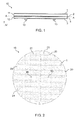
- reference numeral 10 globally indicates a slot array antenna with waveguide feed.
- the antenna 10 is for example part of a telecommunications system, like for example an automatic guidance system or a radar system comprising a transmission and/or reception system operatively connected to such an antenna, not shown in the figures.
- the antenna 10 is an antenna operating in KA band.
- the antenna 10 represented in the attached figures has a multi-layer structure and comprises:
- the antenna 10 also comprises four feeding connectors 13, for example in waveguide, only two of which can be seen in figure 1 .
- the metalized layers 1, 2 are two layers that are laminated/plated and more preferably electrodeposited on the two opposite faces of the first dielectric substrate 11.
- the metalized layers 1, 2 are made from copper and have, for example, a thickness equal to about 8-20 micron and more preferably equal to about 8 micron.
- the first dielectric substrate 11 is, for example, a commercial substrate made from reinforced glass microfibre with a relatively low dielectric constant, for example within the range 2 - 3 and more preferably equal to about 2.2.
- the first substrate 11 has a thickness equal to about 1mm.
- a substrate 11 of the aforementioned type is, for example, currently produced by TaconicTM and marketed with the name "TLY - 5A" and it is supplied by the aforementioned producer with the copper layers 1 and 2 already electrodeposited.
- the second dielectric substrate 12 is also of the type described above with reference to the first dielectric substrate 11, with the sole difference that the second dielectric substrate 12, instead of having a metallisation layer on both faces, has a free face, i.e. a face on which no metallisation is foreseen.
- the metallisation layer 3 which is for example a laminated/plated layer and more preferably a layer of electrodeposited copper of the type already described with reference to the metalized layers 1 and 2.
- the second substrate 12 is also currently produced by TaconicTM and marketed with the name "TLY - 5A" and it is supplied by the aforementioned producer with the copper layer 3 electrodeposited and with a free face, i.e. without a metallisation layer.
- the second dielectric substrate 12 with the electrodeposited copper layer 3 can be obtained from a substrate with two opposite metallisation layers (like the substrate 11) by removing one of said layers.
- first 11 and the second 12 dielectric substrate are laminated dielectric substrates with surface metallization as described above but produced and marketed by Rogers Corporation with the trade name DuroidTM 5880.
- the layer 4 is a thin adhesive layer used to keep together the two laminated dielectric substrates 11 and 12 and in particular used to glue the free face of the second substrate 12 to the free face of the metallisation layer 2.
- the adhesive layer 4 is a thin dielectric film, therefore electrically insulating, for example like the one currently marketed with the name "NeltecTM 6700".
- the dielectric properties of such an adhesive layer 4 are advantageously as similar as possible to those of the second dielectric substrate 12.
- the slot array antenna 10 comprises at least one radiating waveguide 20 comprising a plurality, or an array, of radiating slots 21.
- the slot array antenna 10 comprises, without for this reason introducing any limitation, forty radiating waveguides 20, of different lengths and having a variable number of slots based on the respective length. It should be observed that the particular example described is in the form of a planar antenna having slot array with symmetry in quadrants and more specifically a monopulse antenna.
- a slot array antenna 10 comprising a plurality of radiating waveguides 20.
- the radiating waveguides 20 are made in the first dielectric substrate 11, which therefore houses them, and the first 1 and the second 2 metalized layer represent opposite confinement walls, upper and lower respectively, of the radiating waveguides 20.
- the radiating slots 21 are openings, in the example substantially rectangular in shape, made in the first metalized layer 1, preferably through photolithographic techniques of selective removal of the metallisation layer 1 at the points in which it is wished to make the radiating slots 21.
- Photolithographic techniques are commonly used in making printed circuits and they are part of the background knowledge of a man skilled in the art, and for this reason they will not be detailed any further in the present description.
- the aforementioned selective removal of the metallization is carried out using a laser device. It should be noted that the free face of the metalized layer 1 in practice represents the radiating surface of the antenna.
- each of the radiating waveguides 20 comprises at least one coupling slot 31, provided for operatively coupling the radiating waveguide 20 with a feeding waveguide, so as to be adapted to feed the radiating waveguide 20, and therefore the radiating slots 21, with electromagnetic radiation.
- the coupling slots 31 are also openings, in the example substantially rectangular in shape, made in the second metalized layer 2, preferably through photolithographic techniques that adopt a selective removal of the metallization 2 at the points in which it is wished to make the coupling slots 31.
- the coupling slots 31 are openings that are substantially rectangular in shape, and the inclination of which varies among the different radiating waveguides 20.
- the aforementioned selective removal of the metallization is carried out using a laser device or through mechanical processing.
- each radiating guide 20 comprises side confinement walls 23, 24.
- Such side confinement walls 23, 24 are each formed by a respective array of through channels 22.
- the confinement walls 23, 24, although consisting of discreet and spaced elements 22, can be considered as approximately continuous side confinement walls.
- the through channels 22 are for example obtained by perforating, for example drilling, the first metalized layer 1, the first dielectric substrate 11 and the second metalized layer 2.
- the channels 22 thus made are then preferably plated with a copper inner surface coating.
- the diameter of the channels 22 is equal to about 0.4 mm and the processing tolerance of the perforation is advantageously equal to +/- 0.005mm. On the position of the channel holes 22, the tolerance is advantageously equal to +/- 0.03 mm. Obviously, these processing parameters can be varied based upon the working frequency for which the slot array antenna 10 is designed.
- the processing steps described above with reference to the formation of the radiating waveguides 20, of the radiating slots 21 and of the coupling slot are carried out on a first dielectric substrate 11 laminated/plated on both faces, before coupling such a first dielectric substrate 11, through an electrically insulating adhesive layer 4, with the dielectric substrate 12 laminated/plated just on one of the two faces. Thereafter, indeed, the first 11 and the second 12 dielectric substrate are coupled, through the electrically insulating adhesive layer 4, so that the non-plated face of the second dielectric substrate 12 faces the metallisation layer 2.
- the slot array antenna 10 comprises at least one feeding waveguide 40, 41, 42, 43 of the radiating guides 20 operatively coupled with them through the coupling slots 31.
- four feeding waveguides 40, 41, 42, 43 are provided each intended to independently feed a respective group of ten radiating waveguides 20.
- the feeding waveguides 40, 41, 42, 43 are oriented transversally with respect to the radiating waveguides 20. Henceforth we shall refer, without for this reason introducing any limitation, to the case in which the slot array antenna 10 comprises a plurality of feeding waveguides 40, 41, 42, 43.
- the feeding waveguides 40, 41, 42, 43 are advantageously made in the second dielectric substrate 12, which therefore houses them, preferably making blind grooves 44-48, preferably through mechanical processing and alternatively through laser processing, advantageously in parallel sets of two, in the second dielectric substrate 12, preferably going from the metallisation layer 3, entirely crossing such a layer 3, also entirely crossing the second dielectric substrate 12, the dielectric adhesive layer 4 and coming to partially cover (i.e. partially cross) also the second metalized layer 2.
- This explains why the feeding waveguides 40, 41, 42, 43 are (partially) visible in figure 3 , since the blind grooves 44-48 that partially cross the metallisation layer 2 are indeed visible.
- FIG 6 which shows a side section of the portion of the antenna 10 defined by the dashed square 35 in figure 3 (section along the axis Y-Y), in which it is in practice possible to see a cross section of the feeding waveguide 42, the blind grooves 44-48 thus obtained are surface coated, i.e. plated, with a conductive metallization 60 to form the side confinement walls of the feeding waveguides 40-43.
- the upper and lower confinement walls of the feeding waveguides 40-43 will consist of the metalized layers 2 and 3.
- the upper confinement wall of the feeding waveguides coincides with the metallisation layer 2, which represents the lower confinement wall of the radiating waveguides 20.
- Such a wall is therefore a confinement wall, or layer, shared among the radiating waveguides and the feeding waveguides.
- the lower face of such a wall represents the upper conductive confinement surface of the feeding waveguides and the upper face of such a wall represents the lower conductive confinement surface of the radiating waveguides 20.
- the slot array antenna 10 also comprises at least one input slot 49 for each feeding waveguide 40-43. It should be observed that in figure 6 the input slot 49 has been represented purely as an example, since from the joint viewing of figures 3 and 4 it can be seen how in the section along the axis Y-Y there isn't any input slot 49.
- the input slots 49 are openings, for example substantially rectangular in shape, made in the third metalized layer 3, preferably through photolithographic techniques that foresee a selective removal of the metallisation layer 3 at the points in which it is wished to make the input slots 49.
- the slot array antenna also includes a plurality of through channels 50 that extend from the free face of the metalized layer 1 to the free face of the metalized layer 3.
- Such through channels 50 are aligned in arrays of channels, arranged in sets of two, a relatively small distance apart with respect to the wavelength, and they are coated or filled with conductive material, such as copper, to separate two or more feeding waveguides 40-43 from one another.
- an array 50 of through channels divides the feeding waveguide defined by the blind plated grooves 46, 47 in two feeding waveguides 40, 41 and how, in an analogous manner, an array 50 of through channels divides the feeding waveguide defined by the blind and plated grooves 44, 45 in the two feeding waveguides 42, 43. It should be observed how in the described example, such through channels 50 are arranged, exploiting the available space, between adjacent waveguides, so as not to interfere with them, therefore avoiding influencing the propagative characteristics.
- the slot array antenna 10 also comprises a plurality of blind holes 51, to allow the same antenna to have connectors fixed to it, for example in waveguide, adapted for feeding the feeding waveguides 40-43.
- blind holes advantageously, are not plated and extend from the metallisation layer 2 to the metallisation layer 3.
- four groups are provided comprising four holes 51 each to allow each of the feeding waveguides 40-43 to be coupled with a respective connector.
- the process globally indicated with 100, comprises a first step 101 of providing the first plate-shaped dielectric substrate 11 having two opposite metalized faces, i.e. equipped with two surface metallisation layers 1, 2.
- a dielectric substrate 11 of the type indicated above has already been described with reference to figures 1-6 and therefore it will not be detailed any further.
- the first step 101 comprises an operation of providing the second plate-shaped dielectric substrate 12, as already described earlier, equipped with a free face and with an opposite metalized face, i.e. coupled with the metallisation layer 3.
- the process 100 also comprises a step 102 including an operation of making at least one radiating slot array 21 by selectively removing, preferably photolithographically, said portions of the first metalized layer 1 and an operation of making at least one coupling slot 31 by selectively removing, preferably photolithographically at least one portion of the second metalized layer 2.
- a step 102 including an operation of making at least one radiating slot array 21 by selectively removing, preferably photolithographically, said portions of the first metalized layer 1 and an operation of making at least one coupling slot 31 by selectively removing, preferably photolithographically at least one portion of the second metalized layer 2.
- the selective removal of portions of the metalized layers 1 and 2 takes place through laser techniques.
- the process 100 also comprises a step 103 comprising an operation of making a plurality of through channels 22 that extend from the first 1 to the second 2 metalized layer and an operation of surface coating inner walls of said channels 22, or of filling such through channels 22 with an electrically conductive material, so that the through channels 22 thus filled or coated define side confinement walls of at least one radiating waveguide 10, the first 1 and the second 2 metallisation layer representing two further opposite confinement walls of the aforementioned at least one radiating waveguide 20.
- the aforementioned through channels 22 are obtained by perforating the first metalized layer 1, the first dielectric substrate 11 and the second metalized layer 2, for example through a mechanical perforation device.
- the process 100 also comprises:
- an operation of selectively increasing the thickness of the second metalized layer 2 is carried out, for example galvanically, in the areas in which it has not been removed to make the coupling slots 41.
- an enlargement operation is such as to bring the metalized layer 2 from a thickness of about 8-20 micron to a thickness of about 40-70 micron.
- the step 105 of making the blind grooves 44-47 can be carried out in a simple manner, for example with a relatively small precision milling cutter, without running the risk of completely perforating the metalized layer 2.
- the process 100 also comprises a step 105 of making at least one input slot 49 by removing, preferably photolithographically, at least one portion of the third metalized layer 3 and preferably also a step of making one or more arrays of through channels 50 that pass through the entire multi-layer structure as made above and of internally metalizing said arrays of through channels 50 to divide at least one feeding waveguide (40-43) into two or more operatively separate feeding waveguides.
- the process 100 also preferably comprises a step 106 of making one or more groups of non-through holes 51 to couple one or more input connecters with the multi-layer structure as obtained above on the side of the third metallisation layer 3.
- the process 100 also preferably comprises a step 107 of selectively plating the exposed metalized parts with a layer of protective material, for example with gold.
- the antenna 10 has a compact structure in terms of vertical dimensions and is relatively light and does not have the problems of losses due to the coupling between the two substrates described with reference to the prior art.
- the radiating guides are made from a substrate of dielectric material (i.e. such guides are "loaded"), such guides can have a relatively small width (by width we mean the longer side of the section of the guide) and they make it possible to make distances of positioning of two consecutive slots inside the same guide that for the same working frequency are relatively smaller than those of the air guides of the prior art. For this reason, therefore, for the same planar dimensions of the antenna it is possible to make an antenna having a greater number of guides and/or guides with a greater number of radiating slots therefore obtaining, for the same planar dimensions, an improvement in performance in terms of directivity and gain.
- the antenna 10 as described with reference to figures 1-6 , in which the connectors 13 are not provided has a monopulse comparator 80 that is operatively connected to the input slots 49 coupled with it on the side of the metalized layer 3.
- the monopulse comparator 80 is a waveguide comparator, made on a dielectric substrate 81 analogous to the substrate 11 described above (therefore equipped with two metallisation layers 82 and 83) in which the side guide walls are made with arrays of through channels 22 of the type described with reference to the radiating guides 20.
- Such a comparator 80 can be coupled with the metalized layer 3 for example through a layer (not represented in figure 8 ) analogous to the adhesive layer 4 described above.
- the monopulse comparator is a conventional comparator made in a block of aluminium and has dug out guide walls and it is fixed to the metalized layer 3 that can advantageously in this case be made from aluminium and with a greater thickness so as to allow the stable coupling with the comparator.
- two multi-layer antennas of the type described above with reference to figures 1 and 6 upper and lower antenna respectively, designed and sized to operate in two different frequency bands (for example respectively in bands ka and X), are stacked and coupled with one another face to face.
- a multi-band antenna and in particular a double band antenna is formed.
- some through channels 91 are made in advance, internally coated with electrically conductive material, which completely cross the upper antenna and which are arranged, as represented in figure 9 , so as not to interfere with the radiating and feeding waveguides 20 of the upper antenna.
- such through channels are arranged between adjacent radiating waveguides of the upper antenna.
- Such through channels therefore represent an outlet on the face 10 of the radiating slots of the lower antenna, and therefore their number is equal to the number of radiating slots of the lower antenna and they are arranged aligned with them.
- the through channels 91 communicating with the radiating slots of the lower antenna are made exploiting the interspaces present between adjacent radiating waveguides 20 of the upper antenna. For this reason, such through channels 91 can be defined as non-interfering with the radiating waveguides because since they do not pass through them they do not, at least substantially, influence their propagative characteristics. It is also suitable for such through channels not to pass through any feeding waveguide of the upper antenna.
- the thickness of the channel must be advantageously such that the impedance seen from the upper earth plane looking towards the channel is close to zero.
- the embodiment just described above can be implemented thanks to the fact that since the radiating guides are made in the substrate of dielectric material (i.e. such guides are "loaded"), such guides, for the same working frequency, have a lower width than the air guides of the prior art, and therefore, for the same planar dimensions of the antenna, they can be apart from adjacent guides by an amount sufficient to make through channels 91 between adjacent guides without degrading the performance of the antenna due to the grating lobes effect.
Landscapes
- Variable-Direction Aerials And Aerial Arrays (AREA)
- Waveguide Aerials (AREA)
Applications Claiming Priority (1)
| Application Number | Priority Date | Filing Date | Title |
|---|---|---|---|
| ITRM2009A000300A IT1398678B1 (it) | 2009-06-11 | 2009-06-11 | Antenna a schiera di slot con alimentazione in guida d'onda e procedimento di realizzazione della stessa |
Publications (2)
| Publication Number | Publication Date |
|---|---|
| EP2267841A1 true EP2267841A1 (fr) | 2010-12-29 |
| EP2267841B1 EP2267841B1 (fr) | 2016-03-16 |
Family
ID=41796492
Family Applications (1)
| Application Number | Title | Priority Date | Filing Date |
|---|---|---|---|
| EP10165653.6A Not-in-force EP2267841B1 (fr) | 2009-06-11 | 2010-06-11 | Antenne à fentes avec guide d'onde d'alimentation et procédé de fabrication d'une telle antenne |
Country Status (3)
| Country | Link |
|---|---|
| EP (1) | EP2267841B1 (fr) |
| ES (1) | ES2576078T3 (fr) |
| IT (1) | IT1398678B1 (fr) |
Cited By (25)
| Publication number | Priority date | Publication date | Assignee | Title |
|---|---|---|---|---|
| WO2015184053A1 (fr) * | 2014-05-28 | 2015-12-03 | Tokyo Electron Limited | Bobine d'induction & antenne hyperfréquence intégrées sous forme de source entièrement planar |
| EP2847824A4 (fr) * | 2012-05-08 | 2015-12-09 | Samsung Electronics Co Ltd | Réseaux d'antennes ayant des polarisations configurables, et dispositifs comprenant ces réseaux d'antennes |
| WO2018097713A1 (fr) * | 2016-11-24 | 2018-05-31 | The Antenna Company International N.V. | Guide d'ondes de rayonnement électromagnétique |
| WO2018217424A1 (fr) * | 2017-05-24 | 2018-11-29 | Waymo Llc | Conceptions de mise en service de guide d'ondes à large bande sur une carte à circuit imprimé monocouche |
| CN110429375A (zh) * | 2019-07-05 | 2019-11-08 | 惠州市德赛西威智能交通技术研究院有限公司 | 一种宽带基片集成波导双缝天线 |
| CN111183552A (zh) * | 2017-10-04 | 2020-05-19 | Tdf公司 | 部分饱和的弥散铁磁基板上的天线 |
| CN111264002A (zh) * | 2017-08-25 | 2020-06-09 | Lg电子株式会社 | 缝隙天线及缝隙阵列天线 |
| WO2020154181A1 (fr) * | 2019-01-25 | 2020-07-30 | Corning Incorporated | Empilement d'antennes |
| EP3706242A1 (fr) * | 2019-03-06 | 2020-09-09 | Aptiv Technologies Limited | Antenne réseau à fentes incluant des éléments parasites |
| US10903581B2 (en) | 2019-06-26 | 2021-01-26 | Honeywell International Inc. | Fixing structure to enhance the mechanical reliability of plate slot array antenna based on SIW technology |
| CN113224513A (zh) * | 2021-04-30 | 2021-08-06 | 中国船舶重工集团公司第七二三研究所 | 一种口径扩展介质集成波导天线 |
| WO2021163381A1 (fr) * | 2020-02-12 | 2021-08-19 | Veoneer Us, Inc. | Ensembles de capteurs radar de véhicule |
| CN114744405A (zh) * | 2022-04-12 | 2022-07-12 | 盛纬伦(深圳)通信技术有限公司 | 一种波导缝隙天线的制造工艺 |
| CN115249878A (zh) * | 2021-04-28 | 2022-10-28 | 香港城市大学深圳研究院 | 基于连通波导的缝隙线性阵列天线、无线通信设备及系统 |
| US11681015B2 (en) | 2020-12-18 | 2023-06-20 | Aptiv Technologies Limited | Waveguide with squint alteration |
| US11901601B2 (en) | 2020-12-18 | 2024-02-13 | Aptiv Technologies Limited | Waveguide with a zigzag for suppressing grating lobes |
| US11949145B2 (en) | 2021-08-03 | 2024-04-02 | Aptiv Technologies AG | Transition formed of LTCC material and having stubs that match input impedances between a single-ended port and differential ports |
| US11962085B2 (en) | 2021-05-13 | 2024-04-16 | Aptiv Technologies AG | Two-part folded waveguide having a sinusoidal shape channel including horn shape radiating slots formed therein which are spaced apart by one-half wavelength |
| US12058804B2 (en) | 2021-02-09 | 2024-08-06 | Aptiv Technologies AG | Formed waveguide antennas of a radar assembly |
| US12130357B2 (en) | 2021-12-17 | 2024-10-29 | Magna Electronics, Llc | Antenna slot array configurations and related vehicle sensor signal patterns |
| US12148992B2 (en) | 2023-01-25 | 2024-11-19 | Aptiv Technologies AG | Hybrid horn waveguide antenna |
| US12283736B2 (en) | 2022-03-24 | 2025-04-22 | Magna Electronics, Llc | PCB tuning for waveguide antennae |
| US12456816B2 (en) | 2022-05-02 | 2025-10-28 | Aptiv Technologies AG | Waveguide with slot antennas and reflectors |
| US12537308B2 (en) | 2023-01-24 | 2026-01-27 | Aptiv Technologies AG | Symmetrical two-piece waveguide |
| US12614839B2 (en) | 2020-12-18 | 2026-04-28 | Aptiv Technologies AG | Waveguide with radiation slots and parasitic elements for asymmetrical coverage |
Citations (5)
| Publication number | Priority date | Publication date | Assignee | Title |
|---|---|---|---|---|
| US3193830A (en) * | 1963-07-25 | 1965-07-06 | Joseph H Provencher | Multifrequency dual ridge waveguide slot antenna |
| FR2778024A1 (fr) | 1998-04-23 | 1999-10-29 | Kyocera Corp | Structure de connexion pour lignes de guide d'ondes dielectrique |
| US6359535B1 (en) * | 1997-08-22 | 2002-03-19 | Kyocera Corporation | Dielectric waveguide line bend formed by rows of through conductors |
| EP1376746A1 (fr) * | 2002-06-27 | 2004-01-02 | Siemens Mobile Communications S.p.A. | Filtre non accordable en guide d'ondes rectangulaire diélectrique |
| EP1906488A2 (fr) * | 2006-09-26 | 2008-04-02 | Honeywell International, Inc. | Système d'antenne bibande pour systèmes de vision synthétique d'ondes millimétriques |
-
2009
- 2009-06-11 IT ITRM2009A000300A patent/IT1398678B1/it active
-
2010
- 2010-06-11 EP EP10165653.6A patent/EP2267841B1/fr not_active Not-in-force
- 2010-06-11 ES ES10165653.6T patent/ES2576078T3/es active Active
Patent Citations (5)
| Publication number | Priority date | Publication date | Assignee | Title |
|---|---|---|---|---|
| US3193830A (en) * | 1963-07-25 | 1965-07-06 | Joseph H Provencher | Multifrequency dual ridge waveguide slot antenna |
| US6359535B1 (en) * | 1997-08-22 | 2002-03-19 | Kyocera Corporation | Dielectric waveguide line bend formed by rows of through conductors |
| FR2778024A1 (fr) | 1998-04-23 | 1999-10-29 | Kyocera Corp | Structure de connexion pour lignes de guide d'ondes dielectrique |
| EP1376746A1 (fr) * | 2002-06-27 | 2004-01-02 | Siemens Mobile Communications S.p.A. | Filtre non accordable en guide d'ondes rectangulaire diélectrique |
| EP1906488A2 (fr) * | 2006-09-26 | 2008-04-02 | Honeywell International, Inc. | Système d'antenne bibande pour systèmes de vision synthétique d'ondes millimétriques |
Non-Patent Citations (2)
| Title |
|---|
| AHMAD BAKHTAFROUZ ET AL.: "Compact Two-Layer Slot Array Antenna with SIW for 60 Ghz Wireless Applications", ANTENNAS AND PROPAGATION SOCIETY INTERNATIONAL SYMPOSIUM, 2009 |
| AHMAD BAKHTAFROUZ ET AL: "Compact two-layer slot array antenna with SIW for 60GHz wireless applications", ANTENNAS AND PROPAGATION SOCIETY INTERNATIONAL SYMPOSIUM, 2009. APSURSI '09. IEEE, IEEE, PISCATAWAY, NJ, USA, 1 June 2009 (2009-06-01), pages 1 - 4, XP031495255, ISBN: 978-1-4244-3647-7 * |
Cited By (46)
| Publication number | Priority date | Publication date | Assignee | Title |
|---|---|---|---|---|
| EP2847824A4 (fr) * | 2012-05-08 | 2015-12-09 | Samsung Electronics Co Ltd | Réseaux d'antennes ayant des polarisations configurables, et dispositifs comprenant ces réseaux d'antennes |
| WO2015184053A1 (fr) * | 2014-05-28 | 2015-12-03 | Tokyo Electron Limited | Bobine d'induction & antenne hyperfréquence intégrées sous forme de source entièrement planar |
| US9530621B2 (en) | 2014-05-28 | 2016-12-27 | Tokyo Electron Limited | Integrated induction coil and microwave antenna as an all-planar source |
| WO2018097713A1 (fr) * | 2016-11-24 | 2018-05-31 | The Antenna Company International N.V. | Guide d'ondes de rayonnement électromagnétique |
| NL2017865B1 (en) * | 2016-11-24 | 2018-06-01 | The Antenna Company International N V | Waveguide for electromagnetic radiation |
| US11069948B2 (en) | 2016-11-24 | 2021-07-20 | The Antenna Company International N.V. | Surface integrated waveguide including top and bottom conductive layers having at least one slot with a specific contour |
| CN111164825B (zh) * | 2017-05-24 | 2022-08-16 | 伟摩有限责任公司 | 单层pcb上的宽带波导发射设计 |
| CN111164825A (zh) * | 2017-05-24 | 2020-05-15 | 伟摩有限责任公司 | 单层pcb上的宽带波导发射设计 |
| JP2020521400A (ja) * | 2017-05-24 | 2020-07-16 | ウェイモ エルエルシー | 単層pcbにおける広帯域導波管発射設計 |
| WO2018217424A1 (fr) * | 2017-05-24 | 2018-11-29 | Waymo Llc | Conceptions de mise en service de guide d'ondes à large bande sur une carte à circuit imprimé monocouche |
| US11223118B2 (en) | 2017-05-24 | 2022-01-11 | Waymo Llc | Broadband waveguide launch designs on single layer PCB |
| CN111264002A (zh) * | 2017-08-25 | 2020-06-09 | Lg电子株式会社 | 缝隙天线及缝隙阵列天线 |
| CN111264002B (zh) * | 2017-08-25 | 2023-06-23 | Lg电子株式会社 | 缝隙天线及缝隙阵列天线 |
| CN111183552A (zh) * | 2017-10-04 | 2020-05-19 | Tdf公司 | 部分饱和的弥散铁磁基板上的天线 |
| WO2020154181A1 (fr) * | 2019-01-25 | 2020-07-30 | Corning Incorporated | Empilement d'antennes |
| US11133602B2 (en) | 2019-01-25 | 2021-09-28 | Corning Incorporated | Antenna stack |
| EP3706242A1 (fr) * | 2019-03-06 | 2020-09-09 | Aptiv Technologies Limited | Antenne réseau à fentes incluant des éléments parasites |
| CN115579624B (zh) * | 2019-03-06 | 2025-10-28 | 安波福技术股份公司 | 具有寄生特征的狭槽阵列天线 |
| US10944184B2 (en) | 2019-03-06 | 2021-03-09 | Aptiv Technologies Limited | Slot array antenna including parasitic features |
| CN111668598A (zh) * | 2019-03-06 | 2020-09-15 | 安波福技术有限公司 | 具有寄生特征的狭槽阵列天线 |
| US11374333B2 (en) | 2019-03-06 | 2022-06-28 | Aptiv Technologies Limited | Slot array antenna including parasitic features |
| CN115579624A (zh) * | 2019-03-06 | 2023-01-06 | 安波福技术有限公司 | 具有寄生特征的狭槽阵列天线 |
| CN111668598B (zh) * | 2019-03-06 | 2022-08-09 | 安波福技术有限公司 | 具有寄生特征的狭槽阵列天线 |
| US10903581B2 (en) | 2019-06-26 | 2021-01-26 | Honeywell International Inc. | Fixing structure to enhance the mechanical reliability of plate slot array antenna based on SIW technology |
| CN110429375A (zh) * | 2019-07-05 | 2019-11-08 | 惠州市德赛西威智能交通技术研究院有限公司 | 一种宽带基片集成波导双缝天线 |
| US11378683B2 (en) | 2020-02-12 | 2022-07-05 | Veoneer Us, Inc. | Vehicle radar sensor assemblies |
| WO2021163381A1 (fr) * | 2020-02-12 | 2021-08-19 | Veoneer Us, Inc. | Ensembles de capteurs radar de véhicule |
| US11762087B2 (en) | 2020-02-12 | 2023-09-19 | Veoneer Us, Llc | Vehicle radar sensor assemblies |
| CN114982060B (zh) * | 2020-02-12 | 2023-12-19 | 维宁尔美国有限责任公司 | 车辆雷达传感器组件 |
| CN114982060A (zh) * | 2020-02-12 | 2022-08-30 | 维宁尔美国有限责任公司 | 车辆雷达传感器组件 |
| US12614839B2 (en) | 2020-12-18 | 2026-04-28 | Aptiv Technologies AG | Waveguide with radiation slots and parasitic elements for asymmetrical coverage |
| US11681015B2 (en) | 2020-12-18 | 2023-06-20 | Aptiv Technologies Limited | Waveguide with squint alteration |
| US11901601B2 (en) | 2020-12-18 | 2024-02-13 | Aptiv Technologies Limited | Waveguide with a zigzag for suppressing grating lobes |
| US12058804B2 (en) | 2021-02-09 | 2024-08-06 | Aptiv Technologies AG | Formed waveguide antennas of a radar assembly |
| CN115249878B (zh) * | 2021-04-28 | 2025-03-28 | 香港城市大学深圳研究院 | 基于连通波导的缝隙线性阵列天线、无线通信设备及系统 |
| CN115249878A (zh) * | 2021-04-28 | 2022-10-28 | 香港城市大学深圳研究院 | 基于连通波导的缝隙线性阵列天线、无线通信设备及系统 |
| CN113224513B (zh) * | 2021-04-30 | 2024-02-13 | 中国船舶重工集团公司第七二三研究所 | 一种口径扩展介质集成波导天线 |
| CN113224513A (zh) * | 2021-04-30 | 2021-08-06 | 中国船舶重工集团公司第七二三研究所 | 一种口径扩展介质集成波导天线 |
| US11962085B2 (en) | 2021-05-13 | 2024-04-16 | Aptiv Technologies AG | Two-part folded waveguide having a sinusoidal shape channel including horn shape radiating slots formed therein which are spaced apart by one-half wavelength |
| US11949145B2 (en) | 2021-08-03 | 2024-04-02 | Aptiv Technologies AG | Transition formed of LTCC material and having stubs that match input impedances between a single-ended port and differential ports |
| US12130357B2 (en) | 2021-12-17 | 2024-10-29 | Magna Electronics, Llc | Antenna slot array configurations and related vehicle sensor signal patterns |
| US12283736B2 (en) | 2022-03-24 | 2025-04-22 | Magna Electronics, Llc | PCB tuning for waveguide antennae |
| CN114744405A (zh) * | 2022-04-12 | 2022-07-12 | 盛纬伦(深圳)通信技术有限公司 | 一种波导缝隙天线的制造工艺 |
| US12456816B2 (en) | 2022-05-02 | 2025-10-28 | Aptiv Technologies AG | Waveguide with slot antennas and reflectors |
| US12537308B2 (en) | 2023-01-24 | 2026-01-27 | Aptiv Technologies AG | Symmetrical two-piece waveguide |
| US12148992B2 (en) | 2023-01-25 | 2024-11-19 | Aptiv Technologies AG | Hybrid horn waveguide antenna |
Also Published As
| Publication number | Publication date |
|---|---|
| IT1398678B1 (it) | 2013-03-08 |
| EP2267841B1 (fr) | 2016-03-16 |
| ITRM20090300A1 (it) | 2010-12-12 |
| ES2576078T3 (es) | 2016-07-05 |
Similar Documents
| Publication | Publication Date | Title |
|---|---|---|
| EP2267841B1 (fr) | Antenne à fentes avec guide d'onde d'alimentation et procédé de fabrication d'une telle antenne | |
| EP2979323B1 (fr) | Agencement d'antenne siw | |
| EP3451452B1 (fr) | Antenne radar à fentes comportant un guide d'ondes rempli de gaz et des fentes rayonnantes pour pcb | |
| US8665142B2 (en) | Antenna device and radar device | |
| US11735827B2 (en) | Slotted substrate integrated air waveguide antenna array | |
| EP3125368B1 (fr) | Antenne à guide d'ondes intégré au substrat à polarisations multiples | |
| EP3654448B1 (fr) | Antenne haute performance dans du verre | |
| EP1398848B1 (fr) | Antenne à ouverture stratifiée et panneau à circuit multicouche comprenant la dite antenne | |
| EP2958188B1 (fr) | Convertisseur de mode et procédé de fabrication associé | |
| US11394094B2 (en) | Waveguide connector having a curved array of waveguides configured to connect a package to excitation elements | |
| CN113169459A (zh) | 天线阵列、雷达和可移动平台 | |
| KR20110023768A (ko) | 트리플레이트 선로 층간 접속기 및 평면 어레이 안테나 | |
| EP3178131B1 (fr) | Fentes de rayonnement pliées pour rayonnement de guide d'ondes de paroi courte | |
| CN209592305U (zh) | 一种isgw圆极化缝隙行波阵列天线 | |
| CN110957574B (zh) | 一种带状线馈电的宽带毫米波天线单元 | |
| US10854984B2 (en) | Air-filled quad-ridge radiator for AESA applications | |
| IL270826B (en) | Broadband waveguide launch designs on single layer pcb | |
| CN109950693B (zh) | 集成基片间隙波导圆极化缝隙行波阵列天线 | |
| CN113328245A (zh) | 一种超宽带可拓展毫米波天线单元及天线阵列 | |
| EP3907823B1 (fr) | Antenne | |
| US10935632B2 (en) | 2D compact reactive beam forming network for automotive radars | |
| KR20180072977A (ko) | 도파관 필터 | |
| CN113507293B (zh) | 高速数据通信系统 | |
| EP3506416A1 (fr) | Ligne de transmission | |
| JP2017118350A (ja) | 伝送装置、無線通信モジュール、及び、無線通信システム |
Legal Events
| Date | Code | Title | Description |
|---|---|---|---|
| PUAI | Public reference made under article 153(3) epc to a published international application that has entered the european phase |
Free format text: ORIGINAL CODE: 0009012 |
|
| AK | Designated contracting states |
Kind code of ref document: A1 Designated state(s): AL AT BE BG CH CY CZ DE DK EE ES FI FR GB GR HR HU IE IS IT LI LT LU LV MC MK MT NL NO PL PT RO SE SI SK SM TR |
|
| AX | Request for extension of the european patent |
Extension state: BA ME RS |
|
| 17P | Request for examination filed |
Effective date: 20110623 |
|
| RAP1 | Party data changed (applicant data changed or rights of an application transferred) |
Owner name: MBDA ITALIA S.P.A. |
|
| GRAP | Despatch of communication of intention to grant a patent |
Free format text: ORIGINAL CODE: EPIDOSNIGR1 |
|
| INTG | Intention to grant announced |
Effective date: 20150911 |
|
| GRAS | Grant fee paid |
Free format text: ORIGINAL CODE: EPIDOSNIGR3 |
|
| GRAA | (expected) grant |
Free format text: ORIGINAL CODE: 0009210 |
|
| AK | Designated contracting states |
Kind code of ref document: B1 Designated state(s): AL AT BE BG CH CY CZ DE DK EE ES FI FR GB GR HR HU IE IS IT LI LT LU LV MC MK MT NL NO PL PT RO SE SI SK SM TR |
|
| REG | Reference to a national code |
Ref country code: GB Ref legal event code: FG4D |
|
| REG | Reference to a national code |
Ref country code: CH Ref legal event code: EP |
|
| REG | Reference to a national code |
Ref country code: IE Ref legal event code: FG4D |
|
| REG | Reference to a national code |
Ref country code: AT Ref legal event code: REF Ref document number: 781932 Country of ref document: AT Kind code of ref document: T Effective date: 20160415 |
|
| REG | Reference to a national code |
Ref country code: DE Ref legal event code: R096 Ref document number: 602010031155 Country of ref document: DE |
|
| REG | Reference to a national code |
Ref country code: SE Ref legal event code: TRGR |
|
| REG | Reference to a national code |
Ref country code: FR Ref legal event code: PLFP Year of fee payment: 7 |
|
| REG | Reference to a national code |
Ref country code: ES Ref legal event code: FG2A Ref document number: 2576078 Country of ref document: ES Kind code of ref document: T3 Effective date: 20160705 |
|
| REG | Reference to a national code |
Ref country code: NL Ref legal event code: MP Effective date: 20160316 |
|
| REG | Reference to a national code |
Ref country code: LT Ref legal event code: MG4D |
|
| PG25 | Lapsed in a contracting state [announced via postgrant information from national office to epo] |
Ref country code: HR Free format text: LAPSE BECAUSE OF FAILURE TO SUBMIT A TRANSLATION OF THE DESCRIPTION OR TO PAY THE FEE WITHIN THE PRESCRIBED TIME-LIMIT Effective date: 20160316 Ref country code: GR Free format text: LAPSE BECAUSE OF FAILURE TO SUBMIT A TRANSLATION OF THE DESCRIPTION OR TO PAY THE FEE WITHIN THE PRESCRIBED TIME-LIMIT Effective date: 20160617 Ref country code: NO Free format text: LAPSE BECAUSE OF FAILURE TO SUBMIT A TRANSLATION OF THE DESCRIPTION OR TO PAY THE FEE WITHIN THE PRESCRIBED TIME-LIMIT Effective date: 20160616 Ref country code: FI Free format text: LAPSE BECAUSE OF FAILURE TO SUBMIT A TRANSLATION OF THE DESCRIPTION OR TO PAY THE FEE WITHIN THE PRESCRIBED TIME-LIMIT Effective date: 20160316 |
|
| PGFP | Annual fee paid to national office [announced via postgrant information from national office to epo] |
Ref country code: GB Payment date: 20160621 Year of fee payment: 7 Ref country code: ES Payment date: 20160622 Year of fee payment: 7 |
|
| REG | Reference to a national code |
Ref country code: AT Ref legal event code: MK05 Ref document number: 781932 Country of ref document: AT Kind code of ref document: T Effective date: 20160316 |
|
| PG25 | Lapsed in a contracting state [announced via postgrant information from national office to epo] |
Ref country code: NL Free format text: LAPSE BECAUSE OF FAILURE TO SUBMIT A TRANSLATION OF THE DESCRIPTION OR TO PAY THE FEE WITHIN THE PRESCRIBED TIME-LIMIT Effective date: 20160316 Ref country code: LV Free format text: LAPSE BECAUSE OF FAILURE TO SUBMIT A TRANSLATION OF THE DESCRIPTION OR TO PAY THE FEE WITHIN THE PRESCRIBED TIME-LIMIT Effective date: 20160316 Ref country code: LT Free format text: LAPSE BECAUSE OF FAILURE TO SUBMIT A TRANSLATION OF THE DESCRIPTION OR TO PAY THE FEE WITHIN THE PRESCRIBED TIME-LIMIT Effective date: 20160316 |
|
| PGFP | Annual fee paid to national office [announced via postgrant information from national office to epo] |
Ref country code: TR Payment date: 20160613 Year of fee payment: 7 Ref country code: FR Payment date: 20160627 Year of fee payment: 7 Ref country code: SE Payment date: 20160622 Year of fee payment: 7 |
|
| PG25 | Lapsed in a contracting state [announced via postgrant information from national office to epo] |
Ref country code: IS Free format text: LAPSE BECAUSE OF FAILURE TO SUBMIT A TRANSLATION OF THE DESCRIPTION OR TO PAY THE FEE WITHIN THE PRESCRIBED TIME-LIMIT Effective date: 20160716 Ref country code: PL Free format text: LAPSE BECAUSE OF FAILURE TO SUBMIT A TRANSLATION OF THE DESCRIPTION OR TO PAY THE FEE WITHIN THE PRESCRIBED TIME-LIMIT Effective date: 20160316 Ref country code: EE Free format text: LAPSE BECAUSE OF FAILURE TO SUBMIT A TRANSLATION OF THE DESCRIPTION OR TO PAY THE FEE WITHIN THE PRESCRIBED TIME-LIMIT Effective date: 20160316 |
|
| PGFP | Annual fee paid to national office [announced via postgrant information from national office to epo] |
Ref country code: DE Payment date: 20160831 Year of fee payment: 7 |
|
| PG25 | Lapsed in a contracting state [announced via postgrant information from national office to epo] |
Ref country code: AT Free format text: LAPSE BECAUSE OF FAILURE TO SUBMIT A TRANSLATION OF THE DESCRIPTION OR TO PAY THE FEE WITHIN THE PRESCRIBED TIME-LIMIT Effective date: 20160316 Ref country code: CZ Free format text: LAPSE BECAUSE OF FAILURE TO SUBMIT A TRANSLATION OF THE DESCRIPTION OR TO PAY THE FEE WITHIN THE PRESCRIBED TIME-LIMIT Effective date: 20160316 Ref country code: PT Free format text: LAPSE BECAUSE OF FAILURE TO SUBMIT A TRANSLATION OF THE DESCRIPTION OR TO PAY THE FEE WITHIN THE PRESCRIBED TIME-LIMIT Effective date: 20160718 Ref country code: SM Free format text: LAPSE BECAUSE OF FAILURE TO SUBMIT A TRANSLATION OF THE DESCRIPTION OR TO PAY THE FEE WITHIN THE PRESCRIBED TIME-LIMIT Effective date: 20160316 Ref country code: SK Free format text: LAPSE BECAUSE OF FAILURE TO SUBMIT A TRANSLATION OF THE DESCRIPTION OR TO PAY THE FEE WITHIN THE PRESCRIBED TIME-LIMIT Effective date: 20160316 Ref country code: RO Free format text: LAPSE BECAUSE OF FAILURE TO SUBMIT A TRANSLATION OF THE DESCRIPTION OR TO PAY THE FEE WITHIN THE PRESCRIBED TIME-LIMIT Effective date: 20160316 |
|
| REG | Reference to a national code |
Ref country code: DE Ref legal event code: R097 Ref document number: 602010031155 Country of ref document: DE |
|
| PG25 | Lapsed in a contracting state [announced via postgrant information from national office to epo] |
Ref country code: IT Free format text: LAPSE BECAUSE OF FAILURE TO SUBMIT A TRANSLATION OF THE DESCRIPTION OR TO PAY THE FEE WITHIN THE PRESCRIBED TIME-LIMIT Effective date: 20160316 Ref country code: BE Free format text: LAPSE BECAUSE OF FAILURE TO SUBMIT A TRANSLATION OF THE DESCRIPTION OR TO PAY THE FEE WITHIN THE PRESCRIBED TIME-LIMIT Effective date: 20160316 |
|
| PLBE | No opposition filed within time limit |
Free format text: ORIGINAL CODE: 0009261 |
|
| STAA | Information on the status of an ep patent application or granted ep patent |
Free format text: STATUS: NO OPPOSITION FILED WITHIN TIME LIMIT |
|
| PG25 | Lapsed in a contracting state [announced via postgrant information from national office to epo] |
Ref country code: MC Free format text: LAPSE BECAUSE OF FAILURE TO SUBMIT A TRANSLATION OF THE DESCRIPTION OR TO PAY THE FEE WITHIN THE PRESCRIBED TIME-LIMIT Effective date: 20160316 Ref country code: DK Free format text: LAPSE BECAUSE OF FAILURE TO SUBMIT A TRANSLATION OF THE DESCRIPTION OR TO PAY THE FEE WITHIN THE PRESCRIBED TIME-LIMIT Effective date: 20160316 |
|
| REG | Reference to a national code |
Ref country code: CH Ref legal event code: PL |
|
| 26N | No opposition filed |
Effective date: 20161219 |
|
| PG25 | Lapsed in a contracting state [announced via postgrant information from national office to epo] |
Ref country code: BG Free format text: LAPSE BECAUSE OF FAILURE TO SUBMIT A TRANSLATION OF THE DESCRIPTION OR TO PAY THE FEE WITHIN THE PRESCRIBED TIME-LIMIT Effective date: 20160616 |
|
| REG | Reference to a national code |
Ref country code: IE Ref legal event code: MM4A |
|
| PG25 | Lapsed in a contracting state [announced via postgrant information from national office to epo] |
Ref country code: LI Free format text: LAPSE BECAUSE OF NON-PAYMENT OF DUE FEES Effective date: 20160630 Ref country code: CH Free format text: LAPSE BECAUSE OF NON-PAYMENT OF DUE FEES Effective date: 20160630 |
|
| PG25 | Lapsed in a contracting state [announced via postgrant information from national office to epo] |
Ref country code: IE Free format text: LAPSE BECAUSE OF NON-PAYMENT OF DUE FEES Effective date: 20160611 Ref country code: SI Free format text: LAPSE BECAUSE OF FAILURE TO SUBMIT A TRANSLATION OF THE DESCRIPTION OR TO PAY THE FEE WITHIN THE PRESCRIBED TIME-LIMIT Effective date: 20160316 |
|
| REG | Reference to a national code |
Ref country code: DE Ref legal event code: R119 Ref document number: 602010031155 Country of ref document: DE |
|
| REG | Reference to a national code |
Ref country code: SE Ref legal event code: EUG |
|
| GBPC | Gb: european patent ceased through non-payment of renewal fee |
Effective date: 20170611 |
|
| PG25 | Lapsed in a contracting state [announced via postgrant information from national office to epo] |
Ref country code: SE Free format text: LAPSE BECAUSE OF NON-PAYMENT OF DUE FEES Effective date: 20170612 |
|
| REG | Reference to a national code |
Ref country code: FR Ref legal event code: ST Effective date: 20180228 |
|
| PG25 | Lapsed in a contracting state [announced via postgrant information from national office to epo] |
Ref country code: DE Free format text: LAPSE BECAUSE OF NON-PAYMENT OF DUE FEES Effective date: 20180103 Ref country code: GB Free format text: LAPSE BECAUSE OF NON-PAYMENT OF DUE FEES Effective date: 20170611 |
|
| PG25 | Lapsed in a contracting state [announced via postgrant information from national office to epo] |
Ref country code: CY Free format text: LAPSE BECAUSE OF FAILURE TO SUBMIT A TRANSLATION OF THE DESCRIPTION OR TO PAY THE FEE WITHIN THE PRESCRIBED TIME-LIMIT Effective date: 20160316 Ref country code: HU Free format text: LAPSE BECAUSE OF FAILURE TO SUBMIT A TRANSLATION OF THE DESCRIPTION OR TO PAY THE FEE WITHIN THE PRESCRIBED TIME-LIMIT; INVALID AB INITIO Effective date: 20100611 Ref country code: FR Free format text: LAPSE BECAUSE OF NON-PAYMENT OF DUE FEES Effective date: 20170630 |
|
| PG25 | Lapsed in a contracting state [announced via postgrant information from national office to epo] |
Ref country code: MT Free format text: LAPSE BECAUSE OF NON-PAYMENT OF DUE FEES Effective date: 20160630 Ref country code: LU Free format text: LAPSE BECAUSE OF NON-PAYMENT OF DUE FEES Effective date: 20160611 Ref country code: MK Free format text: LAPSE BECAUSE OF FAILURE TO SUBMIT A TRANSLATION OF THE DESCRIPTION OR TO PAY THE FEE WITHIN THE PRESCRIBED TIME-LIMIT Effective date: 20160316 |
|
| PG25 | Lapsed in a contracting state [announced via postgrant information from national office to epo] |
Ref country code: AL Free format text: LAPSE BECAUSE OF FAILURE TO SUBMIT A TRANSLATION OF THE DESCRIPTION OR TO PAY THE FEE WITHIN THE PRESCRIBED TIME-LIMIT Effective date: 20160316 |
|
| REG | Reference to a national code |
Ref country code: ES Ref legal event code: FD2A Effective date: 20181106 |
|
| PG25 | Lapsed in a contracting state [announced via postgrant information from national office to epo] |
Ref country code: ES Free format text: LAPSE BECAUSE OF NON-PAYMENT OF DUE FEES Effective date: 20170612 |
|
| PG25 | Lapsed in a contracting state [announced via postgrant information from national office to epo] |
Ref country code: TR Free format text: LAPSE BECAUSE OF NON-PAYMENT OF DUE FEES Effective date: 20170611 |