EP2272059B1 - Anzeigetafel - Google Patents
Anzeigetafel Download PDFInfo
- Publication number
- EP2272059B1 EP2272059B1 EP09721681.6A EP09721681A EP2272059B1 EP 2272059 B1 EP2272059 B1 EP 2272059B1 EP 09721681 A EP09721681 A EP 09721681A EP 2272059 B1 EP2272059 B1 EP 2272059B1
- Authority
- EP
- European Patent Office
- Prior art keywords
- reset
- potential
- line
- data
- transistor
- Prior art date
- Legal status (The legal status is an assumption and is not a legal conclusion. Google has not performed a legal analysis and makes no representation as to the accuracy of the status listed.)
- Active
Links
Images


Classifications
-
- G—PHYSICS
- G09—EDUCATION; CRYPTOGRAPHY; DISPLAY; ADVERTISING; SEALS
- G09G—ARRANGEMENTS OR CIRCUITS FOR CONTROL OF INDICATING DEVICES USING STATIC MEANS TO PRESENT VARIABLE INFORMATION
- G09G3/00—Control arrangements or circuits, of interest only in connection with visual indicators other than cathode-ray tubes
- G09G3/20—Control arrangements or circuits, of interest only in connection with visual indicators other than cathode-ray tubes for presentation of an assembly of a number of characters, e.g. a page, by composing the assembly by combination of individual elements arranged in a matrix no fixed position being assigned to or needed to be assigned to the individual characters or partial characters
- G09G3/2092—Details of a display terminals using a flat panel, the details relating to the control arrangement of the display terminal and to the interfaces thereto
-
- G—PHYSICS
- G09—EDUCATION; CRYPTOGRAPHY; DISPLAY; ADVERTISING; SEALS
- G09G—ARRANGEMENTS OR CIRCUITS FOR CONTROL OF INDICATING DEVICES USING STATIC MEANS TO PRESENT VARIABLE INFORMATION
- G09G3/00—Control arrangements or circuits, of interest only in connection with visual indicators other than cathode-ray tubes
- G09G3/20—Control arrangements or circuits, of interest only in connection with visual indicators other than cathode-ray tubes for presentation of an assembly of a number of characters, e.g. a page, by composing the assembly by combination of individual elements arranged in a matrix no fixed position being assigned to or needed to be assigned to the individual characters or partial characters
- G09G3/22—Control arrangements or circuits, of interest only in connection with visual indicators other than cathode-ray tubes for presentation of an assembly of a number of characters, e.g. a page, by composing the assembly by combination of individual elements arranged in a matrix no fixed position being assigned to or needed to be assigned to the individual characters or partial characters using controlled light sources
- G09G3/30—Control arrangements or circuits, of interest only in connection with visual indicators other than cathode-ray tubes for presentation of an assembly of a number of characters, e.g. a page, by composing the assembly by combination of individual elements arranged in a matrix no fixed position being assigned to or needed to be assigned to the individual characters or partial characters using controlled light sources using electroluminescent panels
- G09G3/32—Control arrangements or circuits, of interest only in connection with visual indicators other than cathode-ray tubes for presentation of an assembly of a number of characters, e.g. a page, by composing the assembly by combination of individual elements arranged in a matrix no fixed position being assigned to or needed to be assigned to the individual characters or partial characters using controlled light sources using electroluminescent panels semiconductive, e.g. using light-emitting diodes [LED]
- G09G3/3208—Control arrangements or circuits, of interest only in connection with visual indicators other than cathode-ray tubes for presentation of an assembly of a number of characters, e.g. a page, by composing the assembly by combination of individual elements arranged in a matrix no fixed position being assigned to or needed to be assigned to the individual characters or partial characters using controlled light sources using electroluminescent panels semiconductive, e.g. using light-emitting diodes [LED] organic, e.g. using organic light-emitting diodes [OLED]
- G09G3/3225—Control arrangements or circuits, of interest only in connection with visual indicators other than cathode-ray tubes for presentation of an assembly of a number of characters, e.g. a page, by composing the assembly by combination of individual elements arranged in a matrix no fixed position being assigned to or needed to be assigned to the individual characters or partial characters using controlled light sources using electroluminescent panels semiconductive, e.g. using light-emitting diodes [LED] organic, e.g. using organic light-emitting diodes [OLED] using an active matrix
- G09G3/3233—Control arrangements or circuits, of interest only in connection with visual indicators other than cathode-ray tubes for presentation of an assembly of a number of characters, e.g. a page, by composing the assembly by combination of individual elements arranged in a matrix no fixed position being assigned to or needed to be assigned to the individual characters or partial characters using controlled light sources using electroluminescent panels semiconductive, e.g. using light-emitting diodes [LED] organic, e.g. using organic light-emitting diodes [OLED] using an active matrix with pixel circuitry controlling the current through the light-emitting element
-
- G—PHYSICS
- G09—EDUCATION; CRYPTOGRAPHY; DISPLAY; ADVERTISING; SEALS
- G09G—ARRANGEMENTS OR CIRCUITS FOR CONTROL OF INDICATING DEVICES USING STATIC MEANS TO PRESENT VARIABLE INFORMATION
- G09G2300/00—Aspects of the constitution of display devices
- G09G2300/08—Active matrix structure, i.e. with use of active elements, inclusive of non-linear two terminal elements, in the pixels together with light emitting or modulating elements
- G09G2300/0809—Several active elements per pixel in active matrix panels
- G09G2300/0819—Several active elements per pixel in active matrix panels used for counteracting undesired variations, e.g. feedback or autozeroing
-
- G—PHYSICS
- G09—EDUCATION; CRYPTOGRAPHY; DISPLAY; ADVERTISING; SEALS
- G09G—ARRANGEMENTS OR CIRCUITS FOR CONTROL OF INDICATING DEVICES USING STATIC MEANS TO PRESENT VARIABLE INFORMATION
- G09G2300/00—Aspects of the constitution of display devices
- G09G2300/08—Active matrix structure, i.e. with use of active elements, inclusive of non-linear two terminal elements, in the pixels together with light emitting or modulating elements
- G09G2300/0809—Several active elements per pixel in active matrix panels
- G09G2300/0842—Several active elements per pixel in active matrix panels forming a memory circuit, e.g. a dynamic memory with one capacitor
- G09G2300/0861—Several active elements per pixel in active matrix panels forming a memory circuit, e.g. a dynamic memory with one capacitor with additional control of the display period without amending the charge stored in a pixel memory, e.g. by means of additional select electrodes
-
- G—PHYSICS
- G09—EDUCATION; CRYPTOGRAPHY; DISPLAY; ADVERTISING; SEALS
- G09G—ARRANGEMENTS OR CIRCUITS FOR CONTROL OF INDICATING DEVICES USING STATIC MEANS TO PRESENT VARIABLE INFORMATION
- G09G2320/00—Control of display operating conditions
- G09G2320/02—Improving the quality of display appearance
- G09G2320/0233—Improving the luminance or brightness uniformity across the screen
-
- G—PHYSICS
- G09—EDUCATION; CRYPTOGRAPHY; DISPLAY; ADVERTISING; SEALS
- G09G—ARRANGEMENTS OR CIRCUITS FOR CONTROL OF INDICATING DEVICES USING STATIC MEANS TO PRESENT VARIABLE INFORMATION
- G09G2330/00—Aspects of power supply; Aspects of display protection and defect management
- G09G2330/02—Details of power systems and of start or stop of display operation
- G09G2330/021—Power management, e.g. power saving
Definitions
- the present invention relates to a display panel including pixels disposed in a matrix shape.
- Organic EL displays which are self-emission type displays, are advantageous in high contrast and high-speed response and are therefore suitable for moving image applications such as televisions which display natural images.
- organic EL elements are driven by using control elements such as transistors, and multi gray level display may be achieved by driving the transistors with a constant current in accordance with data, or by driving the transistors with a constant voltage to vary the light emission period.
- WO 2005/116971 A1 discloses a method in which transistors are used in the linear region and digitally driven with a constant voltage, thereby improving the display non-uniformity.
- Document US 6,229,508 B1 may be construed to disclose LED pixel structures and methods that improve brightness uniformity by reducing current non-uniformities in a light-emitting diode of the pixel structures.
- Document US 2004/070557 A1 may be construed to disclose a technique in an active-matrix display device and a method for driving the active-matrix display device, in which a fifth transistor is connected between a power line and a drain terminal of a first transistor so that a power-supply voltage, namely the fixed voltage required for the compensation of the threshold voltage, is supplied by the power line via a fifth transistor and not by a signal line.
- a sufficient length of time for the threshold voltage compensation period can be maintained, and a second transistor of each pixel can accurately be compensated for threshold voltage irregularities.
- the present invention it is possible to write a voltage in accordance with the characteristics of the driving transistor in the coupling capacitor, by way of resetting. Consequently, a difference between a High voltage which is required for turning the driving transistors ON and OFF and a Low voltage can be set independently of a variation in the characteristics of the driving transistors, thereby permitting a reduction in the difference between the High voltage and the Low voltage. Accordingly, the amplitude of the voltage fluctuation of the data lines can be reduced, so that low power consumption can be achieved.
- FIG. 1 shows an example structure of a pixel 12 in a display according to an embodiment of the present invention.
- the pixel 12 includes an organic EL element 1 which is a light emitting element, a driving transistor 2, a selection transistor 3, a reset transistor 4, a storage capacitor 5, and a coupling capacitor 6.
- all these transistors are P-type thin film transistors.
- a source terminal of the driving transistor 2 is connected to a power source line 10 which is common for all the pixels. Further, a drain terminal of the driving transistor 2 is connected to an anode of the organic EL element 1 and to a source terminal of the reset transistor 4.
- a gate terminal of the driving transistor 2 is connected to one terminal of the storage capacitor 5 having the other terminal thereof connected to the power source line 10, and is also connected to a source terminal of the selection transistor 3.
- the selection transistor 3 has a gate terminal connected to a selection line 8 and a drain terminal which is connected to one terminal of the coupling capacitor 6 having the other terminal thereof connected to a data line 7 and which is also connected to a drain terminal of the reset transistor 4.
- a gate terminal of the reset transistor 4 is connected to a reset line 9, and a cathode of the organic EL element 1 is connected to a cathode electrode 11 which is common for all the pixels.
- FIG. 2 shows waveforms of signals to be input to the data line 7, the selection line 8, and the reset line 9 for driving the pixel 12.
- a precharge (preset) potential Vp which is an intermediate potential between High and Low, for example, is applied to the data line and both the selection line 8 and the reset line 9 are turned Low
- the selection transistor 3 is turned ON and the reset transistor 4 is turned ON, and connection of the gate terminal and the drain terminal of the driving transistor 2 (diode connection) is achieved, whereby current flows in the organic EL element 1.
- a potential (reset potential) Vr which is divided by the organic EL element 1 and the driving transistor 2 is generated at the gate terminal of the driving transistor 2 and is written in the storage capacitor 5 and the coupling capacitor 6.
- the preset potential Vp may be arbitrarily set as required.
- the threshold values and mobility vary among pixels when a transistor is formed using low-temperature poly-silicon and so on. According to the present embodiment, however, the potential which is generated at the gate terminal of the driving transistor 2 varies when diode connection of the driving transistor 2 is achieved, as described above. More specifically, because a voltage in accordance with the threshold value and the mobility of the driving transistor 2 is generated at the connection point between the organic EL element and the drain of the driving transistor 2, the reset potential to be written in the storage capacitor 5 and the coupling capacitor 6 varies for each pixel.
- FIG. 3 shows a relationship of an electric current flowing in the organic EL element 1 and the gate potential Vg which is applied to the driving transistor 2 when two different transistors (TFTa and TFTb) are used as the driving transistor 2.
- the reset potential Vra is higher with regard to the TFTa through which it is easy for an electric current to flow
- the reset potential Vrb is lower with regard to the TFTb through which it is difficult for an electric current to flow.
- the reset potential Vra, Vrb is a potential at which the driving transistor 2 starts operating in the linear region. Accordingly, with the conventional digital driving, it was necessary to supply a gate potential which is lower than the reset potential to the gate terminal of the driving transistor 2.
- the conventional digital driving was disadvantageous in that the amplitude Vh-Vl of a signal supplied to the data line 7 is increased to make a reduction in the power consumption difficult with the increase in the frequencies for digital driving.
- the coupling capacitor 6 by performing a reset operation by way of the coupling capacitor 6, it is possible to hold the reset potential which varies for each pixel as an offset by the coupling capacitor 6 and then reflect this reset potential in the gate potential of the driving transistor 2.
- the potentials Vh and Vl can be set regardless of the variations in the transistors.
- the selection transistor 3 is disposed between the gate terminal of the driving transistor 2 and the drain terminal of the reset transistor 4, even when the drain potential of the reset transistor is lowered due to the leakage current, the gate potential of the driving transistor 2 is not affected by the lowering of the drain potential, and the gate potential which is written is maintained.
- FIG. 4 shows timing of digital driving in which 3-bit display of each pixel is performed by using four sub-frames.
- a sub-frame SFr for reset is first started, and then, a sub-frame SF0 for bit 0, a sub-frame SF1 for bit 1, and a sub-frame SF2 for bit 2 are sequentially started. While in FIG. 4 a plurality of lines a, b, and c must be selected during a certain period T, time-division selection can be achieved without any inconsistency by using a method disclosed in WO 2005/116971 A1 .
- FIG. 5 shows timing for holding the same data without supplying the data to the data line 7. Specifically, when the reset line is set to Low with the potential of the data line 7 being fixed (to High level in this example), the anode potential (High) of the organic EL element 1 which is currently emitting light is written in the coupling capacitor 6. Thereafter, by setting the selection line 8 to Low, the anode potential (High) written in the coupling capacitor 6 is written in the storage capacitor 5, inverting the state of the driving transistor 2 to an OFF state.
- the anode potential of the organic EL element 1 is reduced to the cathode potential, which is Low.
- the driving transistor 2 is turned ON.
- the organic EL element 1 emits light due to an electric current flowing therethrough, and the original state is thus recovered.
- the original state is maintained by repeating the operation in which the anode potential is read out to the coupling capacitor 6 and is written in the storage capacitor 5 two times.
- Such a data holding operation as described above may be performed with the potential of the data line being set to any value as long as the potential of the data line 7 is kept fixed. Accordingly, with this data holding operation, as the need for charging and discharging the data line 7 can be eliminated, the power consumption can be reduced when displaying the same 1-bit video. Further, as it is not necessary to perform the operation at approximately 60 Hz, as required in video display, and the data holding operation can be performed at 30 Hz or less, further reduction in the power consumption can be achieved.
- FIG. 6 shows an example unit pixel which includes 3-bit sub pixels 12-2, 12-1, and 12-0 for enabling 3-bit display.
- the sub-pixels 12-2, 12-1, and 12-0 include organic EL elements 1-2, 1-1, and 1-0, respectively, with their light emission intensities being set to a ratio of 4:2:1.
- the reset line 9 maybe common among these sub-pixels 12-2, 12-1, and 12-0. By setting the selection lines 8-2, 8-1, and 8-0 simultaneously to Low and setting the reset line 9 to Low, the three sub-pixels can be reset simultaneously.
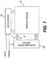
- FIG. 7 shows an overall structure of a display panel.
- a data signal and a timing signal are supplied to a data driver 20 and are supplied, as required, to the data lines 7 which are arranged such that each data line 7 corresponds to a pixel or a unit pixel.
- the data driver 20 is capable of outputting a pre-set voltage Vp.
- a gate and reset driver 22 controls the voltage of the selection line 8 and the reset line 9 in accordance with the timing.
- the selection lines 8 and the reset lines 9 are provided such that a pair of a selection line 8 and a reset line 9 is disposed corresponding to each row of the pixels or sub-pixels. In the above example, the voltage of the reset line 9 is controlled for each sub-pixel.
- a display region 24 is an area including the pixels arranged in a matrix.
- n-type transistors may be used. In this case, the polarities of the lines are appropriately changed. Further, while an organic EL element is adopted as a light emitting element in the example described above, other driven-by-current type light emitting elements may be used.
Landscapes
- Engineering & Computer Science (AREA)
- Physics & Mathematics (AREA)
- Computer Hardware Design (AREA)
- General Physics & Mathematics (AREA)
- Theoretical Computer Science (AREA)
- Electroluminescent Light Sources (AREA)
- Control Of Indicators Other Than Cathode Ray Tubes (AREA)
- Control Of El Displays (AREA)
Claims (2)
- Verfahren zum Liefern von Strom an ein organisches lichtemittierendes Element (1) in einem digital angesteuerten Anzeigepixel, wobei eine 3-Bit-Anzeige jedes Pixels unter Verwendung von vier Subrahmen durchgeführt wird, und ein Subrahmen (SFr) zum Rücksetzen zuerst gestartet wird und danach ein erster Subrahmen (SF0) für Bit 0, ein zweiter Subrahmen (SF1) für Bit 1 und ein dritter Subrahmen (SF2) für Bit 2 sequenziell gestartet werden, umfassend:(a) Bereitstellen einer Datenleitung (7), einer Auswahlleitung (8, 8-0, 8-1, 8-2), einer Energiequelle (10) und einer Rücksetzleitung (9);(b) Bereitstellen des Anzeigepixels mit:(i) einem Kopplungskondensator (6), der einen ersten Anschluss aufweist, der direkt mit der Datenleitung verbunden ist;(ii) einen Auswahltransistor (3), der den Drainanschluss mit einem zweiten Anschluss des Kopplungskondensators verbunden und den Gateanschluss mit der Auswahlleitung verbunden aufweist, wobei der Kopplungskondensator zwischen der Datenleitung und dem Drainanschluss des Auswahltransistors positioniert ist;(iii) einen Ansteuerungstransistor (2), der den Sourceanschluss mit der Energiequelle verbunden und den Gateanschluss mit dem Sourceanschluss des Auswahltransistors aufweist, wobei der Ansteuerungstransistor einen Strom von der Energiequelle in Übereinstimmung mit einem Gatepotenzial liefert;(iv) die Anode des organischen lichtemittierenden Elements, die mit dem Drainanschluss des Ansteuerungstransistors verbunden ist und Licht als Ergebnis des von der Stromquelle über den Ansteuerungstransistor gelieferten Stroms emittiert;(v) einen Rücksetztransistor (4), der den Sourceanschluss mit dem Drainanschluss des Ansteuerungstransistors verbunden aufweist, wobei der Drainanschluss mit dem Drainanschluss des Auswahltransistors verbunden ist und der Gateanschluss mit der Rücksetzleitung verbunden ist; und(vi) einen Speicherkondensator (5), der zwischen dem Gateanschluss des Ansteuerungstransistors und der Energiequelle zum Speichern des Gatepotenzials verbunden ist;(c) Bereitstellen einer Datenansteuerung (20) zum Bereitstellen eines Datensignals an die Datenleitung, wobei die Datenansteuerung der Datenleitung einen von drei festen Pegeln bereitstellt, wobei die drei festen Pegel eines von i) einem Datenpotenzial mit einem hohen Pegel, Vh, ii) einem Datenpotenzial mit einem niedrigen Pegel, Vl, und iii) einem Zwischenpotenzial, Vp, zwischen Vh und Vl sind;(d) Bereitstellen einer Gate- und Rücksetzansteuerung (22) zum Bereitstellen von jeweiligen Spannungen an die Auswahlleitung und die Rücksetzleitung; und(e) Durchführen die folgenden Schritte in Reihenfolge:(i) in einer Rücksetzperiode, Anlegen des Zwischenpotenzials Vp an die Datenleitung (7) und Anlegen eines Signals mit einem niedrigen Pegel an sowohl die Auswahlleitung (8) als auch die Rücksetzleitung, der den Auswahltransistor und den Rücksetztransistor EINschaltet, wobei eine Verbindung des Gateanschlusses und des Drainanschlusses des Ansteuerungstransistors (2) erreicht wird, wobei Strom im organischen lichtemittierenden Element (1) fließt, sodass ein Rücksetzpotenzial Vr, das durch das organische EL-Element (1) und den Ansteuerungstransistor (2) aufgeteilt wird, am Gateanschluss des Ansteuerungstransistors (2) erzeugt wird und in den Speicherkondensator (5) und den Kopplungskondensator (6) geschrieben wird;(ii) in einer nachfolgenden Schreibperiode:(iia) nachfolgend, wenn ein niedriges Datum geschrieben wird, das niedrige Datenpotenzial Vl an die Datenleitung (7) geliefert wird, die Auswahlleitung (8) auf einen niedrigen Pegel gesetzt wird, der den Auswahltransistor EINschaltet, die Rücksetzleitung auf einen hohen Pegel gesetzt wird, der den Rücksetztransistor AUSschaltet und das niedrige Datum über den Kopplungskondensator (6) in den Speicherkondensator (5) geschrieben wird, sodass eine Differenz zwischen dem Zwischenpotenzial, Vp, und dem Rücksetzpotenzial (Vr) während der Rücksetzperiode im Kopplungskondensator (6) gespeichert wird, und wenn das niedrige Potenzial (Vl) an die Datenleitung (7) angelegt ist, eine Gatespannung, Vg, des Ansteuerungstransistors (2), die Vg = Vr-(Vp-Vl) ist, erzeugt wird und der Ansteuerungstransistor (2) aufgrund des Gatepotenzials EINgeschaltet wird, das niedriger als das Rücksetzpotenzial ist, wobei der Kopplungskondensator (6) hinreichend größer als der Speicherkondensator (5) ist;(iib) wenn ein hohes Datum geschrieben wird, das hohe Potenzial Vh an die Datenleitung (7) geliefert wird, die Auswahlleitung (8) auf einen niedrigen Pegel gesetzt wird, der den Auswahltransistor EINschaltet, die Rücksetzleitung auf einen hohen Pegel gesetzt wird, der den Rücksetztransistor AUSschaltet, das Gatepotenzial, Vg, das Vg = Vr +(Vh-Vp) ist, über den Kopplungskondensator (6) in den Speicherkondensator (5) geschrieben wird, wodurch der Ansteuerungskondensator (2) AUSgeschaltet wird.
- Anzeigepixel, das ausgelegt ist, das Verfahren nach Anspruch 1 auszuführen.
Applications Claiming Priority (2)
| Application Number | Priority Date | Filing Date | Title |
|---|---|---|---|
| JP2008070549A JP5236324B2 (ja) | 2008-03-19 | 2008-03-19 | 表示パネル |
| PCT/US2009/001682 WO2009117092A1 (en) | 2008-03-19 | 2009-03-17 | Display panel |
Publications (2)
| Publication Number | Publication Date |
|---|---|
| EP2272059A1 EP2272059A1 (de) | 2011-01-12 |
| EP2272059B1 true EP2272059B1 (de) | 2019-06-12 |
Family
ID=40589714
Family Applications (1)
| Application Number | Title | Priority Date | Filing Date |
|---|---|---|---|
| EP09721681.6A Active EP2272059B1 (de) | 2008-03-19 | 2009-03-17 | Anzeigetafel |
Country Status (6)
| Country | Link |
|---|---|
| US (3) | US20110199359A1 (de) |
| EP (1) | EP2272059B1 (de) |
| JP (1) | JP5236324B2 (de) |
| KR (1) | KR20100126529A (de) |
| CN (1) | CN101978414B (de) |
| WO (1) | WO2009117092A1 (de) |
Families Citing this family (18)
| Publication number | Priority date | Publication date | Assignee | Title |
|---|---|---|---|---|
| WO2010143612A1 (ja) | 2009-06-12 | 2010-12-16 | シャープ株式会社 | 画素回路および表示装置 |
| WO2010143613A1 (ja) * | 2009-06-12 | 2010-12-16 | シャープ株式会社 | 画素回路および表示装置 |
| JP5399198B2 (ja) | 2009-10-08 | 2014-01-29 | グローバル・オーエルイーディー・テクノロジー・リミテッド・ライアビリティ・カンパニー | 画素回路および表示装置 |
| CN102646389B (zh) * | 2011-09-09 | 2014-07-23 | 京东方科技集团股份有限公司 | Oled面板及oled面板驱动方法 |
| JP6128738B2 (ja) * | 2012-02-28 | 2017-05-17 | キヤノン株式会社 | 画素回路及びその駆動方法 |
| KR101984196B1 (ko) * | 2012-12-13 | 2019-05-31 | 삼성디스플레이 주식회사 | 화소 회로 및 이를 포함하는 유기 발광 표시 장치 |
| CN103093723A (zh) * | 2013-03-04 | 2013-05-08 | 陈鑫 | 用于有机发光二极管的可进行阈值补偿的主动式像素驱动电路 |
| KR20150138527A (ko) | 2014-05-29 | 2015-12-10 | 삼성디스플레이 주식회사 | 화소 회로 및 이를 포함하는 전계발광 디스플레이 장치 |
| KR102583838B1 (ko) * | 2017-01-17 | 2023-10-05 | 삼성디스플레이 주식회사 | 화소 및 이를 이용한 유기전계발광 표시장치 |
| KR102575662B1 (ko) | 2017-02-06 | 2023-09-07 | 삼성디스플레이 주식회사 | 화소 및 이를 포함하는 표시 장치 |
| KR102660207B1 (ko) * | 2017-02-09 | 2024-04-25 | 삼성디스플레이 주식회사 | 화소 및 이를 포함하는 표시 장치 |
| KR102432347B1 (ko) * | 2018-02-28 | 2022-08-16 | 삼성디스플레이 주식회사 | 화소 회로 및 유기 발광 표시 장치 |
| KR102480426B1 (ko) * | 2018-03-15 | 2022-12-22 | 삼성디스플레이 주식회사 | 표시 장치 및 그 구동 방법 |
| KR102761331B1 (ko) * | 2019-10-24 | 2025-02-04 | 삼성디스플레이 주식회사 | 픽셀 회로 및 이를 포함하는 표시 장치 |
| CN111210767A (zh) * | 2020-03-05 | 2020-05-29 | 深圳市华星光电半导体显示技术有限公司 | 像素驱动电路及其驱动方法、显示面板 |
| CN111445858B (zh) * | 2020-04-20 | 2024-09-03 | 昆山国显光电有限公司 | 像素电路及其驱动方法、显示装置 |
| CN111768742B (zh) * | 2020-07-17 | 2021-06-01 | 武汉华星光电技术有限公司 | 像素驱动电路及显示面板 |
| JP2024093381A (ja) | 2022-12-27 | 2024-07-09 | セイコーエプソン株式会社 | 表示装置および電子機器 |
Family Cites Families (11)
| Publication number | Priority date | Publication date | Assignee | Title |
|---|---|---|---|---|
| JP3767877B2 (ja) * | 1997-09-29 | 2006-04-19 | 三菱化学株式会社 | アクティブマトリックス発光ダイオード画素構造およびその方法 |
| JP2002333870A (ja) | 2000-10-31 | 2002-11-22 | Matsushita Electric Ind Co Ltd | 液晶表示装置、el表示装置及びその駆動方法、並びに副画素の表示パターン評価方法 |
| JP4982014B2 (ja) * | 2001-06-21 | 2012-07-25 | 株式会社日立製作所 | 画像表示装置 |
| JP2003330422A (ja) | 2002-05-17 | 2003-11-19 | Hitachi Ltd | 画像表示装置 |
| JP4019843B2 (ja) * | 2002-07-31 | 2007-12-12 | セイコーエプソン株式会社 | 電子回路、電子回路の駆動方法、電気光学装置、電気光学装置の駆動方法及び電子機器 |
| JP3832415B2 (ja) * | 2002-10-11 | 2006-10-11 | ソニー株式会社 | アクティブマトリクス型表示装置 |
| JP4049037B2 (ja) * | 2003-06-30 | 2008-02-20 | ソニー株式会社 | 表示装置およびその駆動方法 |
| GB2411758A (en) * | 2004-03-04 | 2005-09-07 | Seiko Epson Corp | Pixel circuit |
| JP2005331891A (ja) | 2004-05-21 | 2005-12-02 | Eastman Kodak Co | 表示装置 |
| JP4834876B2 (ja) * | 2004-06-25 | 2011-12-14 | 京セラ株式会社 | 画像表示装置 |
| JP5308656B2 (ja) * | 2007-12-10 | 2013-10-09 | グローバル・オーエルイーディー・テクノロジー・リミテッド・ライアビリティ・カンパニー | 画素回路 |
-
2008
- 2008-03-19 JP JP2008070549A patent/JP5236324B2/ja active Active
-
2009
- 2009-03-17 EP EP09721681.6A patent/EP2272059B1/de active Active
- 2009-03-17 KR KR1020107023357A patent/KR20100126529A/ko not_active Ceased
- 2009-03-17 US US12/922,673 patent/US20110199359A1/en not_active Abandoned
- 2009-03-17 CN CN2009801095631A patent/CN101978414B/zh active Active
- 2009-03-17 WO PCT/US2009/001682 patent/WO2009117092A1/en not_active Ceased
-
2014
- 2014-02-20 US US14/184,879 patent/US9324249B2/en active Active
-
2016
- 2016-03-18 US US15/074,770 patent/US9552760B2/en active Active
Non-Patent Citations (1)
| Title |
|---|
| None * |
Also Published As
| Publication number | Publication date |
|---|---|
| KR20100126529A (ko) | 2010-12-01 |
| US9324249B2 (en) | 2016-04-26 |
| JP5236324B2 (ja) | 2013-07-17 |
| EP2272059A1 (de) | 2011-01-12 |
| WO2009117092A1 (en) | 2009-09-24 |
| US20110199359A1 (en) | 2011-08-18 |
| US20140176006A1 (en) | 2014-06-26 |
| CN101978414A (zh) | 2011-02-16 |
| JP2009223242A (ja) | 2009-10-01 |
| CN101978414B (zh) | 2013-01-30 |
| US9552760B2 (en) | 2017-01-24 |
| US20160203756A1 (en) | 2016-07-14 |
Similar Documents
| Publication | Publication Date | Title |
|---|---|---|
| EP2272059B1 (de) | Anzeigetafel | |
| CN110520922B (zh) | 显示驱动电路、方法、以及显示设备 | |
| CN1989539B (zh) | 显示驱动装置、显示装置及其驱动控制方法 | |
| EP2736039B1 (de) | Organische lichtemittierende Anzeigevorrichtung | |
| US8665186B2 (en) | Image display device and method of driving the same | |
| US20140168195A1 (en) | Electro-optic device and driving method thereof | |
| CN102246221B (zh) | 补偿像素晶体管的迁移率变化的显示装置 | |
| EP2439724B1 (de) | Anzeigevorrichtung und antriebsverfahren für die anzeigevorrichtung | |
| KR20190077689A (ko) | 유기 발광 다이오드 디스플레이 장치 | |
| WO2017115713A1 (ja) | 画素回路ならびに表示装置およびその駆動方法 | |
| KR102519364B1 (ko) | 게이트 구동부, 이를 포함하는 표시 장치 및 이를 이용한 표시 패널의 구동 방법 | |
| JP2006003752A (ja) | 表示装置及びその駆動制御方法 | |
| JP2005196116A (ja) | エレクトロルミネセンス表示装置及びその駆動方法 | |
| US10847094B2 (en) | Gate driver, organic light emitting display device and driving method thereof | |
| US8810488B2 (en) | Display device and method for driving the same | |
| JP2005031643A (ja) | 発光装置及び表示装置 | |
| US8456462B2 (en) | Display device | |
| KR20190074813A (ko) | 유기발광 다이오드 표시장치 및 그 구동 방법 | |
| JP5182382B2 (ja) | 表示装置 | |
| CN101488322B (zh) | 电光学装置、电光学装置的驱动方法以及电子机器 | |
| JP2010015187A (ja) | 表示装置及びその駆動制御方法 | |
| KR20080050878A (ko) | 유기발광다이오드 표시장치 및 그의 구동 방법 | |
| US20260120651A1 (en) | Data driver and display device including the same | |
| CN121838669A (zh) | 显示装置及其驱动方法 | |
| JP2011118406A (ja) | 表示装置 |
Legal Events
| Date | Code | Title | Description |
|---|---|---|---|
| PUAI | Public reference made under article 153(3) epc to a published international application that has entered the european phase |
Free format text: ORIGINAL CODE: 0009012 |
|
| 17P | Request for examination filed |
Effective date: 20100916 |
|
| AK | Designated contracting states |
Kind code of ref document: A1 Designated state(s): AT BE BG CH CY CZ DE DK EE ES FI FR GB GR HR HU IE IS IT LI LT LU LV MC MK MT NL NO PL PT RO SE SI SK TR |
|
| AX | Request for extension of the european patent |
Extension state: AL BA RS |
|
| RIN1 | Information on inventor provided before grant (corrected) |
Inventor name: KAWABE, KAZUYOSHI |
|
| DAX | Request for extension of the european patent (deleted) | ||
| RAP1 | Party data changed (applicant data changed or rights of an application transferred) |
Owner name: GLOBAL OLED TECHNOLOGY LLC |
|
| 17Q | First examination report despatched |
Effective date: 20160223 |
|
| STAA | Information on the status of an ep patent application or granted ep patent |
Free format text: STATUS: EXAMINATION IS IN PROGRESS |
|
| RAP1 | Party data changed (applicant data changed or rights of an application transferred) |
Owner name: GLOBAL OLED TECHNOLOGY LLC |
|
| GRAP | Despatch of communication of intention to grant a patent |
Free format text: ORIGINAL CODE: EPIDOSNIGR1 |
|
| STAA | Information on the status of an ep patent application or granted ep patent |
Free format text: STATUS: GRANT OF PATENT IS INTENDED |
|
| INTG | Intention to grant announced |
Effective date: 20190103 |
|
| GRAS | Grant fee paid |
Free format text: ORIGINAL CODE: EPIDOSNIGR3 |
|
| GRAA | (expected) grant |
Free format text: ORIGINAL CODE: 0009210 |
|
| STAA | Information on the status of an ep patent application or granted ep patent |
Free format text: STATUS: THE PATENT HAS BEEN GRANTED |
|
| AK | Designated contracting states |
Kind code of ref document: B1 Designated state(s): AT BE BG CH CY CZ DE DK EE ES FI FR GB GR HR HU IE IS IT LI LT LU LV MC MK MT NL NO PL PT RO SE SI SK TR |
|
| REG | Reference to a national code |
Ref country code: GB Ref legal event code: FG4D |
|
| REG | Reference to a national code |
Ref country code: CH Ref legal event code: EP |
|
| REG | Reference to a national code |
Ref country code: AT Ref legal event code: REF Ref document number: 1143597 Country of ref document: AT Kind code of ref document: T Effective date: 20190615 |
|
| REG | Reference to a national code |
Ref country code: DE Ref legal event code: R096 Ref document number: 602009058699 Country of ref document: DE |
|
| REG | Reference to a national code |
Ref country code: IE Ref legal event code: FG4D |
|
| REG | Reference to a national code |
Ref country code: NL Ref legal event code: MP Effective date: 20190612 |
|
| REG | Reference to a national code |
Ref country code: LT Ref legal event code: MG4D |
|
| PG25 | Lapsed in a contracting state [announced via postgrant information from national office to epo] |
Ref country code: ES Free format text: LAPSE BECAUSE OF FAILURE TO SUBMIT A TRANSLATION OF THE DESCRIPTION OR TO PAY THE FEE WITHIN THE PRESCRIBED TIME-LIMIT Effective date: 20190612 Ref country code: LT Free format text: LAPSE BECAUSE OF FAILURE TO SUBMIT A TRANSLATION OF THE DESCRIPTION OR TO PAY THE FEE WITHIN THE PRESCRIBED TIME-LIMIT Effective date: 20190612 Ref country code: FI Free format text: LAPSE BECAUSE OF FAILURE TO SUBMIT A TRANSLATION OF THE DESCRIPTION OR TO PAY THE FEE WITHIN THE PRESCRIBED TIME-LIMIT Effective date: 20190612 Ref country code: SE Free format text: LAPSE BECAUSE OF FAILURE TO SUBMIT A TRANSLATION OF THE DESCRIPTION OR TO PAY THE FEE WITHIN THE PRESCRIBED TIME-LIMIT Effective date: 20190612 Ref country code: NO Free format text: LAPSE BECAUSE OF FAILURE TO SUBMIT A TRANSLATION OF THE DESCRIPTION OR TO PAY THE FEE WITHIN THE PRESCRIBED TIME-LIMIT Effective date: 20190912 Ref country code: HR Free format text: LAPSE BECAUSE OF FAILURE TO SUBMIT A TRANSLATION OF THE DESCRIPTION OR TO PAY THE FEE WITHIN THE PRESCRIBED TIME-LIMIT Effective date: 20190612 |
|
| PG25 | Lapsed in a contracting state [announced via postgrant information from national office to epo] |
Ref country code: LV Free format text: LAPSE BECAUSE OF FAILURE TO SUBMIT A TRANSLATION OF THE DESCRIPTION OR TO PAY THE FEE WITHIN THE PRESCRIBED TIME-LIMIT Effective date: 20190612 Ref country code: BG Free format text: LAPSE BECAUSE OF FAILURE TO SUBMIT A TRANSLATION OF THE DESCRIPTION OR TO PAY THE FEE WITHIN THE PRESCRIBED TIME-LIMIT Effective date: 20190912 Ref country code: GR Free format text: LAPSE BECAUSE OF FAILURE TO SUBMIT A TRANSLATION OF THE DESCRIPTION OR TO PAY THE FEE WITHIN THE PRESCRIBED TIME-LIMIT Effective date: 20190913 |
|
| REG | Reference to a national code |
Ref country code: AT Ref legal event code: MK05 Ref document number: 1143597 Country of ref document: AT Kind code of ref document: T Effective date: 20190612 |
|
| PG25 | Lapsed in a contracting state [announced via postgrant information from national office to epo] |
Ref country code: PT Free format text: LAPSE BECAUSE OF FAILURE TO SUBMIT A TRANSLATION OF THE DESCRIPTION OR TO PAY THE FEE WITHIN THE PRESCRIBED TIME-LIMIT Effective date: 20191014 Ref country code: NL Free format text: LAPSE BECAUSE OF FAILURE TO SUBMIT A TRANSLATION OF THE DESCRIPTION OR TO PAY THE FEE WITHIN THE PRESCRIBED TIME-LIMIT Effective date: 20190612 Ref country code: AT Free format text: LAPSE BECAUSE OF FAILURE TO SUBMIT A TRANSLATION OF THE DESCRIPTION OR TO PAY THE FEE WITHIN THE PRESCRIBED TIME-LIMIT Effective date: 20190612 Ref country code: CZ Free format text: LAPSE BECAUSE OF FAILURE TO SUBMIT A TRANSLATION OF THE DESCRIPTION OR TO PAY THE FEE WITHIN THE PRESCRIBED TIME-LIMIT Effective date: 20190612 Ref country code: RO Free format text: LAPSE BECAUSE OF FAILURE TO SUBMIT A TRANSLATION OF THE DESCRIPTION OR TO PAY THE FEE WITHIN THE PRESCRIBED TIME-LIMIT Effective date: 20190612 Ref country code: EE Free format text: LAPSE BECAUSE OF FAILURE TO SUBMIT A TRANSLATION OF THE DESCRIPTION OR TO PAY THE FEE WITHIN THE PRESCRIBED TIME-LIMIT Effective date: 20190612 Ref country code: SK Free format text: LAPSE BECAUSE OF FAILURE TO SUBMIT A TRANSLATION OF THE DESCRIPTION OR TO PAY THE FEE WITHIN THE PRESCRIBED TIME-LIMIT Effective date: 20190612 |
|
| PG25 | Lapsed in a contracting state [announced via postgrant information from national office to epo] |
Ref country code: IT Free format text: LAPSE BECAUSE OF FAILURE TO SUBMIT A TRANSLATION OF THE DESCRIPTION OR TO PAY THE FEE WITHIN THE PRESCRIBED TIME-LIMIT Effective date: 20190612 Ref country code: IS Free format text: LAPSE BECAUSE OF FAILURE TO SUBMIT A TRANSLATION OF THE DESCRIPTION OR TO PAY THE FEE WITHIN THE PRESCRIBED TIME-LIMIT Effective date: 20191012 |
|
| REG | Reference to a national code |
Ref country code: DE Ref legal event code: R097 Ref document number: 602009058699 Country of ref document: DE |
|
| PG25 | Lapsed in a contracting state [announced via postgrant information from national office to epo] |
Ref country code: TR Free format text: LAPSE BECAUSE OF FAILURE TO SUBMIT A TRANSLATION OF THE DESCRIPTION OR TO PAY THE FEE WITHIN THE PRESCRIBED TIME-LIMIT Effective date: 20190612 |
|
| PLBE | No opposition filed within time limit |
Free format text: ORIGINAL CODE: 0009261 |
|
| STAA | Information on the status of an ep patent application or granted ep patent |
Free format text: STATUS: NO OPPOSITION FILED WITHIN TIME LIMIT |
|
| PG25 | Lapsed in a contracting state [announced via postgrant information from national office to epo] |
Ref country code: DK Free format text: LAPSE BECAUSE OF FAILURE TO SUBMIT A TRANSLATION OF THE DESCRIPTION OR TO PAY THE FEE WITHIN THE PRESCRIBED TIME-LIMIT Effective date: 20190612 Ref country code: PL Free format text: LAPSE BECAUSE OF FAILURE TO SUBMIT A TRANSLATION OF THE DESCRIPTION OR TO PAY THE FEE WITHIN THE PRESCRIBED TIME-LIMIT Effective date: 20190612 |
|
| 26N | No opposition filed |
Effective date: 20200313 |
|
| PG25 | Lapsed in a contracting state [announced via postgrant information from national office to epo] |
Ref country code: SI Free format text: LAPSE BECAUSE OF FAILURE TO SUBMIT A TRANSLATION OF THE DESCRIPTION OR TO PAY THE FEE WITHIN THE PRESCRIBED TIME-LIMIT Effective date: 20190612 Ref country code: IS Free format text: LAPSE BECAUSE OF FAILURE TO SUBMIT A TRANSLATION OF THE DESCRIPTION OR TO PAY THE FEE WITHIN THE PRESCRIBED TIME-LIMIT Effective date: 20200224 |
|
| PG2D | Information on lapse in contracting state deleted |
Ref country code: IS |
|
| PG25 | Lapsed in a contracting state [announced via postgrant information from national office to epo] |
Ref country code: IS Free format text: LAPSE BECAUSE OF FAILURE TO SUBMIT A TRANSLATION OF THE DESCRIPTION OR TO PAY THE FEE WITHIN THE PRESCRIBED TIME-LIMIT Effective date: 20191112 |
|
| PG25 | Lapsed in a contracting state [announced via postgrant information from national office to epo] |
Ref country code: MC Free format text: LAPSE BECAUSE OF FAILURE TO SUBMIT A TRANSLATION OF THE DESCRIPTION OR TO PAY THE FEE WITHIN THE PRESCRIBED TIME-LIMIT Effective date: 20190612 |
|
| REG | Reference to a national code |
Ref country code: CH Ref legal event code: PL |
|
| REG | Reference to a national code |
Ref country code: BE Ref legal event code: MM Effective date: 20200331 |
|
| PG25 | Lapsed in a contracting state [announced via postgrant information from national office to epo] |
Ref country code: LU Free format text: LAPSE BECAUSE OF NON-PAYMENT OF DUE FEES Effective date: 20200317 |
|
| PG25 | Lapsed in a contracting state [announced via postgrant information from national office to epo] |
Ref country code: CH Free format text: LAPSE BECAUSE OF NON-PAYMENT OF DUE FEES Effective date: 20200331 Ref country code: LI Free format text: LAPSE BECAUSE OF NON-PAYMENT OF DUE FEES Effective date: 20200331 Ref country code: IE Free format text: LAPSE BECAUSE OF NON-PAYMENT OF DUE FEES Effective date: 20200317 |
|
| PG25 | Lapsed in a contracting state [announced via postgrant information from national office to epo] |
Ref country code: BE Free format text: LAPSE BECAUSE OF NON-PAYMENT OF DUE FEES Effective date: 20200331 |
|
| PG25 | Lapsed in a contracting state [announced via postgrant information from national office to epo] |
Ref country code: MT Free format text: LAPSE BECAUSE OF FAILURE TO SUBMIT A TRANSLATION OF THE DESCRIPTION OR TO PAY THE FEE WITHIN THE PRESCRIBED TIME-LIMIT Effective date: 20190612 Ref country code: CY Free format text: LAPSE BECAUSE OF FAILURE TO SUBMIT A TRANSLATION OF THE DESCRIPTION OR TO PAY THE FEE WITHIN THE PRESCRIBED TIME-LIMIT Effective date: 20190612 |
|
| PG25 | Lapsed in a contracting state [announced via postgrant information from national office to epo] |
Ref country code: MK Free format text: LAPSE BECAUSE OF FAILURE TO SUBMIT A TRANSLATION OF THE DESCRIPTION OR TO PAY THE FEE WITHIN THE PRESCRIBED TIME-LIMIT Effective date: 20190612 |
|
| PGFP | Annual fee paid to national office [announced via postgrant information from national office to epo] |
Ref country code: GB Payment date: 20260324 Year of fee payment: 18 |
|
| PGFP | Annual fee paid to national office [announced via postgrant information from national office to epo] |
Ref country code: DE Payment date: 20260319 Year of fee payment: 18 |
|
| PGFP | Annual fee paid to national office [announced via postgrant information from national office to epo] |
Ref country code: FR Payment date: 20260320 Year of fee payment: 18 |