EP2273575B1 - Weisse LED-Lichtquelle - Google Patents
Weisse LED-Lichtquelle Download PDFInfo
- Publication number
- EP2273575B1 EP2273575B1 EP10185808.2A EP10185808A EP2273575B1 EP 2273575 B1 EP2273575 B1 EP 2273575B1 EP 10185808 A EP10185808 A EP 10185808A EP 2273575 B1 EP2273575 B1 EP 2273575B1
- Authority
- EP
- European Patent Office
- Prior art keywords
- led
- leds
- color conversion
- wavelength
- blue
- Prior art date
- Legal status (The legal status is an assumption and is not a legal conclusion. Google has not performed a legal analysis and makes no representation as to the accuracy of the status listed.)
- Expired - Lifetime
Links
Images
Classifications
-
- H—ELECTRICITY
- H10—SEMICONDUCTOR DEVICES; ELECTRIC SOLID-STATE DEVICES NOT OTHERWISE PROVIDED FOR
- H10H—INORGANIC LIGHT-EMITTING SEMICONDUCTOR DEVICES HAVING POTENTIAL BARRIERS
- H10H20/00—Individual inorganic light-emitting semiconductor devices having potential barriers, e.g. light-emitting diodes [LED]
- H10H20/80—Constructional details
- H10H20/85—Packages
- H10H20/851—Wavelength conversion means
-
- H—ELECTRICITY
- H10—SEMICONDUCTOR DEVICES; ELECTRIC SOLID-STATE DEVICES NOT OTHERWISE PROVIDED FOR
- H10H—INORGANIC LIGHT-EMITTING SEMICONDUCTOR DEVICES HAVING POTENTIAL BARRIERS
- H10H20/00—Individual inorganic light-emitting semiconductor devices having potential barriers, e.g. light-emitting diodes [LED]
- H10H20/01—Manufacture or treatment
- H10H20/036—Manufacture or treatment of packages
- H10H20/0361—Manufacture or treatment of packages of wavelength conversion means
Definitions
- the invention relates to a set of light-emitting diodes (LEDs), which emit white light with a predetermined color temperature.
- LEDs light-emitting diodes
- white LEDs in which a blue light-emitting LED, hereinafter referred to as “blue LED”, coated with a conversion layer that absorbs blue light and emits light of longer wavelength, are coated.
- blue LED coated with a conversion layer that absorbs blue light and emits light of longer wavelength, are coated.
- the invention further relates to an LED module having such a set of white LEDs.
- the color conversion layer typically consists of inorganic or organic color conversion pigments which are distributed in an organic plastic layer.
- the layer thickness (and its shape) must be precisely defined during the production process.
- WO 03/038902 A discloses a method of fabricating a white LED having a given color temperature, comprising a plurality of blue LED chips, wherein the exact wavelength of the LED chips is determined, the LED chips having a conversion layer that absorbs blue light and emits light of a longer wavelength, are coated, wherein the color conversion agent is applied in a dependent of the determined wavelength amount.
- DE 10135306 A1 discloses a white LED light source having a plurality of blue LED chips having a wavelength of 455 nm each coated with a conversion layer of a color conversion agent which absorbs blue light and emits light of a larger wavelength, with a different amount of color conversion agent depending on the spectrum present is applied to the respective LED chip, so that the color temperature of the modulated light of the LED light source is 6000K.
- the excitability of color conversion agents is typically highly dependent on the wavelength of the exciting LEDs. Especially with long-wave blue LEDs, a wavelength tolerance of only a few nanometers already leads to significantly different emission intensities in the current color conversion agents. In the case of UV LEDs, this would lead predominantly to a fluctuation in intensity, in the case of blue LEDs, moreover, to a color shift, since in this case the white light is composed of the blue LED emission and the emission of the color conversion agent.
- a typical selection class has a wavelength tolerance of more than 5 nm. Even with very defined application of the color conversion agent (with negligible tolerance), this results in a tolerance of the color temperature of white LEDs of more than ⁇ 300 K. This is already too high for many applications. It therefore corresponds to the prior art that the market demand for narrower specified white LEDs is realized by selection process.
- This object is achieved in that the exact wavelength of the LED is determined prior to applying the color conversion agent and then the color conversion agent is applied over this LED in a dependent of the determined wavelength concentration.
- the manufacturing process can be roughly described as follows:
- LEDs are made in wafers. It corresponds to the state of the art that the individual LEDs on a wafer are individually measured with regard to brightness and wavelength ( ⁇ ⁇ 1 nm) (wafer mapping, see product specification of the machine manufacturer, for example ASM). These data are subsequently used to select the LEDs after separating into different classes. Alternatively, the optical data of the LEDs may be measured individually before application of color conversion by spectrometer (or chroma meter).
- the information of the wafer mapping is used to selectively apply to each LED a specific amount of color conversion agent.
- the amount of color conversion agent is selectively adjusted by appropriate choice of concentration (in diluted systems) to the respective LED.
- the LEDs are grouped together, e.g. each in the range of 1 nm.
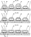
- Fig. 1 a not inventive example of LED's with different amount of binder in which the color conversion phosphorus pigment is
- Fig. 2 an exemplary embodiment of LED's with equal amounts of binder, in which the color conversion phosphorus pigment is located with different concentration
- Fig. 3 shows a modification of the embodiment according to Fig. 2 ,
- Example not according to the invention color conversion phosphorus pigment dispersed in organic binder with constant concentration - application by means of a dispenser
- a circuit board 1 is shown on which there are four LED dices 2a, 2b, 2c, 2d. These LED dices 2 a, 2 b, 2 c, 2 d are applied in flip-chip technology, ie the terminals 3 are located on the underside and are connected to the board 1 with contact bumps 4. Above each LED dice 2a, 2b, 2c, 2d is a drop of a binder 5 containing the color conversion phosphorus pigment.
- the amount of drops is adjusted to the wavelength of the LED dices 2a, 2b, 2c, 2d.
- the drop quantity is increased for long-wavelength LED dices 2b, 2c, while this is reduced for short-wave LED dices 2d. Since the viscosity and thixotropy of the paste depends on the concentration of the color conversion pigment, a change in the drop shape can also be achieved (at a volumetric dosage).
- the concentration of phosphorus pigments in binder 6 in the matrix is adapted. This is preferably achieved by using multiple dispensing or stamping containers with different concentrations of the phosphor pigments. The different concentration is in Fig. 2 indicated by hatching at different distances
- a printing operation can be connected to achieve a flat and defined shape of the color conversion medium (see Fig. 3 ).
- a mask is placed over the LED array, in the recesses of which the color conversion medium is applied by means of a dispenser. Finally, the material protruding over the mask is removed by means of a doctor blade.
- a variation of the phosphorus pigment in the organic matrix between 10 and 30 mass% on dices with a wavelength variation between 460 and 475 nm produces white light with a color temperature of 6500 ⁇ 200K.
- the LEDs mounted in this way are individually measured with respect to the wavelength in a mapping process and with this data the dispenser is programmed.
- the individual LEDs can subsequently be divided along dividing lines 7 and processed into LED light sources or also be used as an LED module.
- Inkjet Printing is a refinement of dispensing methods I-II. This requires fine-grained pigments (in the range of at most a few micrometers in diameter).
- ZnS: Mn some materials which are suitable for the color conversion of the light emitted by LEDs and which can be deposited by means of gas-phase methods.
- the selective color conversion is achieved in this method by defined adjustment of the applied amount of the color conversion material. This can be done in the simplest case by attaching a mask (typical photomask), which is specially adapted to the coated LED wafer (according to the wafer mapping data). In this way, a LED with the highest wavelength (which normally causes best excitability) is completely coated, while with LEDs with a shorter wavelength, only parts of the surface are coated.
- a mask typically photomask
- the coated LED is trimmed in such a way that a laser ablates color conversion material from the surface of the LEDs in a defined manner (laser ablation) so that the desired color is defined by the defined color Amount of leftover color conversion material is achieved regardless of the wavelength of the LED.
Landscapes
- Led Device Packages (AREA)
- Ink Jet (AREA)
- Ink Jet Recording Methods And Recording Media Thereof (AREA)
Description
- Die Erfindung betrifft einen Satz an Lichtemittierenden Dioden (LEDs), die weißes Licht mit vorgegebener Farbtemperatur aussenden. Im Folgenden werden als "weiße LED" bezeichnet, bei denen eine blaues Licht aussendende LED, im Folgenden als "blaue LED" bezeichnet, mit einer Konversionsschicht, die blaues Licht absorbiert und Licht größerer Wellenlänge emittiert, beschichtet werden. Bei einer blauen LED wird ein Teil der blauen Emission in einen anderen Wellenlängenbereich konvertiert, so dass die Summe der emittierten Lichtkomponenten weißes Licht ergibt. Die Erfindung betrifft weiters ein LED-Modul, der einen solchen Satz an weißen LEDs aufweist.
- Die Farbkonversionsschicht besteht typisch aus anorganischen oder organischen Farbkonversionspigmenten, welche in einer organischen Kunststoffschicht verteilt sind.
- Im Hinblick auf eine reproduzierbare Herstellung von weißen LEDs innerhalb enger Toleranzen des resultierenden Farbortes muss beim Herstellungsprozess neben der Konzentration der Pigmente auch die Schichtdicke (und deren Form) exakt definiert sein.
- Im Stand der Technik sind diesbezüglich verschiedene Prozesse bekannt:
- 1) Das Farbkonversionsmedium füllt den Reflektor-Cup, in welchen die LED eingesetzt wird, aus
(JP 8335719 A
JP 8335720 A - 2) Das Farbkonversionsmedium wird in Tropfenform über dem LED-Chip aufgebracht (mit transparentem Spacer:
-
US 5959316 A -. -
JP 10190065 A
-
- 3) Das Farbkonversionsmedium wird in die Klebeschicht zwischen der LED und einer Linse eingebracht (
US 6590235 B --.); - 4) Das Farbkonversionsmedium wird in Schichtform definiert hergestellt und auf der LED befestigt (
EP 1081771 A --.); - 5) Die Farbkonversionsschicht wird direkt auf den LED-Chip gedruckt (
JP 2001244507 A -
WO 03/038902 A -
DE 10135306 A1 offenbart eine weiße LED-Lichtquelle mit mehreren blauen LED-Chips die eine Wellenlänge von 455 nm aufweisen, die jeweils mit einer Konversionsschicht aus einem Farbkonversionsmittel beschichtet sind, die blaues Licht absorbiert und Licht größerer Wellenlänge emittiert, wobei je nach vorliegendem Spektrum eine andere Menge Farbkonversionsmittel auf den jeweiligen LED-Chip aufgebracht wird, so dass die Farbtemperatur des modulierten Lichts der LED-Lichtquelle bei 6000K liegt. - Diese Methoden erfüllen die Anforderungen für viele Anwendungen, speziell für Beleuchtung, unzureichend. Die Herstellungsmethode und deren Toleranzen sind wesentliche Gründe für die Abweichungen. Ein weiterer Grund ist der folgende:
- Die Anregbarkeit der Farbkonversionsmittel hängt typischerweise stark von der Wellenlänge der anregenden LEDs ab. Speziell bei langwelligen blauen LEDs führt eine WeDenlängentoleranz von nur einigen Nanometern bereits zu signifikant unterschiedlichen Emissionsintensitäten bei den derzeitigen Farbkonversionsmitteln. Im Falle von UV-LEDs würde dies vorwiegend zu einer Intensitätsschwankung führen, im Falle von blauen LEDs darüber hinaus zu einer Farbverschiebung, da sich in diesem Fall das weiße Licht aus der blauen LED-Emission und der Emission des Farbkonversionsmittels zusammensetzt.
- Da LEDs gemäß dem Stand der Produktionstechnik eine relativ breite Wellenlängenverteilung aufweisen, weist eine typische Selektionsklasse eine Wellenlängentoleranz von mehr als 5 nm auf. Selbst bei sehr definierter Aufbringung der Farbkonversionsmittel (mit vernachlässigbarer Toleranz) resultiert hieraus eine Toleranz der Farbtemperatur weißer LEDs von mehr als ± 300 K. Dies ist für viele Anwendungen bereits zu hoch. Es entspricht daher dem Stand der Technik, dass die Marktforderung nach enger spezifizierten weißen LEDs durch Selektionsverfahren realisiert wird.
- Es ist Aufgabe der Erfindung, weiße LEDs zu schaffen, welche geringere Toleranz der Farbtemperatur haben, als es dem Stand der Technik entspricht. Weiters soll ein weißes LED-Modul geschaffen werden, die eine geringere Schwankungsbreite der Farbtemperatur hat, die insbesondere also über der gesamten Emissionsfläche eine nahezu konstante Farbtemperatur hat.
- Diese Aufgabe wird erfindungsgemäß dadurch gelöst, dass die genaue Wellenlänge der LED vor dem Aufbringen des Farbkonversionsmittels bestimmt wird und sodann das Farbkonversionsmittel über dieser LED in einer von der ermittelten Wellenlänge abhängigen Konzentration aufgebracht wird.
- Im Gegensatz zum Stand der Technik ist durch die Erfindung eine Herstellung von weißen LEDs mit definierter Farbtemperatur und definierter Toleranz möglich, ohne dass ein weiteres Selektionsverfahren notwenig wäre.
- Der Herstellungsprozess kann grob folgendermaßen beschrieben werden:
- LEDs werden in Wafern hergestellt. Es entspricht dem Stand der Technik, dass die einzelnen LEDs auf einem Wafer einzeln bezüglich Helligkeit und Wellenlänge (Δλ < 1nm) vermessen werden (Wafer Mapping, siehe Produktspezifikation der Maschinenhersteller, z.B. ASM). Diese Daten werden in weiterer Folge dazu verwendet, die LEDs nach dem Vereinzeln in verschiedene Klassen zu selektieren. Alternativ können die optischen Daten der LEDs einzeln vor der Aufbringung der Farbkonversion mittels Spektrometer (oder Chromameter) gemessen werden.
- In gegenständlicher Erfindung wird die Information des Wafer Mappings dazu benutzt, um auf jede LED selektiv eine spezielle Menge Farbkonversionsmittel aufzubringen. Die Menge an Farbkonversionsmittel ist hierbei selektiv durch entsprechende Wahl der Konzentration (bei verdünnten Systemen) auf die jeweilige LED abgestimmt.
- Bei der Aufbringung des Farbkonversionsmittels gibt es folgende Möglichkeiten:
- Selektives Dispensen oder Stempeln
- Selektives Inkjet Printing
- Selektives Verdampfen durch Masken
- Selektives nachträgliches Einstellen der Dicke und Form der Schicht des Farbkonversionsmittels (z.B. durch Laser wie beim Widerstandstrimmen).
- Zur Vereinfachung werden die LEDs in Gruppen zusammengezogen, z.B. jeweils im Bereich von 1 nm.
- Anhand der Zeichnung wird die Erfindung näher erläutert. Es zeigt:
Fig. 1 ein nicht erfindungsgemäßes Beispiel von LED's mit unterschiedlicher Menge von Binder, in dem sich das Farbkonversionsphosphorpigment befindet;Fig. 2 ein erfindungsgemäßes Ausfuhrungsbeispiel von LED's mit gleichen Mengen von Binder, in dem sich das Farbkonversionsphosphorpigment mit unterschiedlicher Konzentration befindet; undFig. 3 zeigt eine Abwandlung der Ausführungsform gemäßFig. 2 . - Es folgen nun fünf Beispiele:
- In
Fig. 1 ist eine Platine 1 gezeigt, auf der sich vier LED-Dices 2a, 2b, 2c, 2d befinden. Diese LED-Dices 2a, 2b, 2c, 2d sind in Flip-Chip-Technologie aufgebracht, d.h. die Anschlüsse 3 befinden sich auf der Unterseite und sind mit Kontakt-Bumps 4 mit der Platine 1 verbunden. Über jedem LED-Dice 2a, 2b, 2c, 2d befindet sich ein Tropfen eines Binders 5, der das Farbkonversionsphosphorpigment enthält. - Man stimmt die Tropfenmenge auf die Wellenlänge der LED-Dices 2a, 2b, 2c, 2d ab. Gemäß der ermittelten Wellenlänge der einzelnen LED-Dices 2a, 2b, 2c, 2d wird die Tropfenmenge erhöht für langwellige LED-Dices 2b, 2c, während diese für kurzwellige LED-Dices 2d reduziert wird. Da die Viskosität und Thixotropie der Paste von der Konzentration des Farbkonversionspigmentes abhängt, kann auch eine Veränderung der Tropfenform erzielt werden (bei einer volumetrischen Dosierung).
- Mit diesen Methoden konnte durch eine Variation des Dispens-Volumens zwischen 0,02 und 0,03 cm3 auf Dices, deren Wellenlängen zwischen 460 und 475 nm variierten, weißes Licht mit einer Farbtemperatur von 6500 ± 300 K realisiert werden.
- Gemäß der Wellenlänge der einzelnen LED-Dices 2a, 2b, 2c, 2d (siehe
Fig. 2 ) wird die Konzentration der Phosphorpigmente im Binder 6 in der Matrix adaptiert. Dies wird bevorzugt durch das Verwenden von mehreren Dispens- oder Stempelbehältern mit unterschiedlichen Konzentrationen der Phosphorpigmente erreicht Die unterschiedliche Konzentration ist inFig. 2 durch Schraffen mit unterschiedlichem Abstand angedeutet - Optional kann nach dem Dispens- oder Stempelvorgang ein Druckvorgang angeschlossen werden, um eine ebene und definierte Form des Farbkonversionsmediums zu erreichen (siehe
Fig. 3 ). Hiezu wird über der LED-Anordnung eine Maske aufgelegt, in deren Ausnehmungen das Farbkonversionsmedium mittels Dispenser aufgebracht wird. Abschließend wird mittels eines Rakels das über die Maske herausstehende Material entfernt. - Mit diesen Methoden werden durch eine Variation des Phosphorpigmentes in der organischen Matrix zwischen 10 und 30 Masse-% auf Dices mit einer Wellenlängenvariation zwischen 460 und 475 nm weißes Licht mit einer Farbtemperatur von 6500±200K realisiert.
- Die Methoden I und II werden bevorzugt für LED-Dices eingesetzt, die Face Down (Elektrode nach unten) auf Trägermaterialien (Halbleiterträger oder printed circuit board = PCB) angeordnet sind, da es bei einer Face Up Montage schwierig ist, die Elektroden frei von der Farbkonversionspaste zu halten. Die derart montierten LEDs werden in einem Mapping-Verfahren einzeln bezüglich der Wellenlänge vermessen und mit diesen Daten wird der Dispenser programmiert. Die einzelnen LEDs können nachfolgend entlang von Trennlinien 7 geteilt und zu LED-Lichtquellen verarbeitet werden bzw. auch als LED-Modul eingesetzt werden.
- Das Inkjet Printing stellt eine Verfeinerung der Dispensmethoden I-II dar. Hiezu sind feinkörnige Pigmente (im Bereich von höchstens einigen Mikrometern Durchmesser) notwendig.
- Die individuelle Einstellung der Farbkonversion pro LED kann derart mittels der Anzahl der gesetzten Inkjettropfen (=volumetrisch) oder der Konzentration durch Einsatz verschiedener Inkjet-Tinten (aus verschiedenen Kartuschen) oder deren Kombination erfolgen.
- Gemäß dem Stand der Technik sind einige Materialien (ZnS:Mn) bekannt, die sich zur Farbkonversion des von LEDs ausgesandten Lichts eignen und welche mittels Gasphasenmethoden abgeschieden werden können.
- Einer der Vorteile dieser Methoden ist, dass die Elektroden der LEDs selektiv abgedeckt werden können und daher diese Methode auch für Face Up montierte LEDs sehr gut geeignet ist. (Man kann die Kontaktflächen einfach abdecken.)
- Die selektive Farbkonversion wird bei dieser Methode durch definierte Einstellung der aufgebrachten Menge des Farbkonversionsmaterials erreicht. Dies kann im einfachsten Fall durch Anbringen einer Maske (typisch Photomaske), die speziell auf den zu beschichteten LED Wafer (gemäß den Wafer Mapping Daten) abgestimmt ist, erfolgen. Derart wird eine LED mit der höchsten Wellenlänge (was normalerweise beste Anregbarkeit bewirkt) vollständig beschichtet, während bei LEDs mit geringerer Wellenlänge nur Teile der Oberfläche beschichtet werden.
- Das Einstellen der Farbkonversion bei vollflächig aufgebrachten Schichten (gleicher Konzentration) kann auch nachträglich erfolgen. Hiezu kann ein Verfahren angewandt werden, welches in der Halbleiter- und Drucktechnik eingesetzt wird, um z.B. Widerstände definiert abzugleichen. Hiezu wird die beschichtete LED derart getrimmt, dass ein Laser Farbkonversionsmaterial vom der Oberfläche der LEDs definiert abträgt (Laserablation), sodass die gewünschte Farbe durch die definierte Menge an übrig gelassenem Farbkonversionsmaterial unabhängig von der Wellenlänge der LED erreicht wird.
Claims (4)
- Satz an weißen LEDs, jeweils mit einer blauen LED (2a, 2b, 2c, 2d), die mit einer Konversionsschicht aus einem Farbkonversionsmittel beschichtet ist, die blaues Licht absorbiert und Licht größerer Wellenlänge emittiert, wobei die blauen LEDs eine Wellenlänge zwischen 460 und 475nm aufweisen; wobei die Konzentration der Konversionsschicht über jeder blauen LED von der genauen Wellenlänge der jeweiligen blauen LED abhängt, wobei die Konzentration von Phosphorpigmenten in einer organischen Matrix (6) der Konversionsschicht zwischen 10 und 30 Masseprozent variiert, und
wobei die Gesamt-Emissionsflächen der weißen LEDs eine Farbtemperatur von 6500 ±200K aufweisen. - Satz an weißen LEDs nach Anspruch 1,
dadurch gekennzeichnet, daß die Konversionsschicht aus anorganischen oder organischen Farbkonversionspigmenten besteht, welche in einer organischen Kunststoffschicht (6) verteilt sind. - LED-Modul, das einen Satz an weißen LEDs nach einem der vorhergehenden Ansprüchen aufweist, wobei die LED-Dices (2a, 2b, 2c, 2d) der blauen LEDs Face Down auf einem Trägermaterial (1) angeordnet sind.
- LED-Modul nach Anspruch 3,
dadurch gekennzeichnet,
daß das Trägermaterial (1) ein Halbleiterträger oder ein PCB ist.
Applications Claiming Priority (3)
| Application Number | Priority Date | Filing Date | Title |
|---|---|---|---|
| AT0094803A AT412928B (de) | 2003-06-18 | 2003-06-18 | Verfahren zur herstellung einer weissen led sowie weisse led-lichtquelle |
| EP04741759.7A EP1820220B1 (de) | 2003-06-18 | 2004-06-09 | Verfahren zur herstellung weisser leuchtdioden |
| PCT/EP2004/051065 WO2004112152A2 (de) | 2003-06-18 | 2004-06-09 | Verfahren zur herstellung weisser led’s sowie weisse led-lichtquelle |
Related Parent Applications (3)
| Application Number | Title | Priority Date | Filing Date |
|---|---|---|---|
| EP04741759.7 Division | 2004-06-09 | ||
| EP04741759.7A Division EP1820220B1 (de) | 2003-06-18 | 2004-06-09 | Verfahren zur herstellung weisser leuchtdioden |
| EP04741759.7A Division-Into EP1820220B1 (de) | 2003-06-18 | 2004-06-09 | Verfahren zur herstellung weisser leuchtdioden |
Publications (3)
| Publication Number | Publication Date |
|---|---|
| EP2273575A2 EP2273575A2 (de) | 2011-01-12 |
| EP2273575A3 EP2273575A3 (de) | 2015-02-25 |
| EP2273575B1 true EP2273575B1 (de) | 2019-08-07 |
Family
ID=33545802
Family Applications (2)
| Application Number | Title | Priority Date | Filing Date |
|---|---|---|---|
| EP04741759.7A Expired - Lifetime EP1820220B1 (de) | 2003-06-18 | 2004-06-09 | Verfahren zur herstellung weisser leuchtdioden |
| EP10185808.2A Expired - Lifetime EP2273575B1 (de) | 2003-06-18 | 2004-06-09 | Weisse LED-Lichtquelle |
Family Applications Before (1)
| Application Number | Title | Priority Date | Filing Date |
|---|---|---|---|
| EP04741759.7A Expired - Lifetime EP1820220B1 (de) | 2003-06-18 | 2004-06-09 | Verfahren zur herstellung weisser leuchtdioden |
Country Status (5)
| Country | Link |
|---|---|
| US (2) | US8227273B2 (de) |
| EP (2) | EP1820220B1 (de) |
| AT (1) | AT412928B (de) |
| CA (1) | CA2553912C (de) |
| WO (1) | WO2004112152A2 (de) |
Families Citing this family (21)
| Publication number | Priority date | Publication date | Assignee | Title |
|---|---|---|---|---|
| US7928455B2 (en) * | 2002-07-15 | 2011-04-19 | Epistar Corporation | Semiconductor light-emitting device and method for forming the same |
| JP2007188976A (ja) * | 2006-01-11 | 2007-07-26 | Shinko Electric Ind Co Ltd | 発光装置の製造方法 |
| US8232563B2 (en) * | 2007-06-14 | 2012-07-31 | Epistar Corporation | Light-emitting device |
| DE102008014121A1 (de) * | 2007-12-20 | 2009-06-25 | Osram Opto Semiconductors Gmbh | Verfahren zur Herstellung von Halbleiterchips und Halbleiterchip |
| US8896317B2 (en) | 2008-02-15 | 2014-11-25 | Nxp B.V. | Lighting unit with compensation for output frequency, and method for determining output frequency |
| WO2009118985A2 (en) * | 2008-03-25 | 2009-10-01 | Kabushiki Kaisha Toshiba | Light emitting device, and method and apparatus for manufacturing same |
| JP2010103349A (ja) * | 2008-10-24 | 2010-05-06 | Toshiba Corp | 発光装置の製造方法 |
| KR101562374B1 (ko) * | 2008-11-03 | 2015-10-23 | 서울바이오시스 주식회사 | 교류용 발광 소자 모듈 |
| JP2010103522A (ja) * | 2008-10-21 | 2010-05-06 | Seoul Opto Devices Co Ltd | 遅延蛍光体を備える交流駆動型の発光素子及び発光素子モジュール |
| US8716038B2 (en) * | 2010-03-02 | 2014-05-06 | Micron Technology, Inc. | Microelectronic workpiece processing systems and associated methods of color correction |
| DE102011003608A1 (de) * | 2010-08-20 | 2012-02-23 | Tridonic Gmbh & Co. Kg | Gehäustes LED-Modul |
| MY152737A (en) * | 2010-08-24 | 2014-11-28 | Silq Malaysia Sdn Bhd | Methodology of forming optical lens for semiconductor light emitting device |
| EP2503605B1 (de) * | 2010-09-15 | 2016-07-20 | Lightizer Korea Co., Ltd | Lichtemittierende diode und verfahren zu ihrer herstellung |
| TW201340422A (zh) * | 2012-03-30 | 2013-10-01 | Hon Hai Prec Ind Co Ltd | 發光二極體焊接方法 |
| US9147816B2 (en) * | 2012-08-24 | 2015-09-29 | Luminus Devices, Inc. | Wavelength converting material deposition methods and associated articles |
| US20140268731A1 (en) | 2013-03-15 | 2014-09-18 | Lighting Science Group Corpporation | Low bay lighting system and associated methods |
| JP2014064046A (ja) * | 2014-01-17 | 2014-04-10 | Toshiba Corp | 発光装置の製造方法 |
| CN105870310A (zh) * | 2016-04-22 | 2016-08-17 | 江门市迪司利光电股份有限公司 | 一种照明范围大色温均匀的led封装结构 |
| CN105810806A (zh) * | 2016-04-22 | 2016-07-27 | 江门市迪司利光电股份有限公司 | 一种色温均匀散热性良好的led封装结构 |
| CN109952651B (zh) * | 2016-11-17 | 2023-10-10 | 昕诺飞控股有限公司 | 具有uv led的照明装置 |
| CN109148429B (zh) * | 2018-08-28 | 2020-09-22 | 开发晶照明(厦门)有限公司 | 发光二极管封装结构 |
Citations (1)
| Publication number | Priority date | Publication date | Assignee | Title |
|---|---|---|---|---|
| EP1296376A2 (de) * | 2001-09-25 | 2003-03-26 | Patent-Treuhand-Gesellschaft für elektrische Glühlampen mbH | Beleuchtungseinheit mit mindestens einer LED als Lichtquelle |
Family Cites Families (19)
| Publication number | Priority date | Publication date | Assignee | Title |
|---|---|---|---|---|
| JPH08335720A (ja) * | 1995-06-08 | 1996-12-17 | Nichia Chem Ind Ltd | 窒化物半導体発光ダイオード |
| JP3271645B2 (ja) * | 1995-06-08 | 2002-04-02 | 日亜化学工業株式会社 | 窒化物半導体発光ダイオード |
| EP1441395B9 (de) * | 1996-06-26 | 2012-08-15 | OSRAM Opto Semiconductors GmbH | Lichtabstrahlendes Halbleiterbauelement mit Lumineszenzkonversionselement |
| JP3065263B2 (ja) * | 1996-12-27 | 2000-07-17 | 日亜化学工業株式会社 | 発光装置及びそれを用いたled表示器 |
| US5886401A (en) * | 1997-09-02 | 1999-03-23 | General Electric Company | Structure and fabrication method for interconnecting light emitting diodes with metallization extending through vias in a polymer film overlying the light emitting diodes |
| WO2000012226A1 (en) | 1998-08-28 | 2000-03-09 | Fed Corporation | Full color organic light emitting diode display and method for making the same using inkjet fabrication |
| US5959316A (en) * | 1998-09-01 | 1999-09-28 | Hewlett-Packard Company | Multiple encapsulation of phosphor-LED devices |
| US6204523B1 (en) * | 1998-11-06 | 2001-03-20 | Lumileds Lighting, U.S., Llc | High stability optical encapsulation and packaging for light-emitting diodes in the green, blue, and near UV range |
| US6351069B1 (en) * | 1999-02-18 | 2002-02-26 | Lumileds Lighting, U.S., Llc | Red-deficiency-compensating phosphor LED |
| US6504301B1 (en) * | 1999-09-03 | 2003-01-07 | Lumileds Lighting, U.S., Llc | Non-incandescent lightbulb package using light emitting diodes |
| US6696703B2 (en) * | 1999-09-27 | 2004-02-24 | Lumileds Lighting U.S., Llc | Thin film phosphor-converted light emitting diode device |
| KR100683364B1 (ko) * | 1999-09-27 | 2007-02-15 | 필립스 루미리즈 라이팅 캄파니 엘엘씨 | 완전한 형광 물질 변환에 의해 백색광을 생성하는 발광다이오드 소자 |
| US6483196B1 (en) * | 2000-04-03 | 2002-11-19 | General Electric Company | Flip chip led apparatus |
| AT5738U1 (de) * | 2000-07-12 | 2002-10-25 | Tridonic Optoelectronics Gmbh | Led-lichtquelle |
| AT410266B (de) * | 2000-12-28 | 2003-03-25 | Tridonic Optoelectronics Gmbh | Lichtquelle mit einem lichtemittierenden element |
| TW490863B (en) * | 2001-02-12 | 2002-06-11 | Arima Optoelectronics Corp | Manufacturing method of LED with uniform color temperature |
| US6417019B1 (en) * | 2001-04-04 | 2002-07-09 | Lumileds Lighting, U.S., Llc | Phosphor converted light emitting diode |
| US7858403B2 (en) * | 2001-10-31 | 2010-12-28 | Cree, Inc. | Methods and systems for fabricating broad spectrum light emitting devices |
| US6756186B2 (en) * | 2002-03-22 | 2004-06-29 | Lumileds Lighting U.S., Llc | Producing self-aligned and self-exposed photoresist patterns on light emitting devices |
-
2003
- 2003-06-18 AT AT0094803A patent/AT412928B/de not_active IP Right Cessation
-
2004
- 2004-06-09 EP EP04741759.7A patent/EP1820220B1/de not_active Expired - Lifetime
- 2004-06-09 CA CA2553912A patent/CA2553912C/en not_active Expired - Fee Related
- 2004-06-09 WO PCT/EP2004/051065 patent/WO2004112152A2/de not_active Ceased
- 2004-06-09 US US10/586,387 patent/US8227273B2/en not_active Expired - Fee Related
- 2004-06-09 EP EP10185808.2A patent/EP2273575B1/de not_active Expired - Lifetime
-
2012
- 2012-03-28 US US13/432,571 patent/US9425364B2/en not_active Expired - Fee Related
Patent Citations (1)
| Publication number | Priority date | Publication date | Assignee | Title |
|---|---|---|---|---|
| EP1296376A2 (de) * | 2001-09-25 | 2003-03-26 | Patent-Treuhand-Gesellschaft für elektrische Glühlampen mbH | Beleuchtungseinheit mit mindestens einer LED als Lichtquelle |
Also Published As
| Publication number | Publication date |
|---|---|
| US20120187428A1 (en) | 2012-07-26 |
| WO2004112152A3 (de) | 2005-05-26 |
| CA2553912A1 (en) | 2004-12-23 |
| US8227273B2 (en) | 2012-07-24 |
| EP2273575A2 (de) | 2011-01-12 |
| EP2273575A3 (de) | 2015-02-25 |
| ATA9482003A (de) | 2005-01-15 |
| US9425364B2 (en) | 2016-08-23 |
| CA2553912C (en) | 2014-04-29 |
| WO2004112152A2 (de) | 2004-12-23 |
| AT412928B (de) | 2005-08-25 |
| EP1820220B1 (de) | 2014-06-04 |
| US20070111344A1 (en) | 2007-05-17 |
| EP1820220A2 (de) | 2007-08-22 |
Similar Documents
| Publication | Publication Date | Title |
|---|---|---|
| EP1820220B1 (de) | Verfahren zur herstellung weisser leuchtdioden | |
| DE102004016232B4 (de) | Weisses Licht emittierende Vorrichtung | |
| DE102008015712B4 (de) | Lichtquelle mit mehreren weißen LEDs mit verschiedenen Ausgabespektren | |
| DE102007003809B4 (de) | Verfahren zum Herstellen einer Leuchtdiodenanordnung und Leuchtdiodenanordnung mit einer Mehrzahl von kettenförmig angeordneten LED-Modulen | |
| WO2011018411A1 (de) | Strahlungsemittierendes halbleiterbauteil | |
| DE102013215382A1 (de) | Leuchtstoff-LED | |
| EP2359053B1 (de) | Verfahren zur herstellung einer mehrzahl von led-beleuchtungsvorrichtungen sowie einer mehrzahl von led-chipsätzen für beleuchtungsvorrichtungen und led-beleuchtungsvorrichtung | |
| DE202014011392U1 (de) | LED-Gehäuse; Fahrzeuglampe sowie Hintergrundbeleuchtung mit diesem | |
| DE10135306A1 (de) | Verfahren zur Herstellung von Vorrichtungen, die Licht gleicher Farbtemperatur abstrahlen | |
| DE102006015117A1 (de) | Optoelektronischer Scheinwerfer, Verfahren zum Herstellen eines optoelektronischen Scheinwerfers und Lumineszenzdiodenchip | |
| DE102013225552A1 (de) | Optoelektronisches Bauelement | |
| WO2016202609A1 (de) | Leuchtdiodenanordnung und verfahren zum herstellen einer leuchtdiodenanordnung | |
| DE102014113844A1 (de) | Verfahren zum Herstellen eines optoelektronischen Bauelements und optoelektronisches Bauelement | |
| DE102010061801A1 (de) | LED-Modul mit gemeinsamem Farbumwandlungsmodul für wenigstens zwei LED-Chips | |
| WO2015078717A1 (de) | Lumineszenzkonversionselement und optoelektronisches halbleiterbauteil mit einem solchen lumineszenzkonversionselement sowie verfahren zu seiner herstellung | |
| DE102005020695B4 (de) | Vorrichtung zur Emission von Strahlung mit einstellbarer Spektraleigenschaft | |
| DE102011111980A1 (de) | Verfahren zur Herstellung einer Leuchtdiode und Leuchtdiode | |
| DE112018006755B4 (de) | Eine Fahrzeuglampe, die eine lichtemittierende Halbleitervorrichtung verwendet | |
| DE102008022542A1 (de) | Strahlungsemittierendes Bauelement und Verfahren zu dessen Herstellung | |
| DE102013220790A1 (de) | Herstellung eines optoelektronischen Bauelements | |
| DE102008014292A1 (de) | LED-Einheit | |
| DE102016206524A1 (de) | LED zur Emission von Beleuchtungsstrahlung | |
| DE102010031302A1 (de) | Halbfabrikat und Verfahren zur Herstellung einer Leuchtdiode | |
| EP2662894B1 (de) | Leuchtdiodenanordnung insbesondere zu Beleuchtungszwecken und Verfahren zur Herstellung einer Leuchtdiodenanordnung | |
| DE202006021263U1 (de) | Lichtemissionsvorrichtung und Anpassungsvorrichtung für diese |
Legal Events
| Date | Code | Title | Description |
|---|---|---|---|
| PUAI | Public reference made under article 153(3) epc to a published international application that has entered the european phase |
Free format text: ORIGINAL CODE: 0009012 |
|
| AC | Divisional application: reference to earlier application |
Ref document number: 1820220 Country of ref document: EP Kind code of ref document: P |
|
| AK | Designated contracting states |
Kind code of ref document: A2 Designated state(s): AT BE BG CH CY CZ DE DK EE ES FI FR GB GR HU IE IT LI LU MC NL PL PT RO SE SI SK TR |
|
| AX | Request for extension of the european patent |
Extension state: AL HR LT LV MK |
|
| RAP1 | Party data changed (applicant data changed or rights of an application transferred) |
Owner name: TRIDONIC JENNERSDORF GMBH |
|
| PUAL | Search report despatched |
Free format text: ORIGINAL CODE: 0009013 |
|
| AK | Designated contracting states |
Kind code of ref document: A3 Designated state(s): AT BE BG CH CY CZ DE DK EE ES FI FR GB GR HU IE IT LI LU MC NL PL PT RO SE SI SK TR |
|
| AX | Request for extension of the european patent |
Extension state: AL HR LT LV MK |
|
| RIC1 | Information provided on ipc code assigned before grant |
Ipc: H01L 33/50 20100101AFI20150116BHEP |
|
| 17P | Request for examination filed |
Effective date: 20150821 |
|
| RBV | Designated contracting states (corrected) |
Designated state(s): AT BE BG CH CY CZ DE DK EE ES FI FR GB GR HU IE IT LI LU MC NL PL PT RO SE SI SK TR |
|
| STAA | Information on the status of an ep patent application or granted ep patent |
Free format text: STATUS: EXAMINATION IS IN PROGRESS |
|
| 17Q | First examination report despatched |
Effective date: 20180416 |
|
| REG | Reference to a national code |
Ref country code: DE Ref legal event code: R079 Ref document number: 502004015818 Country of ref document: DE Free format text: PREVIOUS MAIN CLASS: H01L0033500000 Ipc: H01L0025075000 |
|
| GRAP | Despatch of communication of intention to grant a patent |
Free format text: ORIGINAL CODE: EPIDOSNIGR1 |
|
| STAA | Information on the status of an ep patent application or granted ep patent |
Free format text: STATUS: GRANT OF PATENT IS INTENDED |
|
| RIC1 | Information provided on ipc code assigned before grant |
Ipc: H01L 33/50 20100101ALI20190319BHEP Ipc: H01L 25/075 20060101AFI20190319BHEP |
|
| INTG | Intention to grant announced |
Effective date: 20190403 |
|
| GRAS | Grant fee paid |
Free format text: ORIGINAL CODE: EPIDOSNIGR3 |
|
| GRAA | (expected) grant |
Free format text: ORIGINAL CODE: 0009210 |
|
| STAA | Information on the status of an ep patent application or granted ep patent |
Free format text: STATUS: THE PATENT HAS BEEN GRANTED |
|
| AC | Divisional application: reference to earlier application |
Ref document number: 1820220 Country of ref document: EP Kind code of ref document: P |
|
| AK | Designated contracting states |
Kind code of ref document: B1 Designated state(s): AT BE BG CH CY CZ DE DK EE ES FI FR GB GR HU IE IT LI LU MC NL PL PT RO SE SI SK TR |
|
| REG | Reference to a national code |
Ref country code: GB Ref legal event code: FG4D Free format text: NOT ENGLISH |
|
| REG | Reference to a national code |
Ref country code: CH Ref legal event code: EP Ref country code: AT Ref legal event code: REF Ref document number: 1165147 Country of ref document: AT Kind code of ref document: T Effective date: 20190815 |
|
| REG | Reference to a national code |
Ref country code: DE Ref legal event code: R096 Ref document number: 502004015818 Country of ref document: DE |
|
| REG | Reference to a national code |
Ref country code: IE Ref legal event code: FG4D Free format text: LANGUAGE OF EP DOCUMENT: GERMAN |
|
| REG | Reference to a national code |
Ref country code: NL Ref legal event code: MP Effective date: 20190807 |
|
| PG25 | Lapsed in a contracting state [announced via postgrant information from national office to epo] |
Ref country code: FI Free format text: LAPSE BECAUSE OF FAILURE TO SUBMIT A TRANSLATION OF THE DESCRIPTION OR TO PAY THE FEE WITHIN THE PRESCRIBED TIME-LIMIT Effective date: 20190807 Ref country code: NL Free format text: LAPSE BECAUSE OF FAILURE TO SUBMIT A TRANSLATION OF THE DESCRIPTION OR TO PAY THE FEE WITHIN THE PRESCRIBED TIME-LIMIT Effective date: 20190807 Ref country code: PT Free format text: LAPSE BECAUSE OF FAILURE TO SUBMIT A TRANSLATION OF THE DESCRIPTION OR TO PAY THE FEE WITHIN THE PRESCRIBED TIME-LIMIT Effective date: 20191209 Ref country code: BG Free format text: LAPSE BECAUSE OF FAILURE TO SUBMIT A TRANSLATION OF THE DESCRIPTION OR TO PAY THE FEE WITHIN THE PRESCRIBED TIME-LIMIT Effective date: 20191107 Ref country code: SE Free format text: LAPSE BECAUSE OF FAILURE TO SUBMIT A TRANSLATION OF THE DESCRIPTION OR TO PAY THE FEE WITHIN THE PRESCRIBED TIME-LIMIT Effective date: 20190807 |
|
| PG25 | Lapsed in a contracting state [announced via postgrant information from national office to epo] |
Ref country code: GR Free format text: LAPSE BECAUSE OF FAILURE TO SUBMIT A TRANSLATION OF THE DESCRIPTION OR TO PAY THE FEE WITHIN THE PRESCRIBED TIME-LIMIT Effective date: 20191108 Ref country code: ES Free format text: LAPSE BECAUSE OF FAILURE TO SUBMIT A TRANSLATION OF THE DESCRIPTION OR TO PAY THE FEE WITHIN THE PRESCRIBED TIME-LIMIT Effective date: 20190807 |
|
| PG25 | Lapsed in a contracting state [announced via postgrant information from national office to epo] |
Ref country code: TR Free format text: LAPSE BECAUSE OF FAILURE TO SUBMIT A TRANSLATION OF THE DESCRIPTION OR TO PAY THE FEE WITHIN THE PRESCRIBED TIME-LIMIT Effective date: 20190807 |
|
| PG25 | Lapsed in a contracting state [announced via postgrant information from national office to epo] |
Ref country code: PL Free format text: LAPSE BECAUSE OF FAILURE TO SUBMIT A TRANSLATION OF THE DESCRIPTION OR TO PAY THE FEE WITHIN THE PRESCRIBED TIME-LIMIT Effective date: 20190807 Ref country code: EE Free format text: LAPSE BECAUSE OF FAILURE TO SUBMIT A TRANSLATION OF THE DESCRIPTION OR TO PAY THE FEE WITHIN THE PRESCRIBED TIME-LIMIT Effective date: 20190807 Ref country code: DK Free format text: LAPSE BECAUSE OF FAILURE TO SUBMIT A TRANSLATION OF THE DESCRIPTION OR TO PAY THE FEE WITHIN THE PRESCRIBED TIME-LIMIT Effective date: 20190807 Ref country code: IT Free format text: LAPSE BECAUSE OF FAILURE TO SUBMIT A TRANSLATION OF THE DESCRIPTION OR TO PAY THE FEE WITHIN THE PRESCRIBED TIME-LIMIT Effective date: 20190807 Ref country code: RO Free format text: LAPSE BECAUSE OF FAILURE TO SUBMIT A TRANSLATION OF THE DESCRIPTION OR TO PAY THE FEE WITHIN THE PRESCRIBED TIME-LIMIT Effective date: 20190807 |
|
| REG | Reference to a national code |
Ref country code: DE Ref legal event code: R084 Ref document number: 502004015818 Country of ref document: DE |
|
| PG25 | Lapsed in a contracting state [announced via postgrant information from national office to epo] |
Ref country code: SK Free format text: LAPSE BECAUSE OF FAILURE TO SUBMIT A TRANSLATION OF THE DESCRIPTION OR TO PAY THE FEE WITHIN THE PRESCRIBED TIME-LIMIT Effective date: 20190807 Ref country code: CZ Free format text: LAPSE BECAUSE OF FAILURE TO SUBMIT A TRANSLATION OF THE DESCRIPTION OR TO PAY THE FEE WITHIN THE PRESCRIBED TIME-LIMIT Effective date: 20190807 |
|
| REG | Reference to a national code |
Ref country code: DE Ref legal event code: R097 Ref document number: 502004015818 Country of ref document: DE |
|
| PLBE | No opposition filed within time limit |
Free format text: ORIGINAL CODE: 0009261 |
|
| STAA | Information on the status of an ep patent application or granted ep patent |
Free format text: STATUS: NO OPPOSITION FILED WITHIN TIME LIMIT |
|
| 26N | No opposition filed |
Effective date: 20200603 |
|
| PG25 | Lapsed in a contracting state [announced via postgrant information from national office to epo] |
Ref country code: SI Free format text: LAPSE BECAUSE OF FAILURE TO SUBMIT A TRANSLATION OF THE DESCRIPTION OR TO PAY THE FEE WITHIN THE PRESCRIBED TIME-LIMIT Effective date: 20190807 |
|
| PG25 | Lapsed in a contracting state [announced via postgrant information from national office to epo] |
Ref country code: MC Free format text: LAPSE BECAUSE OF FAILURE TO SUBMIT A TRANSLATION OF THE DESCRIPTION OR TO PAY THE FEE WITHIN THE PRESCRIBED TIME-LIMIT Effective date: 20190807 |
|
| REG | Reference to a national code |
Ref country code: CH Ref legal event code: PL |
|
| GBPC | Gb: european patent ceased through non-payment of renewal fee |
Effective date: 20200609 |
|
| PG25 | Lapsed in a contracting state [announced via postgrant information from national office to epo] |
Ref country code: LU Free format text: LAPSE BECAUSE OF NON-PAYMENT OF DUE FEES Effective date: 20200609 |
|
| REG | Reference to a national code |
Ref country code: BE Ref legal event code: MM Effective date: 20200630 |
|
| PG25 | Lapsed in a contracting state [announced via postgrant information from national office to epo] |
Ref country code: FR Free format text: LAPSE BECAUSE OF NON-PAYMENT OF DUE FEES Effective date: 20200630 Ref country code: GB Free format text: LAPSE BECAUSE OF NON-PAYMENT OF DUE FEES Effective date: 20200609 Ref country code: CH Free format text: LAPSE BECAUSE OF NON-PAYMENT OF DUE FEES Effective date: 20200630 Ref country code: LI Free format text: LAPSE BECAUSE OF NON-PAYMENT OF DUE FEES Effective date: 20200630 Ref country code: IE Free format text: LAPSE BECAUSE OF NON-PAYMENT OF DUE FEES Effective date: 20200609 |
|
| PG25 | Lapsed in a contracting state [announced via postgrant information from national office to epo] |
Ref country code: BE Free format text: LAPSE BECAUSE OF NON-PAYMENT OF DUE FEES Effective date: 20200630 |
|
| REG | Reference to a national code |
Ref country code: AT Ref legal event code: MM01 Ref document number: 1165147 Country of ref document: AT Kind code of ref document: T Effective date: 20200609 |
|
| PG25 | Lapsed in a contracting state [announced via postgrant information from national office to epo] |
Ref country code: AT Free format text: LAPSE BECAUSE OF NON-PAYMENT OF DUE FEES Effective date: 20200609 |
|
| REG | Reference to a national code |
Ref country code: DE Ref legal event code: R081 Ref document number: 502004015818 Country of ref document: DE Owner name: TRIDONIC GMBH & CO KG, AT Free format text: FORMER OWNER: TRIDONIC JENNERSDORF GMBH, JENNERSDORF, AT |
|
| PG25 | Lapsed in a contracting state [announced via postgrant information from national office to epo] |
Ref country code: CY Free format text: LAPSE BECAUSE OF FAILURE TO SUBMIT A TRANSLATION OF THE DESCRIPTION OR TO PAY THE FEE WITHIN THE PRESCRIBED TIME-LIMIT Effective date: 20190807 |
|
| PGFP | Annual fee paid to national office [announced via postgrant information from national office to epo] |
Ref country code: DE Payment date: 20220628 Year of fee payment: 19 |
|
| REG | Reference to a national code |
Ref country code: DE Ref legal event code: R119 Ref document number: 502004015818 Country of ref document: DE |
|
| PG25 | Lapsed in a contracting state [announced via postgrant information from national office to epo] |
Ref country code: DE Free format text: LAPSE BECAUSE OF NON-PAYMENT OF DUE FEES Effective date: 20240103 |