EP2273861A2 - Überformtes elektronisches Gehäuse - Google Patents
Überformtes elektronisches Gehäuse Download PDFInfo
- Publication number
- EP2273861A2 EP2273861A2 EP10168566A EP10168566A EP2273861A2 EP 2273861 A2 EP2273861 A2 EP 2273861A2 EP 10168566 A EP10168566 A EP 10168566A EP 10168566 A EP10168566 A EP 10168566A EP 2273861 A2 EP2273861 A2 EP 2273861A2
- Authority
- EP
- European Patent Office
- Prior art keywords
- component
- metal component
- recess
- enclosure
- polymeric
- Prior art date
- Legal status (The legal status is an assumption and is not a legal conclusion. Google has not performed a legal analysis and makes no representation as to the accuracy of the status listed.)
- Withdrawn
Links
Images


Classifications
-
- H—ELECTRICITY
- H05—ELECTRIC TECHNIQUES NOT OTHERWISE PROVIDED FOR
- H05K—PRINTED CIRCUITS; CASINGS OR CONSTRUCTIONAL DETAILS OF ELECTRIC APPARATUS; MANUFACTURE OF ASSEMBLAGES OF ELECTRICAL COMPONENTS
- H05K7/00—Constructional details common to different types of electric apparatus
- H05K7/14—Mounting supporting structure in casing or on frame or rack
- H05K7/1422—Printed circuit boards receptacles, e.g. stacked structures, electronic circuit modules or box like frames
- H05K7/1427—Housings
-
- H—ELECTRICITY
- H05—ELECTRIC TECHNIQUES NOT OTHERWISE PROVIDED FOR
- H05K—PRINTED CIRCUITS; CASINGS OR CONSTRUCTIONAL DETAILS OF ELECTRIC APPARATUS; MANUFACTURE OF ASSEMBLAGES OF ELECTRICAL COMPONENTS
- H05K7/00—Constructional details common to different types of electric apparatus
- H05K7/20—Modifications to facilitate cooling, ventilating, or heating
- H05K7/2039—Modifications to facilitate cooling, ventilating, or heating characterised by the heat transfer by conduction from the heat generating element to a dissipating body
- H05K7/20436—Inner thermal coupling elements in heat dissipating housings, e.g. protrusions or depressions integrally formed in the housing
Definitions
- enclosures for circuit boards and other electronic components from a metal or a polymeric material, each of which has advantages in terms of ease of manufacturability, cost, toughness, thermal properties, electrical properties, weight, etc. It is also know to manufacture an electronic enclosure using a combination of metal and polymeric materials, where the metal and polymeric portions of the enclosure are manufactured separately and then assembled together using fasteners and like means to define the enclosure. All of these prior enclosure structures exhibit some deficiencies in terms of physical properties, cost, manufacturability, complexity, and the like.
- an enclosure for electronics includes a body defining a recess adapted to receive at least one associated electronic component.
- the body includes a metal component and at least one polymeric component overmolded thereon so that the at least one polymeric component is bonded to and mechanically interconnected with the metal component.
- the polymeric component includes at least one electrical isolation zone that electrically insulates the metal component from the electronic component located in the recess.
- the polymeric component also includes at least one attachment feature for capturing the associated electronic component in the recess.
- a method of manufacturing an electronics enclosure includes providing a metal component that defines a first part of an enclosure body.
- the metal component defines a heat sink.
- the method further includes placing the metal component in a mold and overmolding a polymeric component onto part of the metal component by an injection molding process such that the polymeric component defines a second part of the enclosure body that is mechanically interlocked with the metal component.
- a complete enclosure body is defined by the first and second parts of the enclosure body and includes a recess adapted to receive and retain an associated electronic component.
- the polymeric component defines at least one electrical isolation zone that covers and electrically insulates a first portion of the metal component from the associated electronic component.
- the electrical isolation zone including at least one opening that exposes a second portion of the metal component such that the exposed second portion of the metal component defines an electrical contact adapted to be connected to an electrical ground connection of the associated electronic component.
- an enclosure for electronics includes a body comprising a metal component and a polymeric component overmolded onto the metal component so as to be connected to the metal component without fasteners.
- the body defines a recess.
- a heat sink is defined in the metal component.
- a printed circuit board is located in the recess and includes a plurality of electronic components mounted thereon.
- the polymeric component includes at least one attachment feature that captures the printed circuit board at a select location in the recess such that: (i) at least a first one of the electronic components is electrically connected to a contact region of the metal component that is exposed through a portion of said polymeric component; (ii) at least a second one of the electronic components is electrically isolated from the metal component by an electrical isolation zone of the polymeric component; and (ii) at least a third one of the electronic components is located adjacent a thermal transfer region of the metal component that underlies the heat sink. The thermal transfer region is uncovered by the polymeric component so as to be exposed in the recess.
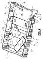
- FIGS. 1-5 illustrate an electronics enclosure E formed in accordance with the present development.
- the term "electronics enclosure” is intended to encompass a structure defining a space or recess adapted to receive and retain electronic components such as one or more printed circuit boards including electronic components mounted thereon.
- the enclosure E includes a body B comprising a plurality of side walls S1,S2,S3,S4 that define a periphery and also includes a top wall T that extends between and interconnects one end of the side walls S1 - S4.
- the side walls S1 - S4 and top wall T define a space or recess R adapted to receive and retain electronic components such as at least one printed circuit board PCB including electronic components mounted thereon as shown in FIG. 5 .
- the body B comprises a single mechanical package or component that is defined by a single metal body component M ( FIG. 4 ) and one or more polymeric body components P ( FIG. 4 ) that are overmolded onto the metal component M so as to be bonded or adhered to and mechanically interlocked with the metal body component M and, thus, inseparable from the metal body component M without physically damaging the metal and/or polymeric body components M, P.
- No fasteners such as screws, rivets or clips, are used to interconnect the polymeric component P to the metal component M.
- the body B includes only a single, one-piece polymeric body component P.
- FIG. 4 is an exploded isometric view that reveals the single metal body component M and the single polymeric body component P that is overmolded onto the metal body component M so as to define the single-component body B.
- the metal component M is defined from an electrically and thermally conductive metal such as aluminum, steel alloy or the like and is cast and/or otherwise defined as a one-piece construction.
- the polymeric component P is defined from an injection molded polymer ("plastic") that is overmolded to the metal component M after the metal component is placed in a mold. Accordingly, the polymeric material flows into voids defined in the metal component M and into voids defined between the metal component M and the associated mold component(s) in which the metal component M is positioned during the overmolding process.
- the polymeric component P includes various portions that are mechanically interlocked with the metal component M after the polymer used to mold the polymeric component P cools and hardens or cures, so that the metal component M and polymeric component P are not only adhered together but are also permanently mechanically interconnected through the overmolding process in which the molten polymeric material flows into voids of the metal component M such that the polymeric component P cannot be separated from the metal component M without destruction of the metal and/or polymeric component once the molding process is completed and the polymer cools and hardens or cures.
- the top wall T and at least one of the side walls S1 - S4 are defined by a combination of portions of the metal component M and one or more portions of the polymeric component P.
- the metal component M of the enclosure body B is superior for providing a first set of features and characteristics to the enclosure E.
- the strength of the metal component M makes it an ideal location for multiple mounting tabs MT including respective apertures that are adapted to be engaged by associated fasteners for securing the enclosure E to a desired mounting location or mating enclosure E.
- the mounting tabs MT are external to the recess R.
- the metal component M also provides a means for functional electrical/logic grounding.
- the metal component M includes one or more electrical contact regions EC that are located within the recess R and that are adapted to be electrically connected to one or more electronic components located in the recess R, such as the ground circuit of the printed circuit board PCB or an electrical component EB mounted thereon. As shown, the electrical contact regions EC are electrically connected to the printed circuit board PCB to provide electrical grounding for the electrical components mounted on the printed circuit board PCB.
- the metal component M can, itself, be connected to another electrical ground location such as a mounting rail, chassis or the like such that the metal component M provides an electrical grounding pathway between the electronic components PCB contained in the recess R and the associated electrical ground location to which the metal component M is electrically connected. It should be noted that the metal component M also shields the electronic contents of the recess R from electromagnetic interference (EMI).
- EMI electromagnetic interference
- the metal component M also provides a thermal pathway to conduct heat out of the enclosure recess R.
- the metal component includes or defines at least one heat sink HS.
- the heat sink HS is defined by a plurality of fins F separated from each other by airflow passages AP. The fins F follow a curved path to maximize the surface area in contact with the ambient air flowing through the passages AP.
- the polymeric component P of the enclosure body B is superior for providing a second set of features and characteristics to the enclosure E.
- the polymeric component P provides superior structural compliance and electrical insulation capabilities.
- portions P1 and P2 of the polymeric component P respectively cover internal surfaces of portions M1,M2 of the metal component M in the top wall T of the enclosure to electrically insulate the portions M1,M2 from electronic components contained in the enclosure recess R.
- the portions P1,P2 of the polymeric component P define electrical isolation zones that help to protect a user or other person from high-voltage or electrical charges that might otherwise be conducted through the metal component M.
- some or all of the electrical contact regions EC are defined by specially located openings or voids in the electrical isolation zone(s) P1,P2 that expose the underlying metal component M for desired electrical ground connections with the electronic components PCB.
- thermal transfer region TR ( FIG. 2 ) of the metal component M underlying each/the heat sink HS be exposed and not covered by isolation zones of the polymeric component P in order to maximize heat transfer from electronic components located in the recess R to the heat sink HS.
- the polymeric component P as overmolded to the metal component M, include a plurality of attachment features AF for securing one or more electronic components, such as a printed circuit board PCB, within the recess R.
- a first side wall portion PS1 of the polymeric component P defines part of the enclosure body side wall S1 and a second side wall portion PS2 of the polymeric component P defines part of the enclosure body side wall S2, and the attachment features AF are defined as part of the first and second side wall portions PS1,PS2.
- the attachment features AF of the in the illustrated embodiment are provided one or more printed circuit board retention nibs N defined by the first side wall portion PS1 and/or the second side wall portion PS2 of the polymeric component P.
- each nib N is dimensioned and conformed to capture the printed circuit board PCB in the recess R.
- a printed circuit board PCB is captured between each nib N of the polymeric portion P and another portion of the body defined by either the metal or polymeric component M,P.
- the nibs N capture the circuit board PCB against supports ST defined by either the metal component M or polymeric component P.
- each nib N located on at least one of the side wall portions PS1,PS2 be defined with a ramped surface N1 that diverges away from the side wall portion PS1,PS2 from which it projects as it extends deeper into the recess R toward the top wall T.
- the ramped surface N1 and the natural resiliency of the side wall portions PS1,PS2 of the polymeric portion P facilitates a sliding snap-fit engagement of a printed circuit board PCB into the recess R to a position where it is captured in the recess R by the nibs N as shown in FIG. 5 , without requiring use of additional fasteners. Also, the printed circuit board PCB can be removed from the recess R by resilient deflection of the polymeric side wall portions PS1,PS2 to disengage the printed circuit board PCB from each nib N.
- the attachment features AF can alternatively include or be defined by other structures of the polymeric component P that provide for a snap-fit engagement of a printed circuit board PCB or other electronic component with the body B to retain the printed circuit board PCB or other electronic component at a select desired location in the recess R, where at least one electronic component EB thereof is electrically connected to the metal component M through a contact region EC, at least one electronic component EB thereof is electrically isolated from the metal component M by an electrical isolation zone P1,P2 of the polymeric component P, and wherein at least another electronic component EB is located adjacent an uncovered thermal transfer region TR of the metal component M so as to be located to transfer heat into the thermal transfer region TR and to the associated heat sink HS adjacent/under which the thermal transfer region TR is located.
- the polymeric component P is also preferred relative to the metal component M for defining air flow slots U and other openings in the enclosure body B.
- the polymeric component P is injection molded to include such slots U and other openings for connectors and the like so that no milling of the metal component M or other post-processing of either the metal or polymeric component M,P is required once the polymeric component P is overmolded onto the metal component M.
Landscapes
- Engineering & Computer Science (AREA)
- Microelectronics & Electronic Packaging (AREA)
- Physics & Mathematics (AREA)
- Thermal Sciences (AREA)
- Cooling Or The Like Of Electrical Apparatus (AREA)
- Casings For Electric Apparatus (AREA)
- Structures For Mounting Electric Components On Printed Circuit Boards (AREA)
- Shielding Devices Or Components To Electric Or Magnetic Fields (AREA)
Applications Claiming Priority (1)
| Application Number | Priority Date | Filing Date | Title |
|---|---|---|---|
| US12/497,917 US8081466B2 (en) | 2009-07-06 | 2009-07-06 | Overmolded electronics enclosure |
Publications (2)
| Publication Number | Publication Date |
|---|---|
| EP2273861A2 true EP2273861A2 (de) | 2011-01-12 |
| EP2273861A3 EP2273861A3 (de) | 2012-08-22 |
Family
ID=43037183
Family Applications (1)
| Application Number | Title | Priority Date | Filing Date |
|---|---|---|---|
| EP10168566A Withdrawn EP2273861A3 (de) | 2009-07-06 | 2010-07-06 | Überformtes elektronisches Gehäuse |
Country Status (4)
| Country | Link |
|---|---|
| US (1) | US8081466B2 (de) |
| EP (1) | EP2273861A3 (de) |
| CN (1) | CN101945550B (de) |
| TW (1) | TWI523596B (de) |
Cited By (1)
| Publication number | Priority date | Publication date | Assignee | Title |
|---|---|---|---|---|
| CN109515348A (zh) * | 2017-09-19 | 2019-03-26 | 马涅蒂-马瑞利公司 | 用于车辆的电子单元 |
Families Citing this family (6)
| Publication number | Priority date | Publication date | Assignee | Title |
|---|---|---|---|---|
| USD688707S1 (en) * | 2012-05-16 | 2013-08-27 | Ge Intelligent Platforms, Inc. | Electronics enclosure |
| US10033242B2 (en) | 2013-02-01 | 2018-07-24 | Regal Beloit America, Inc. | Electrical machines and methods of assembling the same |
| USD707629S1 (en) | 2013-02-01 | 2014-06-24 | Regal Beloit America, Inc. | End cap |
| US10736247B2 (en) | 2018-12-06 | 2020-08-04 | Honeywell International Inc. | System and method with optimized polymer and metal structural components for electronic assembly |
| CA3162001A1 (en) * | 2019-11-26 | 2021-06-03 | Jpb Systeme | Instrumented, load-sensing washer |
| CN115669243A (zh) * | 2020-04-08 | 2023-01-31 | 申泰公司 | 管理电连接器和印刷电路板中不需要的热量、机械应力和emi |
Family Cites Families (33)
| Publication number | Priority date | Publication date | Assignee | Title |
|---|---|---|---|---|
| US4768286A (en) * | 1986-10-01 | 1988-09-06 | Eastman Christensen Co. | Printed circuit packaging for high vibration and temperature environments |
| US5015192A (en) * | 1989-11-13 | 1991-05-14 | Itt Corporation | Contact retention and sealing system |
| ES2057723T5 (es) * | 1991-12-11 | 1999-01-01 | Hewlett Packard Gmbh | Chasis de un dispositivo. |
| FR2703255A1 (fr) * | 1993-03-29 | 1994-10-07 | Ozen Sa | Corps creux, tel qu'une tête de club de golf, en matière thermoplastique moulée, comportant un insert emprisonné, et son procédé de fabrication. |
| US5387119A (en) * | 1993-10-08 | 1995-02-07 | Tescorp Seismic Products, Inc. | Waterproof electrical connector |
| US5675473A (en) * | 1996-02-23 | 1997-10-07 | Motorola, Inc. | Apparatus and method for shielding an electronic module from electromagnetic radiation |
| US5733145A (en) * | 1997-03-13 | 1998-03-31 | Tescorp Seismic Products, Inc. | Seal assembly for overmolded metal structure |
| US6180045B1 (en) * | 1998-05-20 | 2001-01-30 | Delco Electronics Corporation | Method of forming an overmolded electronic assembly |
| US6151219A (en) * | 1999-02-01 | 2000-11-21 | Itt Manufacturing Enterprises, Inc. | Electronic card with sheet metal and overmolded plastic frame parts |
| US6893523B2 (en) * | 1999-02-11 | 2005-05-17 | International Business Machines Corporation | Method for bonding heat sinks to overmold material |
| US6404596B1 (en) * | 2000-02-08 | 2002-06-11 | Seagate Technology Llc | Overmolding stiffening technique and structure |
| US6483719B1 (en) * | 2000-03-21 | 2002-11-19 | Spraylat Corporation | Conforming shielded form for electronic component assemblies |
| US6307749B1 (en) * | 2000-10-23 | 2001-10-23 | Delphi Technologies, Inc. | Overmolded electronic module with underfilled surface-mount components |
| DE10104998A1 (de) * | 2001-02-03 | 2002-08-22 | Hydac Electronic Gmbh | Schaltvorrichtung |
| US6807731B2 (en) * | 2002-04-02 | 2004-10-26 | Delphi Technologies, Inc. | Method for forming an electronic assembly |
| US6862181B1 (en) * | 2003-03-17 | 2005-03-01 | Unisys Corporation | Apparatus and method for shielding a circuit board |
| US6779260B1 (en) * | 2003-03-28 | 2004-08-24 | Delphi Technologies, Inc. | Overmolded electronic package including circuit-carrying substrate |
| US7132746B2 (en) * | 2003-08-18 | 2006-11-07 | Delphi Technologies, Inc. | Electronic assembly with solder-bonded heat sink |
| US7140969B2 (en) * | 2003-08-22 | 2006-11-28 | American Axle & Manufacturing, Inc. | Overmolded yoke assembly |
| US7372151B1 (en) * | 2003-09-12 | 2008-05-13 | Asat Ltd. | Ball grid array package and process for manufacturing same |
| JP4806395B2 (ja) * | 2004-02-27 | 2011-11-02 | グリーン, ツイード オブ デラウェア, インコーポレイテッド | 密閉電気コネクター |
| US7144259B2 (en) * | 2004-02-27 | 2006-12-05 | Finisar Corporation | Optical transceiver module having a dual segment molded lead frame connector |
| US7198987B1 (en) * | 2004-03-04 | 2007-04-03 | Skyworks Solutions, Inc. | Overmolded semiconductor package with an integrated EMI and RFI shield |
| US6966800B2 (en) * | 2004-03-22 | 2005-11-22 | Fci Americas Technology, Inc. | Overmolded electrical connector |
| US7230829B2 (en) * | 2005-01-28 | 2007-06-12 | Delphi Technologies, Inc. | Overmolded electronic assembly with insert molded heat sinks |
| US7319571B2 (en) * | 2005-02-23 | 2008-01-15 | Seagate Technology Llc | Overmold material and metal base interface design for leakage reduction in a disc drive |
| US7271513B2 (en) * | 2005-04-15 | 2007-09-18 | Seagate Technology Llc | Thermal stress relieved overmolded mounting base |
| US7514480B2 (en) * | 2005-06-21 | 2009-04-07 | Arkema Inc. | Low level radiation treatment for improving polymer properties |
| US7359144B2 (en) * | 2005-06-28 | 2008-04-15 | Seagate Technology Llc | Overmold component seal in an electronic device housing |
| US7372133B2 (en) * | 2005-12-01 | 2008-05-13 | Intel Corporation | Microelectronic package having a stiffening element and method of making same |
| JP2007250725A (ja) * | 2006-03-15 | 2007-09-27 | Nec Corp | 携帯端末装置 |
| US7486517B2 (en) * | 2006-12-20 | 2009-02-03 | Nokia Corporation | Hand-held portable electronic device having a heat spreader |
| US7616448B2 (en) * | 2007-09-14 | 2009-11-10 | Delphi Technologies, Inc. | Wrap-around overmold for electronic assembly |
-
2009
- 2009-07-06 US US12/497,917 patent/US8081466B2/en active Active
-
2010
- 2010-07-05 TW TW099121975A patent/TWI523596B/zh not_active IP Right Cessation
- 2010-07-06 CN CN201010224598.4A patent/CN101945550B/zh active Active
- 2010-07-06 EP EP10168566A patent/EP2273861A3/de not_active Withdrawn
Non-Patent Citations (1)
| Title |
|---|
| None |
Cited By (2)
| Publication number | Priority date | Publication date | Assignee | Title |
|---|---|---|---|---|
| CN109515348A (zh) * | 2017-09-19 | 2019-03-26 | 马涅蒂-马瑞利公司 | 用于车辆的电子单元 |
| CN109515348B (zh) * | 2017-09-19 | 2021-03-02 | 马涅蒂-马瑞利公司 | 用于车辆的电子单元 |
Also Published As
| Publication number | Publication date |
|---|---|
| TW201116189A (en) | 2011-05-01 |
| US8081466B2 (en) | 2011-12-20 |
| US20110002100A1 (en) | 2011-01-06 |
| CN101945550A (zh) | 2011-01-12 |
| TWI523596B (zh) | 2016-02-21 |
| EP2273861A3 (de) | 2012-08-22 |
| CN101945550B (zh) | 2014-05-07 |
Similar Documents
| Publication | Publication Date | Title |
|---|---|---|
| EP2273861A2 (de) | Überformtes elektronisches Gehäuse | |
| US8059416B2 (en) | Multi-cavity electromagnetic shielding device | |
| CN105409056B (zh) | 紧凑型屏蔽的车载雷达模块和方法 | |
| US20130058059A1 (en) | Electromagnetic wave shielding case | |
| US6341063B2 (en) | Installation structure of printed-circuit board for electronic control unit | |
| CN102044776B (zh) | 电连接器及其制造方法 | |
| CN101946381B (zh) | 电接线箱的防水结构 | |
| EP3589094A1 (de) | Elektronische einheit und verfahren zur herstellung davon | |
| CN206533249U (zh) | 电动助力转向装置用控制装置 | |
| US7701651B2 (en) | Lens module structure with a metal shell and assembling method therefor | |
| US6741476B2 (en) | Housing for use in a vehicle to accommodate a printed circuit board containing electronic components | |
| US11910544B2 (en) | Assembly of printed circuit board with overmolded epoxy to baseplate | |
| US20230352861A1 (en) | Thermal connection between printed circuit board and base plate with epoxy molded material | |
| US20090197478A1 (en) | Interlocking overmold for electronic assembly | |
| JP2013206951A (ja) | 電子装置 | |
| JP6166654B2 (ja) | 電子回路ユニットにおける外装ケースの成形方法 | |
| US20250258273A1 (en) | Radar Device And Method For Manufacturing The Same | |
| JP2017174992A (ja) | 電子制御ユニット | |
| US7654867B2 (en) | Receptacle connector assembly for IC card and IC card connector | |
| US12490388B2 (en) | Overmolded printed circuit board and connector with integrated stand-up mounting and ground connection | |
| KR101567091B1 (ko) | 콘덴서 결합 퓨즈 | |
| JP4666945B2 (ja) | パック電池 | |
| CN101166412B (zh) | 一种屏蔽盖的制造方法和利用该方法制造的屏蔽盖 | |
| US20120128407A1 (en) | Fastening Structure and Swarf Tray | |
| EP1515598B1 (de) | Abschirmvorrichtung für eine Leiterplatte und deren Herstellungsverfahren |
Legal Events
| Date | Code | Title | Description |
|---|---|---|---|
| PUAI | Public reference made under article 153(3) epc to a published international application that has entered the european phase |
Free format text: ORIGINAL CODE: 0009012 |
|
| AK | Designated contracting states |
Kind code of ref document: A2 Designated state(s): AL AT BE BG CH CY CZ DE DK EE ES FI FR GB GR HR HU IE IS IT LI LT LU LV MC MK MT NL NO PL PT RO SE SI SK SM TR |
|
| AX | Request for extension of the european patent |
Extension state: BA ME RS |
|
| PUAL | Search report despatched |
Free format text: ORIGINAL CODE: 0009013 |
|
| AK | Designated contracting states |
Kind code of ref document: A3 Designated state(s): AL AT BE BG CH CY CZ DE DK EE ES FI FR GB GR HR HU IE IS IT LI LT LU LV MC MK MT NL NO PL PT RO SE SI SK SM TR |
|
| AX | Request for extension of the european patent |
Extension state: BA ME RS |
|
| RIC1 | Information provided on ipc code assigned before grant |
Ipc: H05K 7/14 20060101AFI20120716BHEP Ipc: H05K 7/20 20060101ALI20120716BHEP |
|
| 17P | Request for examination filed |
Effective date: 20130222 |
|
| STAA | Information on the status of an ep patent application or granted ep patent |
Free format text: STATUS: THE APPLICATION IS DEEMED TO BE WITHDRAWN |
|
| 18D | Application deemed to be withdrawn |
Effective date: 20150106 |