EP2274760B1 - Circuit électrique comprenant un moyen de signalisation - Google Patents
Circuit électrique comprenant un moyen de signalisation Download PDFInfo
- Publication number
- EP2274760B1 EP2274760B1 EP09730964.5A EP09730964A EP2274760B1 EP 2274760 B1 EP2274760 B1 EP 2274760B1 EP 09730964 A EP09730964 A EP 09730964A EP 2274760 B1 EP2274760 B1 EP 2274760B1
- Authority
- EP
- European Patent Office
- Prior art keywords
- signaling
- electrical circuit
- circuit according
- electrical
- functional state
- Prior art date
- Legal status (The legal status is an assumption and is not a legal conclusion. Google has not performed a legal analysis and makes no representation as to the accuracy of the status listed.)
- Active
Links
Images


Classifications
-
- H—ELECTRICITY
- H01—ELECTRIC ELEMENTS
- H01H—ELECTRIC SWITCHES; RELAYS; SELECTORS; EMERGENCY PROTECTIVE DEVICES
- H01H71/00—Details of the protective switches or relays covered by groups H01H73/00 - H01H83/00
- H01H71/04—Means for indicating condition of the switching device
-
- H—ELECTRICITY
- H01—ELECTRIC ELEMENTS
- H01H—ELECTRIC SWITCHES; RELAYS; SELECTORS; EMERGENCY PROTECTIVE DEVICES
- H01H71/00—Details of the protective switches or relays covered by groups H01H73/00 - H01H83/00
- H01H71/04—Means for indicating condition of the switching device
- H01H2071/042—Means for indicating condition of the switching device with different indications for different conditions, e.g. contact position, overload, short circuit or earth leakage
Definitions
- the invention relates to an electrical circuit according to the preamble of claim 1.
- Electrical systems such as electrical systems or electrical lines are, to ensure trouble-free operation, protected from interference events by protective devices against impairment of their function and / or against destruction.
- the electrical circuits in question with a means for signaling signal at least one functional state, such as functional or defective, a protective device.
- a functional state such as functional or defective
- the functional state of a protective device to be monitored is directly perceptible via a signaling, for example via optical signaling.
- a malfunction event is understood to mean an event by which electrical energy is applied to an electrical system in such a way that the electrical system is impaired or destroyed in its proper function.
- interference events are lightning or static discharges as a result of overvoltage pulses and / or overcurrent pulses, for example, galvanic, inductive or capacitive, are coupled into the electrical system and impair or destroy its function.
- Protection against over-voltage pulses have protective elements, u. For example, spark gaps, varistors, diodes, suppressor diodes, and are known in the art. Such protective devices are also referred to as OVP (over voltage protection).
- an interference event in the context of the present invention is understood to mean an overcurrent with which an electrical system, for example an electrical line, can be overloaded and / or destroyed, for example, by a short circuit or ground fault.
- Protective devices for protection against overcurrents are colloquially referred to as fuses and are the skilled person in various Versions, for example in the form of fuses or circuit breakers, known.
- FIGS Fig. 3a and 3b Shown is a fuse connecting two electrical switching points. To signal a functional state of the fuse, this is connected in parallel to a series circuit of a series resistor and an opposite parallel connection of two LEDs. If the fuse is functional, the voltage prevailing between the two circuit points is too small to supply the LEDs with sufficient voltage to light up. If the fuse, for example, destroyed by a high current and therefore interrupts the flow of current, so the voltage between the two points and the LEDs are supplied with sufficient voltage to a functional state, here a defect in the fuse signaling. It is clear that depending on the type of voltage, DC or AC voltage only one or both LEDs light up.
- a circuit according to the preamble of claim 1 is known from EP-A-1 628 317 known.
- a disadvantage of the known circuits is that the means used for signaling, such as a light emitting diode, to maintain the signaling electrical energy and cause a retroactive effect on the function monitoring protective device and / or an electrical energy-providing device.
- a signaling device which is pulse-activatable and bistable, has no circuit feedback after pulse activation and is designed for permanent, powerless signaling.
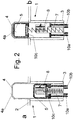
- Fig. 1a shows a signaling device 1 with a, for example, held in a housing 2 housing 3.
- the housing 3 is elongated and has at its upper end 4 a possibly transparent designed end 4a.
- a signaling element 5 is slidably disposed within the housing 3.
- the signaling element 5 is between a first position (which signals a first functional state) (as in FIG Fig. 1 a and 2a shown) and a - a second functional state signaling - second position (as in Fig. 1b and 2a represented) by a force element, for example by a spring 7 slidably.
- the signaling means 1 further comprises a locking means 8 with a locking lug 8a, which first the signaling element 5 in the first position ( Fig. 1a and 2a ) arrested.
- the detent lug 8a engages in a corresponding inner opening 8b of the signaling element 5.
- a, for example, designed as an electromagnet 9 pull element is pulse-activated so the detent 8a is brought in a pulse activation of the electromagnet 9 out of engagement with the arranged on the inside of the signaling element 5 opening 8b. Due to the force of the spring 7, the signaling element 5 is moved from the first to the second position.
- the pulse activation of the electromagnet 9 is effected by application of an electrical pulse, via electrical connection means, for example via the conductors 9a, 9b and the contact pins 9c, 9d.
- signaling means 1 is configured only for optical signaling of a functional state.
- the signaling element 5 is designed monochrome or multicolor and visible through the optically transparent executed end 4a of the housing 3 when it is in the second position ( Fig. 1b ).
- the in Fig. 2a and 2b illustrated signaling element 5 means for electrical signaling, for example, the contact pins 10a and 10b and the contact connector 10c.
- an opener is realized, wherein the opener opens when the signaling element 5 from the first position ( Fig. 2a ) into a second position ( Fig. 2b ) is moved.
- the Fig. 2a and 2b Not shown means for pulse activation provided with reference numerals.
- Fig. 3a and 3b show a known from the prior art monitoring a fuse 11 by means of anti-parallel light emitting diodes 12. The operation of this circuit has already been explained in the introduction to the description.
- the light-emitting diode arrangement 12 known from the prior art is replaced by the signaling means 5 according to the invention.
- the via the contact pins 9c, 9d (see Fig. 1a and 1b ) pulse activatable electromagnet 9 (see Fig. 1a and 1b ) in series with the opener formed by the means 10a, 10b and 10c (see Fig. 2a and 2b ).
- the opening contact of the signaling means 5 opens as described above.
- the current flow through the electromagnet is thereby interrupted, the electromagnet 9 is de-energized and thus does not absorb electrical power.
- the signaling element 5 remains in the second position, as in FIG Fig. 4b shown (compare also Fig. 1b and 2 B ) and permanently signals the functional state of the protection device.
- opening the opener see. FIGS. 2a and 2b , 10a, 10b and 10c
- the galvanic connection between the circuit points 13 and 14 is interrupted, so that by the signaling element 5 has no effect on the circuit and the protection device to be monitored, here the fuse 11.
- the signaling means 5 further comprises an unillustrated electrically operated restoring device with which the signaling element 5 can be reset from the second back to the first position, for example after a successful repair of a protective device to be monitored.
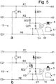
- a protection device 15 for protecting electrical systems against overvoltages and the signaling device 5 according to the invention is shown.
- spark gaps between two branches E1-A1 and E3-A3 and between two branches E2-A2 and E3-A3 lies in the entrance area of the protective device 15, both spark gaps being accommodated in a component designated FS in the present embodiment.
- This part of the protection device is considered coarse protection denotes and "destroys" most of the injected by a disturbance event in the protection device 15 energy.
- the remaining part of the protection device 15 is referred to as fine protection and serves primarily to limit the voltages occurring to a safe level for the electrical system to be protected.
- An input terminal E1 is connected via a resistor R1 to an output terminal A1. Parallel to the output terminal A1 and to a lying on PE potential output terminal A3 is a series circuit of a suppressor diode SD1 and anti-parallel diodes D1 and D2. Accordingly, an input terminal E2 is connected via a resistor R2 to an output terminal A2, parallel to the output terminal A2 and lying at PE potential output terminal A3 is a series circuit of a suppressor diode SD2 and the antiparallel connected diodes D1 and D2.
- An unillustrated electrical system to be protected against disturbance events for example a measuring amplifier or an industrial PC, is connected to the protective device 15 via the output terminals A1 to A3.
- the input terminals E1-E3 are in turn connected to signal sources and / or to devices supplying electrical energy, for example an electrical supply network.
- the installation and the interconnection of the protective device 15 and the electrical system to be protected takes place in such a way that, in the event of an interference event, coupled-in electrical energy is coupled in on the input side of the protective device 15. This is known to the person skilled in the art.
- the circuit shown in the Fig. 5a and 5b also has a state recognition device 16 which monitors the protection device 15 and, in the event of a defect in the protection device 15, acts on the connected signaling device 5 with an electrical signal, for example in the form of an electrical pulse. By such a pulse, the signaling means 5 is activated, so that, as already stated, a permanent and powerless signaling of the functional state of the protective device 15 takes place. Furthermore, here also a non-reaction by the on hand Fig. 4a and 4b explained interconnections can be achieved with the realized by the means 10a, 10b and 10c opener (see. FIGS. 2a and 2b , 10a, 10b and 10c).
- the signaling means 5 may additionally to the contact already described a further contact 17, for example, for retransmission of a functional state and a non-illustrated higher-level electrical system having.
Landscapes
- Emergency Protection Circuit Devices (AREA)
- Fuses (AREA)
- Keying Circuit Devices (AREA)
- Electronic Switches (AREA)
Claims (7)
- Circuit électrique présentant un dispositif de protection (11, 15) pour protéger des systèmes électriques des événements perturbateurs et des moyens (1) pour signaler au moins un état de fonctionnement du dispositif de protection (11, 15), le moyen de signalisation (1) étant activable par une impulsion et bistable, ne présentant pas de rétroaction sur le circuit après une activation par une impulsion et étant équipé en vue d'une signalisation durable sans fil, caractérisé en ce que le dispositif de protection présente un dispositif de protection contre les surtensions (15) et en ce que le moyen de signalisation (1) présente un boîtier (3) de forme allongée avec une extrémité supérieure (4) munie d'une fermeture (4a) transparente et un élément de signalisation (5), l'élément de signalisation (5) étant disposé avec possibilité de translation à l'intérieur du boîtier (3) et le boîtier (3) étant retenu dans une paroi du boîtier (2) et le moyen de signalisation (1) présentant un dispositif de réinitialisation à actionnement électrique avec lequel l'élément de signalisation (5) peut être ramené de la deuxième position à la première.
- Circuit électrique selon la revendication 1, caractérisé en ce que le moyen de signalisation (1) signale l'au moins un état de fonctionnement de façon visuelle et/ou électrique.
- Circuit électrique selon l'une des revendications précédentes, caractérisé en ce que l'élément de signalisation (5) peut être déplacé d'une première position signalant un premier état de fonctionnement (Fig. 1 a, 2a) à une deuxième position signalant un deuxième état de fonctionnement (Fig. 1 b, 2b), l'élément de signalisation (5) étant bloqué dans la première position par un moyen de blocage (8) pouvant être débloqué par une activation par une impulsion et l'élément de signalisation (5) pouvant être déplacé, après une activation par une impulsion du moyen de blocage (8), de la première position à la deuxième position au moyen d'un élément de force (7).
- Circuit électrique selon l'une des revendications précédentes, caractérisé en ce que l'élément de force (7) est réalisé comme un ressort.
- Circuit électrique selon l'une des revendications précédentes, caractérisé en ce que l'élément de signalisation (5) est réalisé d'une seule couleur aux fins de signalisation visuelle.
- Circuit électrique selon l'une des revendications précédentes, caractérisé en ce que l'élément de signalisation (5) est réalisé de plusieurs couleurs aux fins de signalisation visuelle.
- Circuit électrique selon l'une des revendications précédentes, caractérisé en ce que le dispositif de protection comprend un disjoncteur de protection de ligne (11).
Priority Applications (1)
| Application Number | Priority Date | Filing Date | Title |
|---|---|---|---|
| SI200931666A SI2274760T1 (sl) | 2008-04-11 | 2009-03-12 | Električno vezje s sredstvom za signaliziranje |
Applications Claiming Priority (2)
| Application Number | Priority Date | Filing Date | Title |
|---|---|---|---|
| DE202008005085U DE202008005085U1 (de) | 2008-04-11 | 2008-04-11 | Elektrische Schaltung mit einem Mittel zur Signalisierung |
| PCT/EP2009/052907 WO2009124820A1 (fr) | 2008-04-11 | 2009-03-12 | Circuit électrique comprenant un moyen de signalisation |
Publications (2)
| Publication Number | Publication Date |
|---|---|
| EP2274760A1 EP2274760A1 (fr) | 2011-01-19 |
| EP2274760B1 true EP2274760B1 (fr) | 2017-04-19 |
Family
ID=40672550
Family Applications (1)
| Application Number | Title | Priority Date | Filing Date |
|---|---|---|---|
| EP09730964.5A Active EP2274760B1 (fr) | 2008-04-11 | 2009-03-12 | Circuit électrique comprenant un moyen de signalisation |
Country Status (6)
| Country | Link |
|---|---|
| US (1) | US8379362B2 (fr) |
| EP (1) | EP2274760B1 (fr) |
| DE (1) | DE202008005085U1 (fr) |
| ES (1) | ES2631479T3 (fr) |
| SI (1) | SI2274760T1 (fr) |
| WO (1) | WO2009124820A1 (fr) |
Families Citing this family (5)
| Publication number | Priority date | Publication date | Assignee | Title |
|---|---|---|---|---|
| DE102011112474B4 (de) * | 2011-09-05 | 2017-07-13 | Dehn + Söhne Gmbh + Co. Kg | Verfahren und Anordnung zum Überspannungsschutz von Wechselrichtern für photovoltaische Anlagen |
| DE102016203506B4 (de) * | 2016-03-03 | 2021-10-07 | Siemens Aktiengesellschaft | Auslösevorrichtung und elektromechanisches Schutzschaltgerät |
| DE102016011815B3 (de) * | 2016-10-05 | 2018-02-15 | IAD Gesellschaft für Informatik, Automatisierung und Datenverarbeitung mbH | Betriebsgerät mit gestaffeltem Überspannungs- und Überstromschutz für die Ansteuerung von intelligenten Leuchtmitteln und Geräten sowie Leuchtmittel mit diesem Betriebsgerät |
| DE102017129657A1 (de) * | 2017-07-10 | 2019-01-10 | Dehn + Söhne Gmbh + Co. Kg | Anordnung zur nicht-reversiblen Detektion und Anzeige von elektrischen Überströmen oder Stromgrenzwerten mittels eines vorkonfektionierten Leiters |
| CN113514715A (zh) * | 2021-04-20 | 2021-10-19 | 核工业西南物理研究院 | 一种大量电容并联时单个电容过流故障实时指示电路 |
Citations (2)
| Publication number | Priority date | Publication date | Assignee | Title |
|---|---|---|---|---|
| US3308404A (en) * | 1964-02-10 | 1967-03-07 | Fujita Teizo | Electric switch responsive to predetermined or abnormal current condition |
| EP1826795A1 (fr) * | 2006-02-24 | 2007-08-29 | ABB France | Dispositif de protection contre les surtension avec système de visualisation simplifié et procédé de fabrication correspondant |
Family Cites Families (6)
| Publication number | Priority date | Publication date | Assignee | Title |
|---|---|---|---|---|
| US4382270A (en) * | 1981-04-07 | 1983-05-03 | Westinghouse Electric Corp. | Ground fault circuit breaker with mechanical indicator for ground fault trips |
| ZA864209B (en) * | 1985-07-03 | 1987-02-25 | Westinghouse Electric Corp | Ground fault receptacle with compact component arrangement |
| DE3634456C1 (en) * | 1986-10-09 | 1988-02-11 | Kopp Gmbh & Co Kg Heinrich | Remotely controllable line protection circuit breaker having a switching status indication |
| DE19735415A1 (de) | 1997-08-14 | 1999-02-18 | Siemens Ag | Schaltmechanismus für einen Schutzschalter |
| US7173799B1 (en) * | 2004-02-03 | 2007-02-06 | Pass & Seymour, Inc. | Protection device with a sandwiched cantilever breaker mechanism |
| DE102004040288B4 (de) | 2004-08-19 | 2007-09-20 | Siemens Ag | Schutzschalter mit Kurzschluss- und Überlastauslöseanzeige sowie entsprechendes Verfahren |
-
2008
- 2008-04-11 DE DE202008005085U patent/DE202008005085U1/de not_active Expired - Lifetime
-
2009
- 2009-03-12 EP EP09730964.5A patent/EP2274760B1/fr active Active
- 2009-03-12 US US12/936,994 patent/US8379362B2/en not_active Expired - Fee Related
- 2009-03-12 SI SI200931666A patent/SI2274760T1/sl unknown
- 2009-03-12 ES ES09730964.5T patent/ES2631479T3/es active Active
- 2009-03-12 WO PCT/EP2009/052907 patent/WO2009124820A1/fr not_active Ceased
Patent Citations (2)
| Publication number | Priority date | Publication date | Assignee | Title |
|---|---|---|---|---|
| US3308404A (en) * | 1964-02-10 | 1967-03-07 | Fujita Teizo | Electric switch responsive to predetermined or abnormal current condition |
| EP1826795A1 (fr) * | 2006-02-24 | 2007-08-29 | ABB France | Dispositif de protection contre les surtension avec système de visualisation simplifié et procédé de fabrication correspondant |
Also Published As
| Publication number | Publication date |
|---|---|
| US20110038089A1 (en) | 2011-02-17 |
| US8379362B2 (en) | 2013-02-19 |
| SI2274760T1 (sl) | 2017-07-31 |
| WO2009124820A1 (fr) | 2009-10-15 |
| ES2631479T3 (es) | 2017-08-31 |
| DE202008005085U1 (de) | 2009-08-20 |
| EP2274760A1 (fr) | 2011-01-19 |
Similar Documents
| Publication | Publication Date | Title |
|---|---|---|
| EP2145368B1 (fr) | Circuit comprenant au moins deux condensateurs branchés en série | |
| DE3231143C2 (de) | Verpol- und Überspannungsschutzschaltung für elektronische Verbraucher | |
| DE3832068C2 (fr) | ||
| DE60115248T2 (de) | Überspannungsschutzsystem | |
| EP2182605B1 (fr) | Agencement de commutation pour la protection de dispositifs électroniques contre des tensions logiques erronées | |
| EP2104974B1 (fr) | Dispositif de protection contre les surtensions pour un appareil électronique | |
| EP2274760B1 (fr) | Circuit électrique comprenant un moyen de signalisation | |
| DE102007043512A1 (de) | Energiewandleranlage | |
| EP3501074B1 (fr) | Protection contre les surtensions | |
| EP2272146B1 (fr) | Dispositif de protection | |
| DE4124321A1 (de) | Anordnung zur ableitung von ueberspannungen | |
| EP3128624B1 (fr) | Systeme de parasurtenseurs | |
| WO2009121770A1 (fr) | Dispositif de protection | |
| DE3852088T2 (de) | Elektrische Sicherheitsbarrieren. | |
| WO2002071600A2 (fr) | Dispositif de commutation de securite | |
| DE102011115722B4 (de) | Überspannungsschutzgerät | |
| DE4015301C2 (de) | Überspannungsschutzeinrichtung für elektrische Anlagen | |
| EP2608343B1 (fr) | Alimentation électrique | |
| AT409193B (de) | Schaltungsanordnung | |
| DE60028941T2 (de) | Überspannungsableiter für elektrische starkstromanlagen | |
| DE102020206250B3 (de) | Überspannungsschutz | |
| DE102012222782A1 (de) | Schaltvorrichtung mit Überspannungsschutz | |
| EP1353430B1 (fr) | Disposition de circuit | |
| EP2266176B1 (fr) | Dispositif de surveillance | |
| EP2127053A1 (fr) | Appareil de protection |
Legal Events
| Date | Code | Title | Description |
|---|---|---|---|
| PUAI | Public reference made under article 153(3) epc to a published international application that has entered the european phase |
Free format text: ORIGINAL CODE: 0009012 |
|
| 17P | Request for examination filed |
Effective date: 20101110 |
|
| AK | Designated contracting states |
Kind code of ref document: A1 Designated state(s): AT BE BG CH CY CZ DE DK EE ES FI FR GB GR HR HU IE IS IT LI LT LU LV MC MK MT NL NO PL PT RO SE SI SK TR |
|
| AX | Request for extension of the european patent |
Extension state: AL BA RS |
|
| DAX | Request for extension of the european patent (deleted) | ||
| 17Q | First examination report despatched |
Effective date: 20160126 |
|
| GRAP | Despatch of communication of intention to grant a patent |
Free format text: ORIGINAL CODE: EPIDOSNIGR1 |
|
| INTG | Intention to grant announced |
Effective date: 20161208 |
|
| GRAS | Grant fee paid |
Free format text: ORIGINAL CODE: EPIDOSNIGR3 |
|
| GRAA | (expected) grant |
Free format text: ORIGINAL CODE: 0009210 |
|
| AK | Designated contracting states |
Kind code of ref document: B1 Designated state(s): AT BE BG CH CY CZ DE DK EE ES FI FR GB GR HR HU IE IS IT LI LT LU LV MC MK MT NL NO PL PT RO SE SI SK TR |
|
| REG | Reference to a national code |
Ref country code: GB Ref legal event code: FG4D Free format text: NOT ENGLISH |
|
| REG | Reference to a national code |
Ref country code: CH Ref legal event code: EP |
|
| REG | Reference to a national code |
Ref country code: AT Ref legal event code: REF Ref document number: 886675 Country of ref document: AT Kind code of ref document: T Effective date: 20170515 |
|
| REG | Reference to a national code |
Ref country code: IE Ref legal event code: FG4D Free format text: LANGUAGE OF EP DOCUMENT: GERMAN |
|
| REG | Reference to a national code |
Ref country code: DE Ref legal event code: R096 Ref document number: 502009013884 Country of ref document: DE |
|
| REG | Reference to a national code |
Ref country code: NL Ref legal event code: MP Effective date: 20170419 |
|
| REG | Reference to a national code |
Ref country code: ES Ref legal event code: FG2A Ref document number: 2631479 Country of ref document: ES Kind code of ref document: T3 Effective date: 20170831 |
|
| REG | Reference to a national code |
Ref country code: LT Ref legal event code: MG4D |
|
| PG25 | Lapsed in a contracting state [announced via postgrant information from national office to epo] |
Ref country code: NL Free format text: LAPSE BECAUSE OF FAILURE TO SUBMIT A TRANSLATION OF THE DESCRIPTION OR TO PAY THE FEE WITHIN THE PRESCRIBED TIME-LIMIT Effective date: 20170419 |
|
| PG25 | Lapsed in a contracting state [announced via postgrant information from national office to epo] |
Ref country code: NO Free format text: LAPSE BECAUSE OF FAILURE TO SUBMIT A TRANSLATION OF THE DESCRIPTION OR TO PAY THE FEE WITHIN THE PRESCRIBED TIME-LIMIT Effective date: 20170719 Ref country code: FI Free format text: LAPSE BECAUSE OF FAILURE TO SUBMIT A TRANSLATION OF THE DESCRIPTION OR TO PAY THE FEE WITHIN THE PRESCRIBED TIME-LIMIT Effective date: 20170419 Ref country code: LT Free format text: LAPSE BECAUSE OF FAILURE TO SUBMIT A TRANSLATION OF THE DESCRIPTION OR TO PAY THE FEE WITHIN THE PRESCRIBED TIME-LIMIT Effective date: 20170419 Ref country code: GR Free format text: LAPSE BECAUSE OF FAILURE TO SUBMIT A TRANSLATION OF THE DESCRIPTION OR TO PAY THE FEE WITHIN THE PRESCRIBED TIME-LIMIT Effective date: 20170720 Ref country code: HR Free format text: LAPSE BECAUSE OF FAILURE TO SUBMIT A TRANSLATION OF THE DESCRIPTION OR TO PAY THE FEE WITHIN THE PRESCRIBED TIME-LIMIT Effective date: 20170419 |
|
| PG25 | Lapsed in a contracting state [announced via postgrant information from national office to epo] |
Ref country code: LV Free format text: LAPSE BECAUSE OF FAILURE TO SUBMIT A TRANSLATION OF THE DESCRIPTION OR TO PAY THE FEE WITHIN THE PRESCRIBED TIME-LIMIT Effective date: 20170419 Ref country code: PL Free format text: LAPSE BECAUSE OF FAILURE TO SUBMIT A TRANSLATION OF THE DESCRIPTION OR TO PAY THE FEE WITHIN THE PRESCRIBED TIME-LIMIT Effective date: 20170419 Ref country code: SE Free format text: LAPSE BECAUSE OF FAILURE TO SUBMIT A TRANSLATION OF THE DESCRIPTION OR TO PAY THE FEE WITHIN THE PRESCRIBED TIME-LIMIT Effective date: 20170419 Ref country code: BG Free format text: LAPSE BECAUSE OF FAILURE TO SUBMIT A TRANSLATION OF THE DESCRIPTION OR TO PAY THE FEE WITHIN THE PRESCRIBED TIME-LIMIT Effective date: 20170719 Ref country code: IS Free format text: LAPSE BECAUSE OF FAILURE TO SUBMIT A TRANSLATION OF THE DESCRIPTION OR TO PAY THE FEE WITHIN THE PRESCRIBED TIME-LIMIT Effective date: 20170819 |
|
| REG | Reference to a national code |
Ref country code: DE Ref legal event code: R097 Ref document number: 502009013884 Country of ref document: DE |
|
| PG25 | Lapsed in a contracting state [announced via postgrant information from national office to epo] |
Ref country code: SK Free format text: LAPSE BECAUSE OF FAILURE TO SUBMIT A TRANSLATION OF THE DESCRIPTION OR TO PAY THE FEE WITHIN THE PRESCRIBED TIME-LIMIT Effective date: 20170419 Ref country code: RO Free format text: LAPSE BECAUSE OF FAILURE TO SUBMIT A TRANSLATION OF THE DESCRIPTION OR TO PAY THE FEE WITHIN THE PRESCRIBED TIME-LIMIT Effective date: 20170419 Ref country code: EE Free format text: LAPSE BECAUSE OF FAILURE TO SUBMIT A TRANSLATION OF THE DESCRIPTION OR TO PAY THE FEE WITHIN THE PRESCRIBED TIME-LIMIT Effective date: 20170419 Ref country code: DK Free format text: LAPSE BECAUSE OF FAILURE TO SUBMIT A TRANSLATION OF THE DESCRIPTION OR TO PAY THE FEE WITHIN THE PRESCRIBED TIME-LIMIT Effective date: 20170419 |
|
| PLBE | No opposition filed within time limit |
Free format text: ORIGINAL CODE: 0009261 |
|
| STAA | Information on the status of an ep patent application or granted ep patent |
Free format text: STATUS: NO OPPOSITION FILED WITHIN TIME LIMIT |
|
| 26N | No opposition filed |
Effective date: 20180122 |
|
| REG | Reference to a national code |
Ref country code: FR Ref legal event code: PLFP Year of fee payment: 10 |
|
| PG25 | Lapsed in a contracting state [announced via postgrant information from national office to epo] |
Ref country code: MT Free format text: LAPSE BECAUSE OF FAILURE TO SUBMIT A TRANSLATION OF THE DESCRIPTION OR TO PAY THE FEE WITHIN THE PRESCRIBED TIME-LIMIT Effective date: 20170419 |
|
| REG | Reference to a national code |
Ref country code: CH Ref legal event code: PL |
|
| PG25 | Lapsed in a contracting state [announced via postgrant information from national office to epo] |
Ref country code: MC Free format text: LAPSE BECAUSE OF FAILURE TO SUBMIT A TRANSLATION OF THE DESCRIPTION OR TO PAY THE FEE WITHIN THE PRESCRIBED TIME-LIMIT Effective date: 20170419 |
|
| REG | Reference to a national code |
Ref country code: BE Ref legal event code: MM Effective date: 20180331 |
|
| REG | Reference to a national code |
Ref country code: IE Ref legal event code: MM4A |
|
| PG25 | Lapsed in a contracting state [announced via postgrant information from national office to epo] |
Ref country code: LU Free format text: LAPSE BECAUSE OF NON-PAYMENT OF DUE FEES Effective date: 20180312 |
|
| PG25 | Lapsed in a contracting state [announced via postgrant information from national office to epo] |
Ref country code: IE Free format text: LAPSE BECAUSE OF NON-PAYMENT OF DUE FEES Effective date: 20180312 |
|
| PG25 | Lapsed in a contracting state [announced via postgrant information from national office to epo] |
Ref country code: BE Free format text: LAPSE BECAUSE OF NON-PAYMENT OF DUE FEES Effective date: 20180331 Ref country code: CH Free format text: LAPSE BECAUSE OF NON-PAYMENT OF DUE FEES Effective date: 20180331 Ref country code: LI Free format text: LAPSE BECAUSE OF NON-PAYMENT OF DUE FEES Effective date: 20180331 |
|
| REG | Reference to a national code |
Ref country code: AT Ref legal event code: MM01 Ref document number: 886675 Country of ref document: AT Kind code of ref document: T Effective date: 20180312 |
|
| PG25 | Lapsed in a contracting state [announced via postgrant information from national office to epo] |
Ref country code: AT Free format text: LAPSE BECAUSE OF NON-PAYMENT OF DUE FEES Effective date: 20180312 |
|
| PG25 | Lapsed in a contracting state [announced via postgrant information from national office to epo] |
Ref country code: TR Free format text: LAPSE BECAUSE OF FAILURE TO SUBMIT A TRANSLATION OF THE DESCRIPTION OR TO PAY THE FEE WITHIN THE PRESCRIBED TIME-LIMIT Effective date: 20170419 |
|
| PG25 | Lapsed in a contracting state [announced via postgrant information from national office to epo] |
Ref country code: PT Free format text: LAPSE BECAUSE OF FAILURE TO SUBMIT A TRANSLATION OF THE DESCRIPTION OR TO PAY THE FEE WITHIN THE PRESCRIBED TIME-LIMIT Effective date: 20170419 Ref country code: HU Free format text: LAPSE BECAUSE OF FAILURE TO SUBMIT A TRANSLATION OF THE DESCRIPTION OR TO PAY THE FEE WITHIN THE PRESCRIBED TIME-LIMIT; INVALID AB INITIO Effective date: 20090312 |
|
| PG25 | Lapsed in a contracting state [announced via postgrant information from national office to epo] |
Ref country code: CY Free format text: LAPSE BECAUSE OF FAILURE TO SUBMIT A TRANSLATION OF THE DESCRIPTION OR TO PAY THE FEE WITHIN THE PRESCRIBED TIME-LIMIT Effective date: 20170419 Ref country code: MK Free format text: LAPSE BECAUSE OF NON-PAYMENT OF DUE FEES Effective date: 20170419 |
|
| PGFP | Annual fee paid to national office [announced via postgrant information from national office to epo] |
Ref country code: FR Payment date: 20230322 Year of fee payment: 15 Ref country code: CZ Payment date: 20230306 Year of fee payment: 15 |
|
| PGFP | Annual fee paid to national office [announced via postgrant information from national office to epo] |
Ref country code: GB Payment date: 20230321 Year of fee payment: 15 |
|
| P01 | Opt-out of the competence of the unified patent court (upc) registered |
Effective date: 20230523 |
|
| PGFP | Annual fee paid to national office [announced via postgrant information from national office to epo] |
Ref country code: IT Payment date: 20230328 Year of fee payment: 15 Ref country code: ES Payment date: 20230529 Year of fee payment: 15 |
|
| PG25 | Lapsed in a contracting state [announced via postgrant information from national office to epo] |
Ref country code: CZ Free format text: LAPSE BECAUSE OF NON-PAYMENT OF DUE FEES Effective date: 20240312 |
|
| PG25 | Lapsed in a contracting state [announced via postgrant information from national office to epo] |
Ref country code: CZ Free format text: LAPSE BECAUSE OF NON-PAYMENT OF DUE FEES Effective date: 20240312 |
|
| GBPC | Gb: european patent ceased through non-payment of renewal fee |
Effective date: 20240312 |
|
| PG25 | Lapsed in a contracting state [announced via postgrant information from national office to epo] |
Ref country code: GB Free format text: LAPSE BECAUSE OF NON-PAYMENT OF DUE FEES Effective date: 20240312 |
|
| PG25 | Lapsed in a contracting state [announced via postgrant information from national office to epo] |
Ref country code: FR Free format text: LAPSE BECAUSE OF NON-PAYMENT OF DUE FEES Effective date: 20240331 |
|
| PG25 | Lapsed in a contracting state [announced via postgrant information from national office to epo] |
Ref country code: GB Free format text: LAPSE BECAUSE OF NON-PAYMENT OF DUE FEES Effective date: 20240312 Ref country code: FR Free format text: LAPSE BECAUSE OF NON-PAYMENT OF DUE FEES Effective date: 20240331 |
|
| PGFP | Annual fee paid to national office [announced via postgrant information from national office to epo] |
Ref country code: DE Payment date: 20250319 Year of fee payment: 17 |
|
| PGFP | Annual fee paid to national office [announced via postgrant information from national office to epo] |
Ref country code: SI Payment date: 20250227 Year of fee payment: 17 |
|
| PG25 | Lapsed in a contracting state [announced via postgrant information from national office to epo] |
Ref country code: IT Free format text: LAPSE BECAUSE OF NON-PAYMENT OF DUE FEES Effective date: 20240312 |
|
| REG | Reference to a national code |
Ref country code: ES Ref legal event code: FD2A Effective date: 20250429 |
|
| PG25 | Lapsed in a contracting state [announced via postgrant information from national office to epo] |
Ref country code: ES Free format text: LAPSE BECAUSE OF NON-PAYMENT OF DUE FEES Effective date: 20240313 |