EP2276018A1 - Farbkorrektur in einem Bildanzeigegerät - Google Patents
Farbkorrektur in einem Bildanzeigegerät Download PDFInfo
- Publication number
- EP2276018A1 EP2276018A1 EP10010474A EP10010474A EP2276018A1 EP 2276018 A1 EP2276018 A1 EP 2276018A1 EP 10010474 A EP10010474 A EP 10010474A EP 10010474 A EP10010474 A EP 10010474A EP 2276018 A1 EP2276018 A1 EP 2276018A1
- Authority
- EP
- European Patent Office
- Prior art keywords
- pixels
- image
- data
- colour
- image display
- Prior art date
- Legal status (The legal status is an assumption and is not a legal conclusion. Google has not performed a legal analysis and makes no representation as to the accuracy of the status listed.)
- Withdrawn
Links
Images





Classifications
-
- H—ELECTRICITY
- H04—ELECTRIC COMMUNICATION TECHNIQUE
- H04N—PICTORIAL COMMUNICATION, e.g. TELEVISION
- H04N9/00—Details of colour television systems
- H04N9/77—Circuits for processing the brightness signal and the chrominance signal relative to each other, e.g. adjusting the phase of the brightness signal relative to the colour signal, correcting differential gain or differential phase
-
- G—PHYSICS
- G09—EDUCATION; CRYPTOGRAPHY; DISPLAY; ADVERTISING; SEALS
- G09G—ARRANGEMENTS OR CIRCUITS FOR CONTROL OF INDICATING DEVICES USING STATIC MEANS TO PRESENT VARIABLE INFORMATION
- G09G3/00—Control arrangements or circuits, of interest only in connection with visual indicators other than cathode-ray tubes
- G09G3/20—Control arrangements or circuits, of interest only in connection with visual indicators other than cathode-ray tubes for presentation of an assembly of a number of characters, e.g. a page, by composing the assembly by combination of individual elements arranged in a matrix no fixed position being assigned to or needed to be assigned to the individual characters or partial characters
- G09G3/2003—Display of colours
-
- G—PHYSICS
- G09—EDUCATION; CRYPTOGRAPHY; DISPLAY; ADVERTISING; SEALS
- G09G—ARRANGEMENTS OR CIRCUITS FOR CONTROL OF INDICATING DEVICES USING STATIC MEANS TO PRESENT VARIABLE INFORMATION
- G09G5/00—Control arrangements or circuits for visual indicators common to cathode-ray tube indicators and other visual indicators
- G09G5/02—Control arrangements or circuits for visual indicators common to cathode-ray tube indicators and other visual indicators characterised by the way in which colour is displayed
-
- G—PHYSICS
- G09—EDUCATION; CRYPTOGRAPHY; DISPLAY; ADVERTISING; SEALS
- G09G—ARRANGEMENTS OR CIRCUITS FOR CONTROL OF INDICATING DEVICES USING STATIC MEANS TO PRESENT VARIABLE INFORMATION
- G09G2320/00—Control of display operating conditions
- G09G2320/02—Improving the quality of display appearance
-
- G—PHYSICS
- G09—EDUCATION; CRYPTOGRAPHY; DISPLAY; ADVERTISING; SEALS
- G09G—ARRANGEMENTS OR CIRCUITS FOR CONTROL OF INDICATING DEVICES USING STATIC MEANS TO PRESENT VARIABLE INFORMATION
- G09G2320/00—Control of display operating conditions
- G09G2320/02—Improving the quality of display appearance
- G09G2320/0285—Improving the quality of display appearance using tables for spatial correction of display data
Definitions
- the present invention relates to an image display for displaying color images.
- the direct viewing display uses a liquid crystal panel, plasma display panel (PDP), CRT or the like to display an image that the viewer views directly.
- the projection display is equipped with a projection lens, various optical systems and a display device such as a liquid crystal panel, digital micromirror device (DMD, trademark of Texas Instruments Inc.) or CRT.
- DMD digital micromirror device
- An image formed on the display device is projected onto a screen, for instance, for viewing.
- the image displayed by a color display is uniform, i.e., totally free of unevenness. Actually, however, unevenness sometimes arises in the displayed image for reasons that will now be discussed.
- a liquid crystal panel When a liquid crystal panel is used as the display device, image data are applied to the individual pixels of the liquid crystal panel to vary the transmittance and reflectance of the pixels with respect to illumination light projected onto the panel.
- the light projected onto the panel exits from the panel as image-bearing light.
- the transmittance and reflectance characteristics of the liquid crystal should be the same at every pixel. In an actual liquid crystal panel, however, they vary to some extent. The color of the displayed image is therefore sometimes uneven. Color unevenness also occurs when other types of display devices are used, owing to non-uniformity of the various display device characteristics.
- Display devices like the liquid crystal panel and the digital micromirror device require a separate optical system for projecting illumination light. Color unevenness may be produced in the displayed image depending on the luminance and color distribution of the light from the illumination optical system.
- an object of the present invention is to provide a technology for suppressing color unevenness in displayed images.
- an image display apparatus comprises: an image processor for outputting image data including plural color component data; a gain corrector for correcting levels of the image data output by the image processor; and an image display device having a plurality of pixels from each of whose pixels light for forming an image exits in accordance with the corrected image data corrected by the gain corrector.
- the gain corrector corrects the level of at least one of the plural color component data applied to the pixels in accordance with the positions of the pixels such that, when image data representing an image of a uniform color are output from the image processor, difference in chromaticity of light exiting from the pixels is reduced among the pixels without making luminance of the light exiting from the pixels of the image display device the same at all pixels.
- the image display apparatus can reduce color unevenness of the displayed image because, when the image processing unit outputs image data representing a uniform image of a prescribed color, the level of the image data applied to the individual pixels in accordance with their positions in the image display device is corrected to reduce difference in chromaticity of exiting light among the pixels.
- the gain corrector corrects the levels of all but a specific one of the plural color component data applied to the pixels to reduce difference in level between the specific color component data and the other color component data.
- This configuration reduces difference in chromaticity of exiting light among the pixels without making the luminance of the light exiting from the pixels of the image display device the same at all pixels.
- the specific color component data may be the type of color component data that makes the greatest contribution to the luminance of the light for forming the image.
- This configuration suppresses color unevenness while also suppressing to some extent scatter in the luminance of the light for forming the image-bearing light exiting from the pixels.
- the plural color component data are red, green and blue component data and the specific color component data may be the green component data.
- the plurality of pixels may be segmented into a plurality of small areas of polygonal shape.
- correction values for apex pixels corresponding to apexes of the small blocks are determined in advance, and correction values of pixels other than the apex pixels in each small areas are interpolated from the correction values of the apex pixels of the small area.
- This configuration enables the correction values of the pixels in each small area to be interpolated from apex pixel correction values calculated in advance.
- the number of pixels whose correction values are calculated in advance can therefore be reduced.
- the operations for calculating correction values in advance can be simplified and the device for storing the data representing the calculated correction values can also be simplified.
- the plurality of pixels may segmented into the plurality of small areas by drawing a horizontal line through a center pixel among the multiple pixels, drawing a vertical line through the center pixel, and drawing the sides of a rhombus whose apexes are the extremities of the horizontal line and the vertical line.
- Color unevenness generally has a distribution spreading from the center to the periphery of the image. This configuration effectively suppresses color unevenness distributed in this manner.
- the present invention can be implemented in various ways, such as image display apparatus and method, a computer program therefor, a computer program product including the computer program, a data signal embodied in a carrier wave including the computer program.
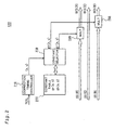
- Fig. 1 is a block diagram schematically illustrating an image display 1000 that is a first embodiment of this invention.
- the image display 1000 comprises a scan converter (SC) 110, a gain corrector 120, a controller 130, a liquid crystal panel driver 150, liquid crystal panels 160, an illumination optical system 170 and a projection optical system 180.
- the image display 1000 is a projector which displays images by projecting red, green and yellow light exiting from the liquid crystal panels 160 at every pixel onto a projection screen SR through the projection optical system 180.
- the structures of the liquid crystal panel 160, illumination optical system 170 and projection optical system 180 are described in assignee's Japanese Patent Laid-Open Gazette No. 10-171045 , the disclosure of which is incorporated herein by reference for all purposes.
- the controller 130 is connected to the SC 110 and the gain corrector 120 through a bus 140.
- the controller 130 sets the processing conditions of the different sections and directly controls the processing of every section.
- the SC 110 outputs a timing signal TCTL used to form an image on the liquid crystal panel 160.
- the timing signal TCTL ordinarily includes a vertical synchronizing signal VD, a horizontal synchronizing signal HD and a clock signal DCLK.
- the SC 110 also outputs a given image signal VS as an image signal DS in a form suitable for input to the liquid crystal panel 160.
- the image data composing the image signal DS include one 24-bit data set for each pixel.
- the data sets are output serially pixel by pixel.
- the image data set of each pixel consists of 8 bits of color data for each of red, green and blue.
- image data contained in the image signal DS will hereafter sometimes be referred to as "image data DS.”
- the gain corrector 120 subjects the image signal DS received from the SC 110 to gain correction in accordance with the positions of the pixels.
- the gain-corrected image data DCS is supplied to the liquid crystal panel driver 150.
- the liquid crystal panel driver 150 supplies the image data DCS to the liquid crystal panel 160 under timing control by the timing signal TCTL.
- the liquid crystal panel 160 modulates illumination light from the illumination optical system 170 in accordance with the supplied image data DCS.
- the projection optical system 180 projects the light modulated by the liquid crystal panel 160 onto the projection screen SR, thereby displaying an image.
- the liquid crystal panel 160 thus corresponds to the image display device of the present invention, while the SC 110 corresponds to the image processor of the invention and the gain corrector 120 corresponds to the gain corrector of the invention.
- Fig. 2 is a block diagram schematically illustrating the gain corrector 120.
- the gain corrector 120 comprises a correction timing controller 210, a constant table 220, a constant selector 230, a red multiplier 240 and a blue multiplier 250.
- the constant table 220 stores red and blue correction gains gr(x, y) and gb(x, y) for each pixel. As shown in Fig.
- the position of each pixel of the liquid crystal panel which comprises multiple pixels in a matrix array, is defined by the value of (x, y) in an orthogonal coordinate system whose origin (0, 0) is defined as the pixel at the left edge in the horizontal direction and the upper edge in the vertical direction; x represents position in the horizontal direction and y position in the vertical direction.
- the correction timing controller 210 uses the given timing signal TCTL to calculate the position (x, y) of the pixel to which the image data DS received from the SC 110 is to be applied.
- the constant selector 230 selects the correction gains gr(x, y), gb(x, y) corresponding to the calculated pixel position (x, y) from the constant table 220 and supplies the red correction gain gr (x, y) to the red multiplier 240 and the correction gain gb(x, y) to blue multiplier 250.
- the red multiplier 240 multiplies the input red image data DS(R) by gr(x, y) and outputs the product as red image data DCS(R).
- the blue multiplier 250 multiplies the input blue image data DS(B) by gb(x, y) and outputs the product as blue image data DCS(B).
- the green image data DS(G) is output unchanged as image data DCS(G).
- the image display 1000 since the image represented by the image data DCS corrected by the gain corrector 120 is formed on the liquid crystal panel 160, the color unevenness that tends to arise in the displayed image can be suppressed as explained in the following.
- Figs. 3(A) and 3(B) illustrate methods of color unevenness correction.
- the levels of the color image data are defined as falling between 0 and 100.
- the red luminance level range is defined as 0Kr to 100Kr
- the green luminance level range as 0Kg to 100Kg
- the blue luminance level range as 0Kb to 100Kb.
- the coefficients Kr, Kg and Kb indicate the contribution of the light of the color concerned to the luminance of light exiting from the pixels. Their values are Kr ⁇ 0.299, Kg ⁇ 0.587 and Kb ⁇ 0.114. If red, green and blue each has an image data level of 50, representing a gray image, the red, green and blue luminance levels of the image to be displayed are defined as 50Kr, 50Kg and 50Kb.
- Fig. 3(A) illustrates occurrence of color unevenness in the case of applying the pixels with gray image data, i.e., image data in which each of red, green and blue has a level of 50.
- the red, green and blue luminance levels at pixel P1 are 50Kr, 50Kg and 50Kb, which are the color luminance levels that should be displayed, but at pixel P2 the luminance level of red is 40Kr, the luminance level of green is 45Kg, and the luminance level of blue is 55Kb, because of the characteristics of the pixel P2. Color unevenness is therefore present.
- luminance levels disregarding the coefficients, (hereafter referred to simply as “luminance levels”) are corrected to 50 for all colors.
- luminance levels are corrected to 50 for all colors.
- Method 1 can correct the luminance level of each color to its proper value, it can suppress color unevenness. Correction by Method 1 is complicated, however, because the image data sets for all possible colors have to be corrected.
- Method 2 defines the luminance level of green as a reference and effects correction for making the luminance levels of red and blue equal to that of green. Specifically, the red image data set is multiplied by the ratio of the green luminance level to the red luminance level (45/40), and the blue image data set is multiplied by the ratio of the green luminance level to the blue luminance level (45/55), thus making the luminance level of all colors equal to the green luminance level of 45.
- Hue and saturation of each color can be defined by chromaticity. In suppressing color unevenness, therefore, it suffices to make the chromaticity of the pixels experiencing color unevenness equal to the proper chromaticity. Taking only chromaticity into consideration, one can see that among lights differing in luminance there exist ones that are the same in chromaticity. For instance, the chromaticity of light whose individual colors have a luminance of 50 and the chromaticity of light whose individual colors have a luminance of 45 are in principle the same and the two lights are displayed as the same color, notwithstanding that they differ in luminance.
- Method 2 suppresses color unevenness by effecting correction of the image data applied to the pixels so that, when an image of uniform color is displayed, all pixels are made equal in color irrespective of change in luminance level.
- Method 2 may result in luminance scatter (luminance unevenness), it can achieve the same suppression of color unevenness as Method 1.
- Method 2 requires correction of only two color data sets and is therefore advantageous to Method 1 in ease of correction.
- Method 2 can be implemented using a gain corrector that is structurally simpler than would be needed for implementing Method 2.
- Method 2 may produce luminance unevenness. As explained in the following, however, this is not a problem in practical application.
- the human eye is less sensitive to luminance unevenness than color unevenness. Further, while it is somewhat sensitive to changes in the luminance level of light from nearby sources, it is insensitive to changes in the luminance level of light from relatively distant sources. As color unevenness generally has a rather gradual distribution, the luminance unevenness caused by the changes in luminance produced when color unevenness is suppressed by Method 2 therefore also has a rather gradual distribution. Luminance unevenness is therefore not strongly perceived. Furthermore, as was pointed out earlier, the rates at which red, green and blue contribute to the luminance of the light exiting from the pixels are Kr ⁇ 0.299, Kg ⁇ 0.587 and Kb ⁇ 0.114, with the contribution of green being the greatest. Since Method 2 defines green, the color making the largest contribution to luminance, as the reference, it holds the effect of luminance change to the very minimum. For the foregoing reasons, luminance unevenness produced by Method 2 causes substantially no problem in practical application.
- Method 2 was explained with regard to the case of adjusting the luminance levels of red and blue light to the luminance level of green light but either red or blue can be used the reference instead. Still, in view of the fact that green has the greatest effect on luminance among the three colors, green is preferably adopted as the reference. In a case where color images are formed using a combination of colors other than the three primary colors (red, green and blue), the same effects can be obtained by selecting one of the colors as a reference, particularly by selecting the color among them that has the greatest effect on luminance.
- the correction gains gr(x, y) and gb(x, y) stored in the constant table 220 correspond to the ratio of pixel green luminance level to red luminance level and the ratio of pixel green luminance level to blue luminance level in Method 2.
- the gains are determined in the following manner:
- the procedure for determining the correction gains is not limited to the steps i) to iii) set out above.
- an image of a color other than gray can be displayed instead of the uniform gray image.
- the image should preferable be of a color including red, green blue.
- the chromaticity of every pixel is measured in ii)
- the procedure is not limited to this.
- Any procedure can be adopted that, during display of an image of uniform color, enables the correction gains of every pixel to be determined so as to reduce any difference between the chromaticity of the pixel and the chromaticity of the color desired to be displayed.
- the image display 1000 is configured so that, during display of an image of uniform color, the image data supplied to the liquid crystal panel 160 can be corrected in the gain corrector 120 so that the light exiting from every pixel is made to have the same chromaticity. It can therefore suppress color unevenness.
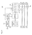
- Fig. 4 is a block diagram schematically illustrating a gain corrector 120A of a second embodiment of this invention.
- An image display similar to that of the first embodiment can be configured by replacing the gain corrector 120 of the first embodiment with this gain corrector 120A.
- the gain corrector 120A comprises a correction timing controller 210, a constant table 220A, a constant selector 230, a red multiplier 240, a blue multiplier 250, an area detector 260 and a gain calculator 270.
- the area detector 260 detects a segment (hereinafter called an "area” or “plane”) that includes the pixel position (x, y) calculated by the correction timing controller 210.
- area a segment that includes the pixel position (x, y) calculated by the correction timing controller 210.
- area a segment that includes the pixel position (x, y) calculated by the correction timing controller 210.
- the meaning of "area” will be explained with reference to Fig. 5 .
- designate those at the four corners as PA, PC, PG and PI designate the center pixel as PE, designate the pixels at the left and right ends of the horizontal line passing through the center pixel PE as PD and PF, and designate the pixels at the upper and lower ends of the vertical line passing through the center pixel PE as PB and PH.
- the positions of the pixels PB, PC, PD, PE, PF, PG, PH are PI are defined as (XB, 0), (XC, 0), (0, YD), (XB, YD), (XC, YD), (0, YG), (XB, YG), (XC, YG).
- the area detector 260 discriminates the area in which the pixel position (x, y) given by the correction timing controller 210 is present. The method of this discrimination will now be explained. As can be seen in Fig. 5 , the pixel belongs to an area in the right half when x ⁇ XB and to an area in the left half when x ⁇ XB. Further, the pixel belongs to an area in the lower half when y ⁇ YD and to an area in the upper half when y ⁇ YD.
- the area detector 260 discriminates that the area in which the pixel position (x, y) given by the correction timing controller 210 is present is the first or second area when x ⁇ XB and y ⁇ YD, is the third or fourth area when x ⁇ XB and y ⁇ YD, is the fifth or sixth area when x ⁇ XB and y ⁇ YD, and is the seventh or eighth area when x ⁇ XB and y ⁇ YD.
- Figs. 6(A) and 6(B) show conditions used to discriminate whether the area in which the pixel position (x, y) given by the correction timing controller 210 is present is the first area or the second area.
- Equation (1) is therefore used to discriminate between the first area and the second area as shown by Equation (2a) and Equation (2b):
- First area y - - Y ⁇ 01 / X ⁇ 01 • x + Y ⁇ 01 ⁇ 0
- Second area y - - Y ⁇ 01 / X ⁇ 01 • x + Y ⁇ 01 ⁇ 0
- pixel PB is defined as the origin (0, 0).
- Equation (3) is therefore used to discriminate between the third area and the fourth area as shown by Equation (4a) and Equation (4b):
- Third area y - Y ⁇ 02 / X ⁇ 02 • x ⁇ 0
- Fourth area y - Y ⁇ 02 / X ⁇ 02 • x ⁇ 0
- Discrimination between the fifth area and the sixth area is carried out similarly to that between the third area and the fourth area while the pixel PD is used as the origin (0, 0).
- the discrimination is then made as shown by Equation (5a) and Equation (5b): Fifth area : y - Y ⁇ 03 / X ⁇ 03 • x ⁇ 0
- Sixth area : y - Y ⁇ 03 / X ⁇ 03 • x ⁇ 0
- pixel PE is defined as the origin (0, 0).
- the area detector 260 can thus detect the area including the pixel to be corrected in the foregoing manner.
- the constant selector 230 receives the area data PLS indicating the area discriminated by the area detector 260, selects the corresponding constants ar i , br i , cri, ab i , bb i and cb i from the constant table 220A, and supplies them to the gain calculator 270.
- the gain calculator 270 determines the correction gain for every pixel in the discriminated area (segment pixel) by linear interpolation from the correction gains of the pixels at the area apexes (apex pixels).
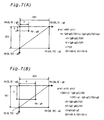
- Figs. 7(A) and 7(B) show the gain calculation for pixels present in the first and second areas conducted in the gain calculator 270.
- the correction gains of the apex pixels PA, PB and PD can be obtained in advance using the correction gain determining procedure explained with regard to the first embodiment.
- the correction gains of the segment pixels in the other areas can also be determined by interpolation from the correction gains of the apex pixels of the area, similarly to what was explained with regard to the first and second areas.
- Fig. 8 is diagram showing examples of correction gain interpolation equations and constants stored in the constant table 220A for the respective areas.
- the interpolation equations and constants shown in Fig. 8 are non-limitative examples. They can be replaced by any of various other interpolation equations and constants usable for interpolating the correction gains of the segment pixels from the apex pixels of the respective areas.
- the gain calculator 270 thus determines the correction gains gr and gb for every pixel and supplies them to the red multiplier 240 and the blue multiplier 250.
- the gain corrector 120A corrects given image data DS(R), DS(G) and DS(B) and outputs them as image data DCS(R), DCS(G) and DCS(B).
- the image represented by the image data DCS corrected by the gain corrector 120A is formed on the liquid crystal panel 160. As a result, an image suppressed in color unevenness is displayed.
- the gain corrector 120A corrects the red and blue image data among the image data of every pixel so as to make their levels substantially equal to the level of the green image data.
- the color unevenness tending to occur in the displayed image can therefore be suppressed.
- the pixels are divided into multiple areas beforehand and the correction gain of any given pixel present in an area is determined by interpolation from the correction gains of the apex pixels of the area. This is advantageous in not requiring the correction gains of all pixels to be calculated in advance. It is also advantageous in that it simplifies the procedure for determining the correction gains in advance and reduces the size of the constant table for storing data corresponding to the determined correction gains.
- the second embodiment defines the eight areas using the vertical line connecting pixels PB, PE and PH, the horizontal line connecting the pixels PD, PE and PF, and the sides of the rhombus having pixels PB, PD, PH and PF as its apexes.
- the distribution of color unevenness is generally such that the unevenness spreads radially outward from the image center toward the image periphery, and the area segmentation of the second embodiment is an example for coping with this distribution.
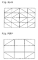
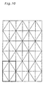
- the invention is not limited to this segmentation. For example, one of the segmentations shown in Figs. 9 and 10 can be adopted.
- the area pattern illustrated in Fig. 10 is what is obtained by using the set of areas of Fig. 5 as a unit for dividing the image horizontally and vertically into multiple identical sets. As this pattern enables the correction processing to be conducted by repeating the same processing for each set, it makes the correction processing easier.
Landscapes
- Engineering & Computer Science (AREA)
- Physics & Mathematics (AREA)
- Computer Hardware Design (AREA)
- General Physics & Mathematics (AREA)
- Theoretical Computer Science (AREA)
- Multimedia (AREA)
- Signal Processing (AREA)
- Control Of Indicators Other Than Cathode Ray Tubes (AREA)
- Liquid Crystal Display Device Control (AREA)
- Video Image Reproduction Devices For Color Tv Systems (AREA)
- Liquid Crystal (AREA)
Applications Claiming Priority (2)
| Application Number | Priority Date | Filing Date | Title |
|---|---|---|---|
| JP17225499A JP3632505B2 (ja) | 1999-06-18 | 1999-06-18 | 画像表示装置 |
| EP00305126A EP1061500B1 (de) | 1999-06-18 | 2000-06-16 | Farbkorrektur in einem Bildanzeigegerät |
Related Parent Applications (1)
| Application Number | Title | Priority Date | Filing Date |
|---|---|---|---|
| EP00305126.5 Division | 2000-06-16 |
Publications (1)
| Publication Number | Publication Date |
|---|---|
| EP2276018A1 true EP2276018A1 (de) | 2011-01-19 |
Family
ID=15938492
Family Applications (2)
| Application Number | Title | Priority Date | Filing Date |
|---|---|---|---|
| EP00305126A Expired - Lifetime EP1061500B1 (de) | 1999-06-18 | 2000-06-16 | Farbkorrektur in einem Bildanzeigegerät |
| EP10010474A Withdrawn EP2276018A1 (de) | 1999-06-18 | 2000-06-16 | Farbkorrektur in einem Bildanzeigegerät |
Family Applications Before (1)
| Application Number | Title | Priority Date | Filing Date |
|---|---|---|---|
| EP00305126A Expired - Lifetime EP1061500B1 (de) | 1999-06-18 | 2000-06-16 | Farbkorrektur in einem Bildanzeigegerät |
Country Status (7)
| Country | Link |
|---|---|
| US (1) | US7050074B1 (de) |
| EP (2) | EP1061500B1 (de) |
| JP (1) | JP3632505B2 (de) |
| KR (1) | KR100481615B1 (de) |
| CN (2) | CN1231805C (de) |
| DE (1) | DE60045203D1 (de) |
| TW (1) | TW484329B (de) |
Families Citing this family (33)
| Publication number | Priority date | Publication date | Assignee | Title |
|---|---|---|---|---|
| CN100365682C (zh) * | 2001-04-26 | 2008-01-30 | 中华映管股份有限公司 | 改善等离子平面显示器上色纯度及色温的补偿方法 |
| CN100356420C (zh) * | 2001-04-26 | 2007-12-19 | 中华映管股份有限公司 | 改善等离子平面显示器上色温及色偏差的补偿方法 |
| US7030846B2 (en) * | 2001-07-10 | 2006-04-18 | Samsung Electronics Co., Ltd. | Color correction liquid crystal display and method of driving same |
| US7253845B2 (en) * | 2002-01-22 | 2007-08-07 | Thomson Licensing | Color non-uniformity correction for LCOS |
| FR2837056B1 (fr) * | 2002-03-07 | 2004-09-17 | France Telecom | Procede et systeme d'uniformisation du rendu colorimetrique d'une juxtaposition de surfaces d'affichage |
| TWI381702B (zh) * | 2003-06-17 | 2013-01-01 | Semiconductor Energy Lab | 具有攝像功能之顯示裝置及雙向通訊系統 |
| KR20050057767A (ko) * | 2003-12-11 | 2005-06-16 | 엘지전자 주식회사 | 해상도 향상 장치 및 방법 그리고 이를 이용한디스플레이장치 |
| JP2005249821A (ja) * | 2004-03-01 | 2005-09-15 | Seiko Epson Corp | 色補正回路及びそれを備えた画像表示装置 |
| CN100397476C (zh) * | 2004-03-12 | 2008-06-25 | 友达光电股份有限公司 | 显示器的色彩补偿电路与其补偿方法 |
| EP1747547B1 (de) * | 2004-05-11 | 2009-07-22 | Nxp B.V. | Verfahren zum verarbeiten von bilddaten |
| JP4196959B2 (ja) * | 2004-05-20 | 2008-12-17 | セイコーエプソン株式会社 | 電気光学装置及びその駆動回路並びに電子機器 |
| US20060007239A1 (en) * | 2004-07-06 | 2006-01-12 | Harrison Charles F | Color correction system |
| KR100794785B1 (ko) * | 2004-07-29 | 2008-01-21 | 삼성전자주식회사 | 자기 기록/재생장치의 헤드드럼 조립체 |
| JP5127121B2 (ja) * | 2004-09-14 | 2013-01-23 | キヤノン株式会社 | 表示装置及び表示方法 |
| EP1650730B1 (de) | 2004-10-25 | 2009-12-30 | Barco NV | Optische Korrektur für Leuchtpaneele mit hoher Gleichmäßigkeit |
| JP5134768B2 (ja) * | 2005-05-19 | 2013-01-30 | 株式会社ジャパンディスプレイイースト | 画像表示装置 |
| JP2007025635A (ja) * | 2005-06-17 | 2007-02-01 | Fujitsu Hitachi Plasma Display Ltd | プラズマディスプレイ装置及びその処理方法 |
| KR100809343B1 (ko) * | 2005-11-07 | 2008-03-05 | 삼성전자주식회사 | 디스플레이 장치 화면의 공간적 불균일을 보정하는 방법 및장치 |
| US7564438B2 (en) * | 2006-03-24 | 2009-07-21 | Marketech International Corp. | Method to automatically regulate brightness of liquid crystal displays |
| JP4207064B2 (ja) * | 2006-07-25 | 2009-01-14 | セイコーエプソン株式会社 | 電気光学装置、画像処理回路、画像処理方法、及び電子機器 |
| JP4222392B2 (ja) | 2006-08-04 | 2009-02-12 | セイコーエプソン株式会社 | 画像表示装置および画像表示方法 |
| TWI354492B (en) * | 2007-03-07 | 2011-12-11 | Marketech Int Corp | Image processing apparatus |
| KR101097639B1 (ko) * | 2008-10-20 | 2011-12-22 | 파나소닉 주식회사 | 화상 표시 장치, 색 신호 보정 장치 및 색 신호 보정 방법 |
| TWI404034B (zh) * | 2009-01-23 | 2013-08-01 | Mstar Semiconductor Inc | 過驅動值產生裝置及過驅動值產生方法 |
| CN101815158B (zh) * | 2009-02-20 | 2012-07-04 | 华晶科技股份有限公司 | 改善数字影像中色影的补偿方法 |
| KR101319352B1 (ko) * | 2009-12-11 | 2013-10-16 | 엘지디스플레이 주식회사 | 액정 표시 장치의 로컬 디밍 구동 방법 및 장치 |
| WO2012073338A1 (ja) * | 2010-11-30 | 2012-06-07 | Necディスプレイソリューションズ株式会社 | 表示装置、表示装置の色補正方法 |
| DE102013206832A1 (de) * | 2013-04-16 | 2014-10-16 | Robert Bosch Gmbh | Bilddarstellungsvorrichtung, mobiltelefon und verfahren |
| WO2015152923A1 (en) * | 2014-04-03 | 2015-10-08 | Empire Technology Development Llc | Color smear correction based on inertial measurements |
| CN108022565B (zh) * | 2016-11-02 | 2021-03-30 | 群创光电股份有限公司 | 调整方法以及显示器 |
| US10685607B2 (en) * | 2016-11-02 | 2020-06-16 | Innolux Corporation | Adjustment method for display de-Mura |
| KR102692179B1 (ko) * | 2019-12-26 | 2024-08-06 | 주식회사 엘엑스세미콘 | 무라 보상 회로 및 그를 채용한 디스플레이를 위한 구동 장치 |
| CN113889028A (zh) * | 2021-09-23 | 2022-01-04 | 惠州市艾比森光电有限公司 | 显示屏箱体的校正方法及装置 |
Citations (3)
| Publication number | Priority date | Publication date | Assignee | Title |
|---|---|---|---|---|
| EP0402137A2 (de) * | 1989-06-08 | 1990-12-12 | Matsushita Electric Industrial Co., Ltd. | Projektionsbildanzeigevorrichtung |
| US5359342A (en) * | 1989-06-15 | 1994-10-25 | Matsushita Electric Industrial Co., Ltd. | Video signal compensation apparatus |
| JPH10171045A (ja) | 1996-12-10 | 1998-06-26 | Seiko Epson Corp | 投写型表示装置 |
Family Cites Families (19)
| Publication number | Priority date | Publication date | Assignee | Title |
|---|---|---|---|---|
| US5293224A (en) * | 1990-01-30 | 1994-03-08 | Pioneer Electronic Corporation | White balance control system |
| US5047861A (en) * | 1990-07-31 | 1991-09-10 | Eastman Kodak Company | Method and apparatus for pixel non-uniformity correction |
| US5289286A (en) * | 1991-07-18 | 1994-02-22 | Minolta Camera Kabushiki Kaisha | Solid state sensor having logarithmic photovoltaic response, with pixel uniformity correction and white balance circuitry therefor |
| JPH05197357A (ja) * | 1992-01-22 | 1993-08-06 | Matsushita Electric Ind Co Ltd | 画像表示装置 |
| JPH06138849A (ja) * | 1992-10-30 | 1994-05-20 | Sharp Corp | 液晶映像表示装置 |
| JP3014895B2 (ja) * | 1993-06-02 | 2000-02-28 | 株式会社日立製作所 | ビデオカメラ |
| US6081254A (en) * | 1993-08-12 | 2000-06-27 | Hitachi, Ltd. | Color correction system of imaging apparatus |
| JP3672586B2 (ja) * | 1994-03-24 | 2005-07-20 | 株式会社半導体エネルギー研究所 | 補正システムおよびその動作方法 |
| US5510851A (en) * | 1994-03-29 | 1996-04-23 | Radius Inc. | Method and apparatus for dynamic purity correction |
| US5483259A (en) * | 1994-04-12 | 1996-01-09 | Digital Light & Color Inc. | Color calibration of display devices |
| US5883476A (en) * | 1994-06-09 | 1999-03-16 | Hitachi, Ltd. | Convergence correction system with recovery function and display apparatus using the same |
| JPH0865546A (ja) * | 1994-08-18 | 1996-03-08 | Fuji Photo Film Co Ltd | シェーディング補正係数生成回路およびシェーディング補正係数生成方法 |
| US5452109A (en) * | 1994-08-31 | 1995-09-19 | Eastman Kodak Company | Digital image signal processing apparatus and method for accumulating blocks of signal data from an imager |
| CN1070013C (zh) * | 1994-12-14 | 2001-08-22 | 松下电器产业株式会社 | 具有校正亮度不均匀性的电路的投影型图像显示装置 |
| US5539459A (en) * | 1995-05-18 | 1996-07-23 | Polaroid Corporation | Optimal tone scale mapping in electronic cameras |
| KR970058038A (ko) * | 1995-12-08 | 1997-07-31 | 배순훈 | 휘도 변화에 따른 색좌표 보정 장치 및 그 제어 방법 |
| US6043797A (en) * | 1996-11-05 | 2000-03-28 | Clarity Visual Systems, Inc. | Color and luminance control system for liquid crystal projection displays |
| JP3719317B2 (ja) * | 1997-09-30 | 2005-11-24 | ソニー株式会社 | 補間方法、補間回路、画像表示装置 |
| JP2001209358A (ja) * | 2000-01-26 | 2001-08-03 | Seiko Epson Corp | 表示画像のムラ補正 |
-
1999
- 1999-06-18 JP JP17225499A patent/JP3632505B2/ja not_active Expired - Fee Related
-
2000
- 2000-06-07 KR KR10-2000-0031003A patent/KR100481615B1/ko not_active Expired - Fee Related
- 2000-06-08 TW TW089111122A patent/TW484329B/zh not_active IP Right Cessation
- 2000-06-13 US US09/592,734 patent/US7050074B1/en not_active Expired - Lifetime
- 2000-06-16 DE DE60045203T patent/DE60045203D1/de not_active Expired - Lifetime
- 2000-06-16 EP EP00305126A patent/EP1061500B1/de not_active Expired - Lifetime
- 2000-06-16 EP EP10010474A patent/EP2276018A1/de not_active Withdrawn
- 2000-06-19 CN CNB2003101015773A patent/CN1231805C/zh not_active Expired - Fee Related
- 2000-06-19 CN CN00118640A patent/CN1130584C/zh not_active Expired - Fee Related
Patent Citations (3)
| Publication number | Priority date | Publication date | Assignee | Title |
|---|---|---|---|---|
| EP0402137A2 (de) * | 1989-06-08 | 1990-12-12 | Matsushita Electric Industrial Co., Ltd. | Projektionsbildanzeigevorrichtung |
| US5359342A (en) * | 1989-06-15 | 1994-10-25 | Matsushita Electric Industrial Co., Ltd. | Video signal compensation apparatus |
| JPH10171045A (ja) | 1996-12-10 | 1998-06-26 | Seiko Epson Corp | 投写型表示装置 |
Also Published As
| Publication number | Publication date |
|---|---|
| JP3632505B2 (ja) | 2005-03-23 |
| KR20010007266A (ko) | 2001-01-26 |
| CN1130584C (zh) | 2003-12-10 |
| JP2001008219A (ja) | 2001-01-12 |
| EP1061500A2 (de) | 2000-12-20 |
| EP1061500A3 (de) | 2002-05-02 |
| CN1281153A (zh) | 2001-01-24 |
| US7050074B1 (en) | 2006-05-23 |
| EP1061500B1 (de) | 2010-11-10 |
| DE60045203D1 (de) | 2010-12-23 |
| CN1512249A (zh) | 2004-07-14 |
| CN1231805C (zh) | 2005-12-14 |
| TW484329B (en) | 2002-04-21 |
| KR100481615B1 (ko) | 2005-04-08 |
Similar Documents
| Publication | Publication Date | Title |
|---|---|---|
| EP1061500B1 (de) | Farbkorrektur in einem Bildanzeigegerät | |
| US6704008B2 (en) | Non-uniformity correction for displayed images | |
| JP3719317B2 (ja) | 補間方法、補間回路、画像表示装置 | |
| JP3766672B2 (ja) | 画像補正データ算出方法 | |
| RU2471214C2 (ru) | Устройство управления жидкокристаллическим дисплеем, жидкокристаллический дисплей, способ управления жидкокристаллическим дисплеем, программа и носитель данных | |
| NL1029261C2 (nl) | Inrichting en werkwijze voor het bewerken van een kleurensignaal. | |
| EP1478192B1 (de) | Bildverarbeitungssystem, Projektor, Informationsspeichermedium und Bildverarbeitungsverfahren | |
| US20090213337A1 (en) | Image projecting system, method, computer program and recording medium | |
| US7978201B2 (en) | Method for compensating an image | |
| CN101822043B (zh) | 图像显示设备 | |
| US20080036872A1 (en) | Image processing system, display device, program, and information recording medium | |
| JP2010057149A (ja) | 画像補正データ生成システム、画像補正データ生成方法、画像補正データ生成プログラム及び画像補正回路 | |
| CN104505021B (zh) | 像素显示调整方法及装置 | |
| CN115985269A (zh) | 亮度补偿方法及装置、计算机可读存储介质 | |
| US20120218283A1 (en) | Method for Obtaining Brighter Images from an LED Projector | |
| US8422812B2 (en) | Image processor and method therefor, and image display device | |
| US20090213335A1 (en) | Image projecting system, image projecting method, computer program, and recording medium | |
| JP3760117B2 (ja) | 画像信号処理装置、画像表示装置、マルチディスプレイ装置及び当該マルチディスプレイ装置における色度調整方法 | |
| EP2161918B1 (de) | Bildprozessor, Bildanzeigevorrichtung, Bildverarbeitungsverfahren und Bildanzeigeverfahren | |
| JP4583863B2 (ja) | 画像表示システム | |
| US20060007239A1 (en) | Color correction system | |
| US7002606B2 (en) | Image signal processing apparatus, image display apparatus, multidisplay apparatus, and chromaticity adjustment method for use in the multidisplay apparatus | |
| EP1760688A2 (de) | Verfahren zur Erzeugung einer Gammakurve und Vorrichtung dafür | |
| JP3515042B2 (ja) | 画像表示装置および画像信号補正装置 | |
| US20130249780A1 (en) | Projection display and lack of brightness uniformity compensation method |
Legal Events
| Date | Code | Title | Description |
|---|---|---|---|
| PUAI | Public reference made under article 153(3) epc to a published international application that has entered the european phase |
Free format text: ORIGINAL CODE: 0009012 |
|
| 17P | Request for examination filed |
Effective date: 20101011 |
|
| AC | Divisional application: reference to earlier application |
Ref document number: 1061500 Country of ref document: EP Kind code of ref document: P |
|
| AK | Designated contracting states |
Kind code of ref document: A1 Designated state(s): DE FR GB |
|
| STAA | Information on the status of an ep patent application or granted ep patent |
Free format text: STATUS: THE APPLICATION HAS BEEN WITHDRAWN |
|
| 18W | Application withdrawn |
Effective date: 20130222 |