EP2276049A1 - Écran plasma - Google Patents
Écran plasma Download PDFInfo
- Publication number
- EP2276049A1 EP2276049A1 EP09700053A EP09700053A EP2276049A1 EP 2276049 A1 EP2276049 A1 EP 2276049A1 EP 09700053 A EP09700053 A EP 09700053A EP 09700053 A EP09700053 A EP 09700053A EP 2276049 A1 EP2276049 A1 EP 2276049A1
- Authority
- EP
- European Patent Office
- Prior art keywords
- dielectric layer
- oxide
- aggregated particles
- aggregated
- protective layer
- Prior art date
- Legal status (The legal status is an assumption and is not a legal conclusion. Google has not performed a legal analysis and makes no representation as to the accuracy of the status listed.)
- Withdrawn
Links
Images



Classifications
-
- H—ELECTRICITY
- H01—ELECTRIC ELEMENTS
- H01J—ELECTRIC DISCHARGE TUBES OR DISCHARGE LAMPS
- H01J11/00—Gas-filled discharge tubes with alternating current induction of the discharge, e.g. alternating current plasma display panels [AC-PDP]; Gas-filled discharge tubes without any main electrode inside the vessel; Gas-filled discharge tubes with at least one main electrode outside the vessel
- H01J11/20—Constructional details
- H01J11/34—Vessels, containers or parts thereof, e.g. substrates
- H01J11/40—Layers for protecting or enhancing the electron emission, e.g. MgO layers
-
- H—ELECTRICITY
- H01—ELECTRIC ELEMENTS
- H01J—ELECTRIC DISCHARGE TUBES OR DISCHARGE LAMPS
- H01J11/00—Gas-filled discharge tubes with alternating current induction of the discharge, e.g. alternating current plasma display panels [AC-PDP]; Gas-filled discharge tubes without any main electrode inside the vessel; Gas-filled discharge tubes with at least one main electrode outside the vessel
- H01J11/10—AC-PDPs with at least one main electrode being out of contact with the plasma
- H01J11/12—AC-PDPs with at least one main electrode being out of contact with the plasma with main electrodes provided on both sides of the discharge space
-
- H—ELECTRICITY
- H01—ELECTRIC ELEMENTS
- H01J—ELECTRIC DISCHARGE TUBES OR DISCHARGE LAMPS
- H01J11/00—Gas-filled discharge tubes with alternating current induction of the discharge, e.g. alternating current plasma display panels [AC-PDP]; Gas-filled discharge tubes without any main electrode inside the vessel; Gas-filled discharge tubes with at least one main electrode outside the vessel
- H01J11/20—Constructional details
- H01J11/34—Vessels, containers or parts thereof, e.g. substrates
Definitions
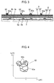
- Fig. 2 is a sectional view showing a configuration of front panel 2 of PDP 1 in accordance with the exemplary embodiment of the present invention.
- Fig. 2 is shown turned upside down with respect to Fig. 1 .
- display electrodes 6 each composed of scan electrode 4 and sustain electrode 5 and light blocking layers 7 are pattern-formed on front glass substrate 3 produced by, for example, a float method.
- Scan electrode 4 and sustain electrode 5 include transparent electrodes 4a and 5a made of indium tin oxide (ITO), tin oxide (SnO 2 ), or the like, and metal bus electrodes 4b and 5b formed on transparent electrodes 4a and 5a, respectively.
- Metal bus electrodes 4b and 5b are used for the purpose of providing the conductivity in the longitudinal direction of transparent electrodes 4a and 5a and formed of a conductive material containing a silver (Ag) material as a main component.
- a dielectric material of second dielectric layer 82 includes the following material compositions: 11 wt.% to 20 wt.% of bismuth oxide (Bi 2 O 3 ); furthermore, 1.6 wt.% to 21 wt.% of at least one selected from calcium oxide (CaO), strontium oxide (SrO), and barium oxide (BaO); and 0.1 wt.% to 7 wt.% of at least one selected from molybdenum oxide (MoO 3 ), tungsten oxide (WO 3 ), and cerium oxide (CeO 2 ).
- MoO 3 molybdenum oxide
- WO 3 tungsten oxide
- CeO 2 cerium oxide
- MoO 3 molybdenum oxide
- tungsten oxide WO 3
- cerium oxide CeO 2
- 0.1 wt.% to 7 wt.% of at least one selected from copper oxide (CuO), chromium oxide (Cr 2 O 3 ), cobalt oxide (Co 2 O 3 ), vanadium oxide (V 2 O 7 ), antimony oxide (Sb 2 O 3 ) and manganese oxide (MnO 2 ) may be included.
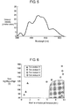
- Fig. 11 is a graph showing one example of the particle size distribution of the aggregated particles in the PDP in accordance with the exemplary embodiment of the present invention.
- the frequency (%) shown in the ordinate is a rate (%) of the amount of aggregated particles existing in each of divided ranges of particle diameters shown in the abscissas with respect to the total amount.
- Fig. 11 it is shown that by using aggregated particles having an average particle diameter that is in the range of not less than 0.9 ⁇ m and not more than 2 ⁇ m, the above-mentioned effect of the present invention can be obtained stably.
Landscapes
- Physics & Mathematics (AREA)
- Engineering & Computer Science (AREA)
- Plasma & Fusion (AREA)
- Gas-Filled Discharge Tubes (AREA)
Applications Claiming Priority (2)
| Application Number | Priority Date | Filing Date | Title |
|---|---|---|---|
| JP2008058935A JP2009218027A (ja) | 2008-03-10 | 2008-03-10 | プラズマディスプレイパネル |
| PCT/JP2009/000299 WO2009113230A1 (fr) | 2008-03-10 | 2009-01-27 | Écran plasma |
Publications (2)
| Publication Number | Publication Date |
|---|---|
| EP2276049A1 true EP2276049A1 (fr) | 2011-01-19 |
| EP2276049A4 EP2276049A4 (fr) | 2011-04-20 |
Family
ID=41064904
Family Applications (1)
| Application Number | Title | Priority Date | Filing Date |
|---|---|---|---|
| EP09700053A Withdrawn EP2276049A4 (fr) | 2008-03-10 | 2009-01-27 | Écran plasma |
Country Status (6)
| Country | Link |
|---|---|
| US (1) | US8198813B2 (fr) |
| EP (1) | EP2276049A4 (fr) |
| JP (1) | JP2009218027A (fr) |
| KR (1) | KR101151135B1 (fr) |
| CN (1) | CN101681767B (fr) |
| WO (1) | WO2009113230A1 (fr) |
Families Citing this family (1)
| Publication number | Priority date | Publication date | Assignee | Title |
|---|---|---|---|---|
| JP2009129617A (ja) * | 2007-11-21 | 2009-06-11 | Panasonic Corp | プラズマディスプレイパネル |
Family Cites Families (18)
| Publication number | Priority date | Publication date | Assignee | Title |
|---|---|---|---|---|
| US7348729B2 (en) * | 2000-08-29 | 2008-03-25 | Matsushita Electric Industrial Co., Ltd. | Plasma display panel and production method thereof and plasma display panel display unit |
| JP2002110050A (ja) * | 2000-09-29 | 2002-04-12 | Hitachi Ltd | プラズマ表示パネル |
| JP4654520B2 (ja) * | 2001-02-06 | 2011-03-23 | パナソニック株式会社 | プラズマディスプレイパネルおよびその製造方法 |
| JP4225761B2 (ja) * | 2002-10-10 | 2009-02-18 | 三菱マテリアル株式会社 | Si濃度を調整した多結晶MgO蒸着材 |
| US7102287B2 (en) * | 2002-11-18 | 2006-09-05 | Matsushita Electric Industrial Co., Ltd. | Plasma display panel and manufacturing method therefor |
| JP4611207B2 (ja) * | 2003-11-10 | 2011-01-12 | パナソニック株式会社 | プラズマディスプレイパネル |
| JP4399344B2 (ja) * | 2004-11-22 | 2010-01-13 | パナソニック株式会社 | プラズマディスプレイパネルおよびその製造方法 |
| JP4611057B2 (ja) * | 2005-03-01 | 2011-01-12 | 宇部マテリアルズ株式会社 | 交流型プラズマディスプレイパネルの誘電体層保護膜形成用の酸化マグネシウム微粒子分散液 |
| JP4839937B2 (ja) | 2005-07-14 | 2011-12-21 | パナソニック株式会社 | 酸化マグネシウム原材料およびプラズマディスプレイパネルの製造方法 |
| JP2007184264A (ja) | 2006-01-04 | 2007-07-19 | Lg Electronics Inc | プラズマディスプレイパネル及びその製造方法 |
| JP4476334B2 (ja) | 2006-04-28 | 2010-06-09 | パナソニック株式会社 | プラズマディスプレイパネルとその製造方法 |
| WO2007126061A1 (fr) * | 2006-04-28 | 2007-11-08 | Panasonic Corporation | Ecran a plasma et son procede de fabrication |
| JP4774329B2 (ja) * | 2006-05-16 | 2011-09-14 | パナソニック株式会社 | プラズマディスプレイパネル |
| KR20090049562A (ko) * | 2006-08-21 | 2009-05-18 | 아사히 가라스 가부시키가이샤 | 플라즈마 디스플레이 패널 및 그 제조 방법 |
| JP4542080B2 (ja) * | 2006-11-10 | 2010-09-08 | パナソニック株式会社 | プラズマディスプレイパネル及びその製造方法 |
| US20080157673A1 (en) * | 2006-12-28 | 2008-07-03 | Yusuke Fukui | Plasma display panel and manufacturing method therefor |
| JP2008293772A (ja) | 2007-05-24 | 2008-12-04 | Panasonic Corp | プラズマディスプレイパネル及びその製造方法、並びにプラズマディスプレイパネル |
| JP2009170192A (ja) | 2008-01-15 | 2009-07-30 | Panasonic Corp | プラズマディスプレイパネル |
-
2008
- 2008-03-10 JP JP2008058935A patent/JP2009218027A/ja active Pending
-
2009
- 2009-01-27 WO PCT/JP2009/000299 patent/WO2009113230A1/fr not_active Ceased
- 2009-01-27 KR KR1020097016775A patent/KR101151135B1/ko not_active Expired - Fee Related
- 2009-01-27 CN CN2009800001961A patent/CN101681767B/zh not_active Expired - Fee Related
- 2009-01-27 EP EP09700053A patent/EP2276049A4/fr not_active Withdrawn
- 2009-01-27 US US12/595,712 patent/US8198813B2/en not_active Expired - Fee Related
Also Published As
| Publication number | Publication date |
|---|---|
| JP2009218027A (ja) | 2009-09-24 |
| CN101681767A (zh) | 2010-03-24 |
| EP2276049A4 (fr) | 2011-04-20 |
| US20100127622A1 (en) | 2010-05-27 |
| KR101151135B1 (ko) | 2012-06-01 |
| CN101681767B (zh) | 2011-06-01 |
| KR20090116741A (ko) | 2009-11-11 |
| US8198813B2 (en) | 2012-06-12 |
| WO2009113230A1 (fr) | 2009-09-17 |
Similar Documents
| Publication | Publication Date | Title |
|---|---|---|
| EP2214193B1 (fr) | Écran d'affichage à plasma | |
| US8395320B2 (en) | Plasma display panel | |
| EP2101342A1 (fr) | Écran d'affichage à plasma | |
| EP2099051B1 (fr) | Écran d'affichage à plasma | |
| EP2120251A1 (fr) | Écran à plasma | |
| US8143786B2 (en) | Plasma display panel | |
| EP2124241B1 (fr) | Écran plasma | |
| US7994718B2 (en) | Plasma display panel | |
| EP2099049A1 (fr) | Procédé de fabrication d'un écran d'affichage à plasma | |
| US8198813B2 (en) | Plasma display panel | |
| US8053989B2 (en) | Plasma display panel | |
| US8164262B2 (en) | Plasma display panel | |
| EP2141726B1 (fr) | Écran plasma | |
| EP2141727A1 (fr) | Panneau d'affichage à plasma |
Legal Events
| Date | Code | Title | Description |
|---|---|---|---|
| PUAI | Public reference made under article 153(3) epc to a published international application that has entered the european phase |
Free format text: ORIGINAL CODE: 0009012 |
|
| 17P | Request for examination filed |
Effective date: 20090612 |
|
| AK | Designated contracting states |
Kind code of ref document: A1 Designated state(s): AT BE BG CH CY CZ DE DK EE ES FI FR GB GR HR HU IE IS IT LI LT LU LV MC MK MT NL NO PL PT RO SE SI SK TR |
|
| AX | Request for extension of the european patent |
Extension state: AL BA RS |
|
| A4 | Supplementary search report drawn up and despatched |
Effective date: 20110322 |
|
| DAX | Request for extension of the european patent (deleted) | ||
| STAA | Information on the status of an ep patent application or granted ep patent |
Free format text: STATUS: THE APPLICATION IS DEEMED TO BE WITHDRAWN |
|
| 18D | Application deemed to be withdrawn |
Effective date: 20111019 |