EP2276079A2 - Nitride-based semiconductor light emitting device - Google Patents
Nitride-based semiconductor light emitting device Download PDFInfo
- Publication number
- EP2276079A2 EP2276079A2 EP10169585A EP10169585A EP2276079A2 EP 2276079 A2 EP2276079 A2 EP 2276079A2 EP 10169585 A EP10169585 A EP 10169585A EP 10169585 A EP10169585 A EP 10169585A EP 2276079 A2 EP2276079 A2 EP 2276079A2
- Authority
- EP
- European Patent Office
- Prior art keywords
- contact layer
- based semiconductor
- gan
- layer
- less
- Prior art date
- Legal status (The legal status is an assumption and is not a legal conclusion. Google has not performed a legal analysis and makes no representation as to the accuracy of the status listed.)
- Withdrawn
Links
- 239000004065 semiconductor Substances 0.000 title claims abstract description 43
- 150000004767 nitrides Chemical class 0.000 title claims abstract description 12
- JMASRVWKEDWRBT-UHFFFAOYSA-N Gallium nitride Chemical compound [Ga]#N JMASRVWKEDWRBT-UHFFFAOYSA-N 0.000 claims abstract description 65
- 229910052751 metal Inorganic materials 0.000 claims abstract description 3
- 239000002184 metal Substances 0.000 claims abstract description 3
- 230000004888 barrier function Effects 0.000 abstract description 14
- 229910002601 GaN Inorganic materials 0.000 description 32
- 230000003287 optical effect Effects 0.000 description 23
- 229910002704 AlGaN Inorganic materials 0.000 description 4
- VYPSYNLAJGMNEJ-UHFFFAOYSA-N Silicium dioxide Chemical compound O=[Si]=O VYPSYNLAJGMNEJ-UHFFFAOYSA-N 0.000 description 4
- 229910052737 gold Inorganic materials 0.000 description 3
- 229910052763 palladium Inorganic materials 0.000 description 3
- 229910052782 aluminium Inorganic materials 0.000 description 2
- 238000005253 cladding Methods 0.000 description 2
- 229910052681 coesite Inorganic materials 0.000 description 2
- 229910052906 cristobalite Inorganic materials 0.000 description 2
- 238000010586 diagram Methods 0.000 description 2
- 238000001312 dry etching Methods 0.000 description 2
- 239000000377 silicon dioxide Substances 0.000 description 2
- 229910052682 stishovite Inorganic materials 0.000 description 2
- 239000000758 substrate Substances 0.000 description 2
- 229910052905 tridymite Inorganic materials 0.000 description 2
- 238000000151 deposition Methods 0.000 description 1
- 230000000694 effects Effects 0.000 description 1
- 238000004519 manufacturing process Methods 0.000 description 1
- 238000012986 modification Methods 0.000 description 1
- 230000004048 modification Effects 0.000 description 1
- 229910003465 moissanite Inorganic materials 0.000 description 1
- 229910052759 nickel Inorganic materials 0.000 description 1
- 229910052697 platinum Inorganic materials 0.000 description 1
- 229910052594 sapphire Inorganic materials 0.000 description 1
- 239000010980 sapphire Substances 0.000 description 1
- 229910010271 silicon carbide Inorganic materials 0.000 description 1
- 238000004544 sputter deposition Methods 0.000 description 1
Images

Classifications
-
- H—ELECTRICITY
- H10—SEMICONDUCTOR DEVICES; ELECTRIC SOLID-STATE DEVICES NOT OTHERWISE PROVIDED FOR
- H10H—INORGANIC LIGHT-EMITTING SEMICONDUCTOR DEVICES HAVING POTENTIAL BARRIERS
- H10H20/00—Individual inorganic light-emitting semiconductor devices having potential barriers, e.g. light-emitting diodes [LED]
- H10H20/80—Constructional details
- H10H20/81—Bodies
- H10H20/817—Bodies characterised by the crystal structures or orientations, e.g. polycrystalline, amorphous or porous
-
- B—PERFORMING OPERATIONS; TRANSPORTING
- B82—NANOTECHNOLOGY
- B82Y—SPECIFIC USES OR APPLICATIONS OF NANOSTRUCTURES; MEASUREMENT OR ANALYSIS OF NANOSTRUCTURES; MANUFACTURE OR TREATMENT OF NANOSTRUCTURES
- B82Y20/00—Nanooptics, e.g. quantum optics or photonic crystals
-
- H—ELECTRICITY
- H10—SEMICONDUCTOR DEVICES; ELECTRIC SOLID-STATE DEVICES NOT OTHERWISE PROVIDED FOR
- H10H—INORGANIC LIGHT-EMITTING SEMICONDUCTOR DEVICES HAVING POTENTIAL BARRIERS
- H10H20/00—Individual inorganic light-emitting semiconductor devices having potential barriers, e.g. light-emitting diodes [LED]
- H10H20/80—Constructional details
- H10H20/81—Bodies
- H10H20/822—Materials of the light-emitting regions
- H10H20/824—Materials of the light-emitting regions comprising only Group III-V materials, e.g. GaP
- H10H20/825—Materials of the light-emitting regions comprising only Group III-V materials, e.g. GaP containing nitrogen, e.g. GaN
-
- H—ELECTRICITY
- H01—ELECTRIC ELEMENTS
- H01S—DEVICES USING THE PROCESS OF LIGHT AMPLIFICATION BY STIMULATED EMISSION OF RADIATION [LASER] TO AMPLIFY OR GENERATE LIGHT; DEVICES USING STIMULATED EMISSION OF ELECTROMAGNETIC RADIATION IN WAVE RANGES OTHER THAN OPTICAL
- H01S5/00—Semiconductor lasers
- H01S5/04—Processes or apparatus for excitation, e.g. pumping, e.g. by electron beams
- H01S5/042—Electrical excitation ; Circuits therefor
- H01S5/0421—Electrical excitation ; Circuits therefor characterised by the semiconducting contacting layers
-
- H—ELECTRICITY
- H01—ELECTRIC ELEMENTS
- H01S—DEVICES USING THE PROCESS OF LIGHT AMPLIFICATION BY STIMULATED EMISSION OF RADIATION [LASER] TO AMPLIFY OR GENERATE LIGHT; DEVICES USING STIMULATED EMISSION OF ELECTROMAGNETIC RADIATION IN WAVE RANGES OTHER THAN OPTICAL
- H01S5/00—Semiconductor lasers
- H01S5/30—Structure or shape of the active region; Materials used for the active region
- H01S5/32—Structure or shape of the active region; Materials used for the active region comprising PN junctions, e.g. hetero- or double- heterostructures
- H01S5/3202—Structure or shape of the active region; Materials used for the active region comprising PN junctions, e.g. hetero- or double- heterostructures grown on specifically orientated substrates, or using orientation dependent growth
- H01S5/320275—Structure or shape of the active region; Materials used for the active region comprising PN junctions, e.g. hetero- or double- heterostructures grown on specifically orientated substrates, or using orientation dependent growth semi-polar orientation
-
- H—ELECTRICITY
- H01—ELECTRIC ELEMENTS
- H01S—DEVICES USING THE PROCESS OF LIGHT AMPLIFICATION BY STIMULATED EMISSION OF RADIATION [LASER] TO AMPLIFY OR GENERATE LIGHT; DEVICES USING STIMULATED EMISSION OF ELECTROMAGNETIC RADIATION IN WAVE RANGES OTHER THAN OPTICAL
- H01S5/00—Semiconductor lasers
- H01S5/30—Structure or shape of the active region; Materials used for the active region
- H01S5/34—Structure or shape of the active region; Materials used for the active region comprising quantum well or superlattice structures, e.g. single quantum well [SQW] lasers, multiple quantum well [MQW] lasers or graded index separate confinement heterostructure [GRINSCH] lasers
- H01S5/343—Structure or shape of the active region; Materials used for the active region comprising quantum well or superlattice structures, e.g. single quantum well [SQW] lasers, multiple quantum well [MQW] lasers or graded index separate confinement heterostructure [GRINSCH] lasers in AIIIBV compounds, e.g. AlGaAs-laser, InP-based laser
-
- H—ELECTRICITY
- H01—ELECTRIC ELEMENTS
- H01S—DEVICES USING THE PROCESS OF LIGHT AMPLIFICATION BY STIMULATED EMISSION OF RADIATION [LASER] TO AMPLIFY OR GENERATE LIGHT; DEVICES USING STIMULATED EMISSION OF ELECTROMAGNETIC RADIATION IN WAVE RANGES OTHER THAN OPTICAL
- H01S5/00—Semiconductor lasers
- H01S5/30—Structure or shape of the active region; Materials used for the active region
- H01S5/34—Structure or shape of the active region; Materials used for the active region comprising quantum well or superlattice structures, e.g. single quantum well [SQW] lasers, multiple quantum well [MQW] lasers or graded index separate confinement heterostructure [GRINSCH] lasers
- H01S5/343—Structure or shape of the active region; Materials used for the active region comprising quantum well or superlattice structures, e.g. single quantum well [SQW] lasers, multiple quantum well [MQW] lasers or graded index separate confinement heterostructure [GRINSCH] lasers in AIIIBV compounds, e.g. AlGaAs-laser, InP-based laser
- H01S5/34333—Structure or shape of the active region; Materials used for the active region comprising quantum well or superlattice structures, e.g. single quantum well [SQW] lasers, multiple quantum well [MQW] lasers or graded index separate confinement heterostructure [GRINSCH] lasers in AIIIBV compounds, e.g. AlGaAs-laser, InP-based laser with a well layer based on Ga(In)N or Ga(In)P, e.g. blue laser
-
- H—ELECTRICITY
- H10—SEMICONDUCTOR DEVICES; ELECTRIC SOLID-STATE DEVICES NOT OTHERWISE PROVIDED FOR
- H10H—INORGANIC LIGHT-EMITTING SEMICONDUCTOR DEVICES HAVING POTENTIAL BARRIERS
- H10H20/00—Individual inorganic light-emitting semiconductor devices having potential barriers, e.g. light-emitting diodes [LED]
- H10H20/01—Manufacture or treatment
- H10H20/011—Manufacture or treatment of bodies, e.g. forming semiconductor layers
- H10H20/013—Manufacture or treatment of bodies, e.g. forming semiconductor layers having light-emitting regions comprising only Group III-V materials
- H10H20/0137—Manufacture or treatment of bodies, e.g. forming semiconductor layers having light-emitting regions comprising only Group III-V materials the light-emitting regions comprising nitride materials
-
- H—ELECTRICITY
- H10—SEMICONDUCTOR DEVICES; ELECTRIC SOLID-STATE DEVICES NOT OTHERWISE PROVIDED FOR
- H10H—INORGANIC LIGHT-EMITTING SEMICONDUCTOR DEVICES HAVING POTENTIAL BARRIERS
- H10H20/00—Individual inorganic light-emitting semiconductor devices having potential barriers, e.g. light-emitting diodes [LED]
- H10H20/80—Constructional details
- H10H20/81—Bodies
- H10H20/816—Bodies having carrier transport control structures, e.g. highly-doped semiconductor layers or current-blocking structures
-
- H—ELECTRICITY
- H10—SEMICONDUCTOR DEVICES; ELECTRIC SOLID-STATE DEVICES NOT OTHERWISE PROVIDED FOR
- H10H—INORGANIC LIGHT-EMITTING SEMICONDUCTOR DEVICES HAVING POTENTIAL BARRIERS
- H10H20/00—Individual inorganic light-emitting semiconductor devices having potential barriers, e.g. light-emitting diodes [LED]
- H10H20/80—Constructional details
- H10H20/83—Electrodes
- H10H20/832—Electrodes characterised by their material
Definitions
- the present invention relates to a nitride-based semiconductor light emitting device.
- Patent Document 1 discloses a structure of high-efficiency GaN (gallium nitride)-based optical semiconductor device.
- the light emitting device being the optical semiconductor device of Patent Document 1 is provided with a plurality of GaN-based semiconductor layers including strained quantum well layers. This light emitting device is formed by successively depositing an n-type GaN contact layer, an n-type AlGaN cladding layer, multiple strained quantum well layers, a p-type AlGaN cladding layer, and a p-type GaN contact layer on a substrate of sapphire, SiC, GaN, or the like.
- an n-electrode and a p-electrode are formed on the n-type GaN contact layer and on the p-type GaN contact layer, respectively, as electrodes for the respective layers
- the multiple strained quantum well layers used are GaInN/GaN multiple strained quantum well layers or GaInN/GaInN multiple strained quantum well layers.
- the plane orientation of the growth face of the multiple strained quantum well layers is different from the orientation in which the piezoelectric field is maximum.
- the above-described conventional optical semiconductor device is provided with the p-type GaN contact layer and the p-electrode, and the p-electrode is in contact with the p-type GaN contact layer.
- p-type GaN has a relatively large work function and thus a Schottky barrier can be formed at an interface between the p-type GaN contact layer and the p-electrode. It is therefore an object of the present invention to provide a nitride-based semiconductor light emitting device capable of preventing the Schottky barrier from being formed at the interface between the contact layer and the electrode.
- the nitride-based semiconductor light emitting device comprises: a GaN substrate; a hexagonal GaN-based semiconductor region provided on a primary surface of the GaN substrate and comprising a light emitting layer; and an electrode provided on the GaN-based semiconductor region and comprised of metal, the GaN-based semiconductor region comprising a contact layer, the contact layer being strained, the contact layer being in contact with the electrode, the primary surface extending along a reference plane, the reference plane being inclined at a predetermined inclination angle with respect to a plane perpendicular to a c-axis direction of the GaN substrate, the inclination angle being either in the range of more than 40° and less than 90° or in the range of not less than 150° and less than 180°, the GaN-based semiconductor region being lattice-matched with the GaN substrate, the contact layer being comprised of p-type doped InGaN or p-type doped
- the GaN substrate when the angle between the primary surface of the GaN substrate and the plane perpendicular to the c-axis direction of the GaN substrate is either in the range of more than 40° and less than 90° or in the range of not less than 150° and less than 180°, the GaN substrate is lattice-matched with the Gay-basted semiconductor region and compressive stress is thus in an in-plane direction along the reference plane in the contact layer comprised of p-type doped InGaN or p-type doped InAlGaN; consequently, a negative piezoelectric field is in the contact layer. This negative piezoelectric field varies the energy band in the contact layer so as to reduce the Schottky barrier at the interface.
- the contact layer When the contact layer is comprised of p-type doped InGaN, the compressive stress remains without being released by lattice relaxation in the contact layer, for example, with the thickness of 10-50 nm, as long as the composition ratio of In of the contact layer is in the range of not less than 1% and not more than 20%; therefore, the Schottky barrier of energy band in the contact layer is reduced,
- the contact layer When the contact layer is comprised of p-type doped InAlCaN, the contact layer has the compressive stress on the GaN substrate if the composition ratio of In of the contact layer is larger than a value obtained by multiplying the composition ratio of Al of the contact layer by 0.22.
- the inclination angle is preferably in the range of not less than 63° and less than 83°.
- the inclination angle is in the range of not less than 63° and less than 83°, the negative piezoelectric field becomes maximum and the drive voltage is fully reduced.
- a peak wavelength of the light emitting layer is within a predetermined range of not less than 500 nm. Therefore, the drive voltage is reduced even in the case of the peak wavelength of not less than 500 nm where a voltage drop in the light emitting layer becomes prominent and the drive voltage of the entire device becomes high.
- the aforementioned aspect of the present invention provides the nitride-based semiconductor light emitting device capable of preventing the Schottky barrier from being formed at the interface between the contact layer and the electrode.
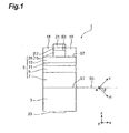
- Fig. 1 is a drawing for explaining a configuration of LD (laser diode) 1 according to an embodiment.
- LD 1 (a nitride-based semiconductor light emitting device) is provided with a GaN substrate 3, a GaN-based semiconductor region 5, an insulating film 19, a p-electrode 21, and an n-electrode 23.
- the n-electrode 23, GaN substrate 3, GaN-based semiconductor region 5, and p-electrode 21 are arranged in order along a predetermined z-axis direction.
- the GaN substrate 3 is provided between the n-electrode 23 and the GaN-based semiconductor region 5 (particularly, optical confinement layer 7), and is in contact with the n-electrode 23.
- the GaN substrate 3 has a primary surface S1.
- the primary surface S1 is opposite to the backside of the GaN substrate 3, and the n-electrode 23 is provided on the backside.
- the primary surface S1 extends along a reference plane S5 inclined at a predetermined inclination angle ⁇ with respect to a plane perpendicular to the c-axis direction of the GaN substrate 3.
- the inclination angle ⁇ is either in the range of more than 40° and less than 90° or in the range of not less than 150° and less than 180° (i.e., 40° ⁇ ⁇ ⁇ 90° or 150° ⁇ ⁇ ⁇ 180°), and more preferably is in the range of not less than 63° and less than 83° (i.e., 63° ⁇ ⁇ ⁇ 83°).
- the GaN-based semiconductor region 5 is provided between the GaN substrate 3 and the p-electrode 21, and is in contact with the primary surface S1 of the GaN substrate 3.
- the GaN-based semiconductor region 5 is comprised of hexagonal GaN-based semiconductors, and is provided on the primary surface S1,
- the GaN-based semiconductor region 5 is lattice-matched with the GaN substrate 3.
- the GaN-based semiconductor region 5 has an optical confinement layer 7, a light guide layer 9, a light emitting layer 11, a light guide layer 13, an optical confinement layer 15, and a contact layer 17.
- the optical confinement layer 7, light guide layer 9, light emitting layer 11, light guide layer 13, optical confinement layer 15, and contact layer 17 are arranged in order along the z-axis direction on the primary surface S1.
- the optical confinement layer 7 is provided between the GaN substrate 3 and the light guide layer 9, and is in contact with the primary surface S1 of the GaN substrate 3.
- the light guide layer 9 is provided between the optical confinement layer 7 and the light emitting layer 11, and is in contact with the optical confinement layer 7.
- the light emitting layer 11 is provided between the light guide layer 9 and the light guide layer 13, and is in contact with the light guide layer 9.
- the light emitting layer 11 has a multiple quantum well structure including a plurality of well layers and a plurality of barrier layers, and the light guide layer 9 is in contact with a barrier layer of the light emitting layer 11.
- a peak wavelength of the light emitting layer 11 is within a predetermined range of not less than 500 nm (preferably, in the range of not less than 500 nm and not more than 550 nm).
- the light guide layer 13 is provided between the light emitting layer 11 and the optical confinement layer 15, and is in contact with the light emitting layer 11 (particularly, a barrier layer).
- the optical confinement layer 15 is provided between the light guide layer 13 and the contact layer 17, and is in contact with the light guide layer 13.
- the contact layer 17 is provided between the optical confinement layer 15 and the p-electrode 21, and is in contact with the optical confinement layer 15.
- the optical confinement layer 15 is in contact with an interface S3 of the contact layer 17.
- the contact layer 17 is in contact with the p-electrode 21.
- the n-electrode 23 is in contact with the GaN substrate 3.
- the optical confinement layer 15 and the contact layer 17 constitute a stripe-shaped portion 25.
- the stripe-shaped portion 25 has a ridge shape that extends in the y-axis direction, and is provided on a part of a surface S7 of the light guide layer 13 (which is located on the opposite side to the interface to the light emitting layer 11).
- the insulating film 18, stripe-shaped portion 25, and insulating film 19 are arranged in order along the x-axis direction on the surface S7 of the light guide layer 13.
- the stripe-shaped portion 25 is provided between the insulating film 18 and the insulating film 19, and is in contact with the insulating film 18 and the insulating film 19.
- the insulating film 18 and the insulating film 19 are in contact with the surface S7 of the light guide layer 13.
- the optical confinement layer 7 is comprised of InAlGaN (a composition ratio of In of which is 3% and a composition ratio of Al of which is 14%) or AlGaN (a composition ratio of Al of which is 7%) and has the thickness of about 1200 nm.
- the light guide layer 9 and the light guide layer 13 both are comprised of InGaN (a composition ratio of In of which is 3%) and have the thickness of about 100 nm.
- the well layers in the light emitting layer 11 all are comprised of InGaN (a composition ratio of In of which is 30%), and have the thickness of about 3 nm.
- the barrier layers in the light emitting layer 11 all are comprised of InGaN (a composition ratio of In of which is from 0 to 3%) and have the thickness of about 10 nm.
- a wavelength band of the light emitting layer 11 is a 520 nm band.
- the optical confinement layer 15 is comprised of p-type doped AlGaN (a composition ratio of Al of which is 7%) or p-type doped InAlGaN (a composition ratio of In of which is 3% and a composition ratio of Al of which is 14%), and has the thickness of about 400 nm.
- the contact layer 17 is comprised of p-type doped InGaN or p-type doped InAlGaN, and has the thickness of about 10 to 50 nm. When the contact layer 17 is comprised of p-type doped InGaN, the composition ratio of In of the contact layer 17 is in the range of not less than 1% and not more than 20%.
- the composition ratio of In of the contact layer 17 is larger than a value obtained by multiplying the composition ratio of Al of the contact layer 17 by 0.22.
- the bandgap energy of the optical confinement layer 15 is larger than that of the contact layer 17.
- the insulating film 19 is comprised of SiO 2 .
- the p-electrode 21 is comprised of any one ofNi/Au, Pt/Pd, Pd/Au, Al/Ti/Al, Ni/Pt/Au, and Pd/Pt/Au.
- the n-electrode 23 is comprised of Ti/Al.
- the width of the GaN-based semiconductor region 5 in an in-plane direction along the reference plane S5 is about 400 ⁇ m, and the height thereof in the direction perpendicular to the reference plane S5 is about 100 ⁇ m.
- the stripe-shaped portion 25 has the width of about 2 ⁇ m in the in-plane direction along the reference plane S5 of the GaN-based semiconductor region 5 and the height of about 1 ⁇ m in the direction perpendicular to the reference plane S5.
- a GaN-based semiconductor region corresponding to the GaN-based semiconductor region 5 is formed on a surface of a GaN substrate corresponding to the GaN substrate 3.
- a portion corresponding to the stripe-shaped portion 25 is formed by dry etching.
- SiO 2 insulating film corresponding to the insulating film 18 and the insulating film 19 is deposited by sputtering on a surface formed by the dry etching, and thereafter the p-electrode 21 is formed, followed by division into a plurality of LDs 1,
- the GaN substrate 3 and the GaN-based semiconductor region 5 are lattice-matched with each other and therefore compressive stress is in the in-plane direction along the reference plane S5 in the contact layer 17 comprised of p-type doped InGaN or p-type doped InAlGaN; consequently, a negative piezoelectric field is in the contact layer 17.
- This negative piezoelectric field varies the energy band in the contact layer 17 so as to reduce the Schottky barrier at the interface. Therefore, the operating voltage of LD 1 is reduced.
- an actually measured value of the operating voltage of another LD using a contact layer 17a comprised of p-type doped GaN instead of the contact layer 17 of LD 1 was 10 (Volts), whereas an actually measured value of the operating voltage of LD 1 was 6 (Volts).
- Part (a) of Fig. 2 shows the bandgap diagram of the optical confinement layer 15 and the contact layer 17.
- Part (b) of Fig. 2 shows the bandgap diagram of the optical confinement layer 15 and the contact layer 17a of the other LD in which the contact layer 17a of p-type doped GaN is used instead of the contact layer 17 of LD 1 according to the present embodiment.
- reference symbol F represents the Fermi level
- arrow symbol H represents a direction of Hall current.
- the bandgap of the contact layer 17 of LD 1 is varied such that the Schottky barrier SB1 of the contact layer 17 of LD1 becomes smaller than the Schottky barrier SB2 of the contact layer 17a of the other LD.
- the Schottky barrier of energy band in the contact layer 17 is reduced when the composition ratio of In of the contact layer 17 is not less than 1%, and the compressive stress is released by lattice relaxation in the contact layer 17 with the thickness of 10-50 nm when the composition ratio of In of the contact layer 17 is more than 20%, Therefore, the composition ratio of In of the contact layer 17 is defined in the range of not less than 1% and not more than 20%.
- the composition ratio of In of the contact layer 17 is set to a value larger than a value obtained by multiplying the composition ratio of Al of the contact layer 17 by 0.22.
- the inclination angle ⁇ is in the range of not less than 63° and less than 83°, the negative piezoelectric field becomes maximum and therefore the drive voltage of LD 1 according to the present embodiment can be fully reduced.
- a peak wavelength of the aforementioned other LD is not less than 500 nm, a voltage drop in the light emitting layer 11 becomes prominent to increase the overall drive voltage of LD 1.
- the wavelength band of LD 1 according to the present embodiment is the 520 nm band, while achieving the reduction in drive voltage when compared with the foregoing other LD.
Landscapes
- Chemical & Material Sciences (AREA)
- Engineering & Computer Science (AREA)
- Nanotechnology (AREA)
- Physics & Mathematics (AREA)
- Life Sciences & Earth Sciences (AREA)
- Biophysics (AREA)
- Optics & Photonics (AREA)
- Crystallography & Structural Chemistry (AREA)
- Semiconductor Lasers (AREA)
- Led Devices (AREA)
- Electrodes Of Semiconductors (AREA)
Abstract
Description
- The present invention relates to a nitride-based semiconductor light emitting device.
-
Patent Document 1 discloses a structure of high-efficiency GaN (gallium nitride)-based optical semiconductor device. The light emitting device being the optical semiconductor device ofPatent Document 1 is provided with a plurality of GaN-based semiconductor layers including strained quantum well layers. This light emitting device is formed by successively depositing an n-type GaN contact layer, an n-type AlGaN cladding layer, multiple strained quantum well layers, a p-type AlGaN cladding layer, and a p-type GaN contact layer on a substrate of sapphire, SiC, GaN, or the like. Furthermore, an n-electrode and a p-electrode are formed on the n-type GaN contact layer and on the p-type GaN contact layer, respectively, as electrodes for the respective layers, The multiple strained quantum well layers used are GaInN/GaN multiple strained quantum well layers or GaInN/GaInN multiple strained quantum well layers. The plane orientation of the growth face of the multiple strained quantum well layers is different from the orientation in which the piezoelectric field is maximum.Patent Document 1; Japanese Patent Application Laid-open No.11-112029 - The above-described conventional optical semiconductor device is provided with the p-type GaN contact layer and the p-electrode, and the p-electrode is in contact with the p-type GaN contact layer. When the optical semiconductor device is constructed in this structure, p-type GaN has a relatively large work function and thus a Schottky barrier can be formed at an interface between the p-type GaN contact layer and the p-electrode. It is therefore an object of the present invention to provide a nitride-based semiconductor light emitting device capable of preventing the Schottky barrier from being formed at the interface between the contact layer and the electrode.
- One aspect of the present invention relates to a nitride-based semiconductor light emitting device. The nitride-based semiconductor light emitting device comprises: a GaN substrate; a hexagonal GaN-based semiconductor region provided on a primary surface of the GaN substrate and comprising a light emitting layer; and an electrode provided on the GaN-based semiconductor region and comprised of metal, the GaN-based semiconductor region comprising a contact layer, the contact layer being strained, the contact layer being in contact with the electrode, the primary surface extending along a reference plane, the reference plane being inclined at a predetermined inclination angle with respect to a plane perpendicular to a c-axis direction of the GaN substrate, the inclination angle being either in the range of more than 40° and less than 90° or in the range of not less than 150° and less than 180°, the GaN-based semiconductor region being lattice-matched with the GaN substrate, the contact layer being comprised of p-type doped InGaN or p-type doped InAlGaN, the contact layer of the p-type doped InGaN having a composition ratio of In in the range of not less than 1% and not more than 20%, and the contact layer of the p-type doped InAlGaN having a composition ratio of In larger than a value obtained by multiplying a composition ratio of A1 of the contact layer by 0.22.
- In the aspect of the present invention, when the angle between the primary surface of the GaN substrate and the plane perpendicular to the c-axis direction of the GaN substrate is either in the range of more than 40° and less than 90° or in the range of not less than 150° and less than 180°, the GaN substrate is lattice-matched with the Gay-basted semiconductor region and compressive stress is thus in an in-plane direction along the reference plane in the contact layer comprised of p-type doped InGaN or p-type doped InAlGaN; consequently, a negative piezoelectric field is in the contact layer. This negative piezoelectric field varies the energy band in the contact layer so as to reduce the Schottky barrier at the interface. When the contact layer is comprised of p-type doped InGaN, the compressive stress remains without being released by lattice relaxation in the contact layer, for example, with the thickness of 10-50 nm, as long as the composition ratio of In of the contact layer is in the range of not less than 1% and not more than 20%; therefore, the Schottky barrier of energy band in the contact layer is reduced, When the contact layer is comprised of p-type doped InAlCaN, the contact layer has the compressive stress on the GaN substrate if the composition ratio of In of the contact layer is larger than a value obtained by multiplying the composition ratio of Al of the contact layer by 0.22.
- In the aforementioned aspect of the present invention, the inclination angle is preferably in the range of not less than 63° and less than 83°. When the inclination angle is in the range of not less than 63° and less than 83°, the negative piezoelectric field becomes maximum and the drive voltage is fully reduced.
- In the aforementioned aspect of the present invention, a peak wavelength of the light emitting layer is within a predetermined range of not less than 500 nm. Therefore, the drive voltage is reduced even in the case of the peak wavelength of not less than 500 nm where a voltage drop in the light emitting layer becomes prominent and the drive voltage of the entire device becomes high.
- The aforementioned aspect of the present invention provides the nitride-based semiconductor light emitting device capable of preventing the Schottky barrier from being formed at the interface between the contact layer and the electrode.
-
-
Fig. 1 is a drawing for explaining a configuration of LD according to an embodiment. -
Fig. 2 is a drawing for explaining the effect of LD according to the embodiment. - Embodiments according to the present invention will be described below in detail with reference to the drawings. In the description of the drawings, the same elements will be denoted by the same reference symbols as much as possible, without redundant description.
Fig. 1 is a drawing for explaining a configuration of LD (laser diode) 1 according to an embodiment. LD 1 (a nitride-based semiconductor light emitting device) is provided with aGaN substrate 3, a GaN-basedsemiconductor region 5, aninsulating film 19, a p-electrode 21, and an n-electrode 23. The n-electrode 23,GaN substrate 3, GaN-basedsemiconductor region 5, and p-electrode 21 are arranged in order along a predetermined z-axis direction. - The
GaN substrate 3 is provided between the n-electrode 23 and the GaN-based semiconductor region 5 (particularly, optical confinement layer 7), and is in contact with the n-electrode 23. The GaNsubstrate 3 has a primary surface S1. The primary surface S1 is opposite to the backside of theGaN substrate 3, and the n-electrode 23 is provided on the backside. The primary surface S1 extends along a reference plane S5 inclined at a predetermined inclination angle θ with respect to a plane perpendicular to the c-axis direction of theGaN substrate 3. The inclination angle θ is either in the range of more than 40° and less than 90° or in the range of not less than 150° and less than 180° (i.e., 40° < θ < 90° or 150° ≤ θ < 180°), and more preferably is in the range of not less than 63° and less than 83° (i.e., 63° ≤ θ < 83°). - The GaN-based
semiconductor region 5 is provided between theGaN substrate 3 and the p-electrode 21, and is in contact with the primary surface S1 of theGaN substrate 3. The GaN-basedsemiconductor region 5 is comprised of hexagonal GaN-based semiconductors, and is provided on the primary surface S1, The GaN-basedsemiconductor region 5 is lattice-matched with theGaN substrate 3. The GaN-basedsemiconductor region 5 has anoptical confinement layer 7, alight guide layer 9, a light emitting layer 11, alight guide layer 13, anoptical confinement layer 15, and acontact layer 17. Theoptical confinement layer 7,light guide layer 9, light emitting layer 11,light guide layer 13,optical confinement layer 15, andcontact layer 17 are arranged in order along the z-axis direction on the primary surface S1. - The
optical confinement layer 7 is provided between theGaN substrate 3 and thelight guide layer 9, and is in contact with the primary surface S1 of theGaN substrate 3. Thelight guide layer 9 is provided between theoptical confinement layer 7 and the light emitting layer 11, and is in contact with theoptical confinement layer 7. The light emitting layer 11 is provided between thelight guide layer 9 and thelight guide layer 13, and is in contact with thelight guide layer 9. The light emitting layer 11 has a multiple quantum well structure including a plurality of well layers and a plurality of barrier layers, and thelight guide layer 9 is in contact with a barrier layer of the light emitting layer 11. A peak wavelength of the light emitting layer 11 is within a predetermined range of not less than 500 nm (preferably, in the range of not less than 500 nm and not more than 550 nm). Thelight guide layer 13 is provided between the light emitting layer 11 and theoptical confinement layer 15, and is in contact with the light emitting layer 11 (particularly, a barrier layer). - The
optical confinement layer 15 is provided between thelight guide layer 13 and thecontact layer 17, and is in contact with thelight guide layer 13. Thecontact layer 17 is provided between theoptical confinement layer 15 and the p-electrode 21, and is in contact with theoptical confinement layer 15. Theoptical confinement layer 15 is in contact with an interface S3 of thecontact layer 17. Thecontact layer 17 is in contact with the p-electrode 21. The n-electrode 23 is in contact with theGaN substrate 3. - The
optical confinement layer 15 and thecontact layer 17 constitute a stripe-shaped portion 25. The stripe-shaped portion 25 has a ridge shape that extends in the y-axis direction, and is provided on a part of a surface S7 of the light guide layer 13 (which is located on the opposite side to the interface to the light emitting layer 11). Theinsulating film 18, stripe-shaped portion 25, andinsulating film 19 are arranged in order along the x-axis direction on the surface S7 of thelight guide layer 13. The stripe-shaped portion 25 is provided between theinsulating film 18 and theinsulating film 19, and is in contact with theinsulating film 18 and theinsulating film 19. Theinsulating film 18 and theinsulating film 19 are in contact with the surface S7 of thelight guide layer 13. - The below describes an example of
LD 1. A 75°-off plane ((20-21) plane) tilting toward the m-axis direction is used as theprimary surface S 1 of theCaN substrate 3. Theoptical confinement layer 7 is comprised of InAlGaN (a composition ratio of In of which is 3% and a composition ratio of Al of which is 14%) or AlGaN (a composition ratio of Al of which is 7%) and has the thickness of about 1200 nm. Thelight guide layer 9 and thelight guide layer 13 both are comprised of InGaN (a composition ratio of In of which is 3%) and have the thickness of about 100 nm. The well layers in the light emitting layer 11 all are comprised of InGaN (a composition ratio of In of which is 30%), and have the thickness of about 3 nm. The barrier layers in the light emitting layer 11 all are comprised of InGaN (a composition ratio of In of which is from 0 to 3%) and have the thickness of about 10 nm. A wavelength band of the light emitting layer 11 is a 520 nm band. - The
optical confinement layer 15 is comprised of p-type doped AlGaN (a composition ratio of Al of which is 7%) or p-type doped InAlGaN (a composition ratio of In of which is 3% and a composition ratio of Al of which is 14%), and has the thickness of about 400 nm. Thecontact layer 17 is comprised of p-type doped InGaN or p-type doped InAlGaN, and has the thickness of about 10 to 50 nm. When thecontact layer 17 is comprised of p-type doped InGaN, the composition ratio of In of thecontact layer 17 is in the range of not less than 1% and not more than 20%. When thecontact layer 17 is comprised of p-type doped InAlGaN, the composition ratio of In of thecontact layer 17 is larger than a value obtained by multiplying the composition ratio of Al of thecontact layer 17 by 0.22. The bandgap energy of theoptical confinement layer 15 is larger than that of thecontact layer 17. - The insulating
film 19 is comprised of SiO2. The p-electrode 21 is comprised of any one ofNi/Au, Pt/Pd, Pd/Au, Al/Ti/Al, Ni/Pt/Au, and Pd/Pt/Au. The n-electrode 23 is comprised of Ti/Al. - The width of the GaN-based
semiconductor region 5 in an in-plane direction along the reference plane S5 is about 400 µm, and the height thereof in the direction perpendicular to the reference plane S5 is about 100 µm. The stripe-shaped portion 25 has the width of about 2 µm in the in-plane direction along the reference plane S5 of the GaN-basedsemiconductor region 5 and the height of about 1 µm in the direction perpendicular to the reference plane S5. - The below schematically describes a method of fabricating
LD 1 according to the embodiment. First, a GaN-based semiconductor region corresponding to the GaN-basedsemiconductor region 5 is formed on a surface of a GaN substrate corresponding to theGaN substrate 3. Next, a portion corresponding to the stripe-shaped portion 25 is formed by dry etching. Then SiO2 insulating film corresponding to the insulatingfilm 18 and the insulatingfilm 19 is deposited by sputtering on a surface formed by the dry etching, and thereafter the p-electrode 21 is formed, followed by division into a plurality ofLDs 1, - With
LD 1 according to the present embodiment described above, when the angle (inclination angle θ) between the primary surface S1 and the plane perpendicular to the c-axis direction of theGaN substrate 3 is either in the range of more than 40° and less than 90° or in the range of not less than 150° and less than 180°, theGaN substrate 3 and the GaN-basedsemiconductor region 5 are lattice-matched with each other and therefore compressive stress is in the in-plane direction along the reference plane S5 in thecontact layer 17 comprised of p-type doped InGaN or p-type doped InAlGaN; consequently, a negative piezoelectric field is in thecontact layer 17. This negative piezoelectric field varies the energy band in thecontact layer 17 so as to reduce the Schottky barrier at the interface. Therefore, the operating voltage ofLD 1 is reduced. In fact, an actually measured value of the operating voltage of another LD using acontact layer 17a comprised of p-type doped GaN instead of thecontact layer 17 ofLD 1 was 10 (Volts), whereas an actually measured value of the operating voltage ofLD 1 was 6 (Volts). - Part (a) of
Fig. 2 shows the bandgap diagram of theoptical confinement layer 15 and thecontact layer 17. Part (b) ofFig. 2 shows the bandgap diagram of theoptical confinement layer 15 and thecontact layer 17a of the other LD in which thecontact layer 17a of p-type doped GaN is used instead of thecontact layer 17 ofLD 1 according to the present embodiment. In the drawing, reference symbol F represents the Fermi level and arrow symbol H represents a direction of Hall current. As shown in Part (a) ofFig. 2 and Part (b) ofFig. 2 , the bandgap of thecontact layer 17 ofLD 1 is varied such that the Schottky barrier SB1 of thecontact layer 17 of LD1 becomes smaller than the Schottky barrier SB2 of thecontact layer 17a of the other LD. - In the
contact layer 17 of p-type doped InGaN, the Schottky barrier of energy band in thecontact layer 17 is reduced when the composition ratio of In of thecontact layer 17 is not less than 1%, and the compressive stress is released by lattice relaxation in thecontact layer 17 with the thickness of 10-50 nm when the composition ratio of In of thecontact layer 17 is more than 20%, Therefore, the composition ratio of In of thecontact layer 17 is defined in the range of not less than 1% and not more than 20%. In thecontact layer 17 of p-type doped InAlGaN, in order to provide thecontact layer 17 with compressive stress on theGaN substrate 3, the composition ratio of In of thecontact layer 17 is set to a value larger than a value obtained by multiplying the composition ratio of Al of thecontact layer 17 by 0.22. When the inclination angle θ is in the range of not less than 63° and less than 83°, the negative piezoelectric field becomes maximum and therefore the drive voltage ofLD 1 according to the present embodiment can be fully reduced. If a peak wavelength of the aforementioned other LD is not less than 500 nm, a voltage drop in the light emitting layer 11 becomes prominent to increase the overall drive voltage ofLD 1. In contrast to it, the wavelength band ofLD 1 according to the present embodiment is the 520 nm band, while achieving the reduction in drive voltage when compared with the foregoing other LD. - The principle of the present invention was illustrated and explained in the preferred embodiments, but it is recognized by those skilled in the art that the present invention can be modified in arrangement and detail without departing from the principle. The present invention is by no means limited to the specific configurations disclosed in the embodiments. Therefore, the applicant claims all modifications and changes falling within the scope of claims and coming from the scope of spirit thereof.
Claims (3)
- A nitride-based semiconductor light emitting device comprising:a GaN substrate;a hexagonal GaN-based semiconductor region provided on a primary surface of the GaN substrate and comprising a light emitting layer; andan electrode provided on the GaN-based semiconductor region and comprised of metal,the GaN-based semiconductor region comprising a contact layer,the contact layer being strained,the contact layer being in contact with the electrode,the primary surface extending along a reference plane,the reference plane being inclined at a predetermined inclination angle with respect to a plane perpendicular to a c-axis direction of the GaN substrate,the inclination angle being either in the range of more than 40° and less than 90° or in the range of not less than 150° to less than 180°,the GaN-based semiconductor region being lattice-matched with the GaN substrate,the contact layer being comprised of p-type doped InGaN or p-type doped InAlGaN,the contact layer of the p-type doped InGaN having a composition ratio of In in the range of not less than 1% and not more than 20%, andthe contact layer of the p-type doped InAlGaN having a composition ratio of In larger than a value obtained by multiplying a composition ratio of Al of the contact layer by 0.22.
- The nitride-based semiconductor light emitting device according to claim 1, wherein the inclination angle is in the range of not less than 63° and less than 83°.
- The nitride-based semiconductor light emitting device according to claim 1 or claim 2, wherein a peak wavelength of the light emitting layer is within a predetermined range of not less than 500 nm.
Applications Claiming Priority (1)
| Application Number | Priority Date | Filing Date | Title |
|---|---|---|---|
| JP2009166924A JP4905514B2 (en) | 2009-07-15 | 2009-07-15 | Nitride semiconductor light emitting device |
Publications (2)
| Publication Number | Publication Date |
|---|---|
| EP2276079A2 true EP2276079A2 (en) | 2011-01-19 |
| EP2276079A3 EP2276079A3 (en) | 2011-07-06 |
Family
ID=43012777
Family Applications (1)
| Application Number | Title | Priority Date | Filing Date |
|---|---|---|---|
| EP10169585A Withdrawn EP2276079A3 (en) | 2009-07-15 | 2010-07-15 | Nitride-based semiconductor light emitting device |
Country Status (6)
| Country | Link |
|---|---|
| US (1) | US8174035B2 (en) |
| EP (1) | EP2276079A3 (en) |
| JP (1) | JP4905514B2 (en) |
| KR (1) | KR101216342B1 (en) |
| CN (1) | CN101958386A (en) |
| TW (1) | TW201115787A (en) |
Cited By (1)
| Publication number | Priority date | Publication date | Assignee | Title |
|---|---|---|---|---|
| CN103493316A (en) * | 2011-04-22 | 2014-01-01 | 住友电气工业株式会社 | Nitride semiconductor laser and epitaxial substrate |
Families Citing this family (1)
| Publication number | Priority date | Publication date | Assignee | Title |
|---|---|---|---|---|
| DE102017119931A1 (en) * | 2017-08-30 | 2019-02-28 | Osram Opto Semiconductors Gmbh | Optoelectronic semiconductor component |
Citations (1)
| Publication number | Priority date | Publication date | Assignee | Title |
|---|---|---|---|---|
| JPH11112029A (en) | 1997-09-30 | 1999-04-23 | Hewlett Packard Co <Hp> | Optical semiconductor device and method of manufacturing the same |
Family Cites Families (16)
| Publication number | Priority date | Publication date | Assignee | Title |
|---|---|---|---|---|
| JP2001339121A (en) * | 2000-05-29 | 2001-12-07 | Sharp Corp | Nitride semiconductor light emitting device and optical device including the same |
| JP4416297B2 (en) * | 2000-09-08 | 2010-02-17 | シャープ株式会社 | Nitride semiconductor light emitting element, and light emitting device and optical pickup device using the same |
| US6734530B2 (en) | 2001-06-06 | 2004-05-11 | Matsushita Electric Industries Co., Ltd. | GaN-based compound semiconductor EPI-wafer and semiconductor element using the same |
| TW502438B (en) | 2001-07-23 | 2002-09-11 | Uni Light Technology Inc | Semiconductor device with ohmic contact and method for producing the same |
| TWI262606B (en) | 2001-08-30 | 2006-09-21 | Osram Opto Semiconductors Gmbh | Radiation-emitting semiconductor-element and its production method |
| ATE418806T1 (en) * | 2004-04-02 | 2009-01-15 | Nichia Corp | NITRIDE SEMICONDUCTOR LASER DEVICE |
| JP4301136B2 (en) * | 2004-10-18 | 2009-07-22 | サンケン電気株式会社 | Semiconductor light emitting device and manufacturing method thereof |
| US7751455B2 (en) | 2004-12-14 | 2010-07-06 | Palo Alto Research Center Incorporated | Blue and green laser diodes with gallium nitride or indium gallium nitride cladding laser structure |
| EP2315253A1 (en) * | 2005-03-10 | 2011-04-27 | The Regents of the University of California | Technique for the growth of planar semi-polar gallium nitride |
| JP2008258503A (en) | 2007-04-06 | 2008-10-23 | Sumitomo Electric Ind Ltd | Nitride-based semiconductor light-emitting device and method for manufacturing nitride-based semiconductor light-emitting device |
| JP2009016467A (en) * | 2007-07-03 | 2009-01-22 | Sony Corp | Gallium nitride semiconductor device, optical device using the same, and image display device using the same |
| JP2009021361A (en) | 2007-07-11 | 2009-01-29 | Sumitomo Electric Ind Ltd | Nitride-based semiconductor light-emitting device and method for manufacturing nitride-based semiconductor light-emitting device |
| JP2009081336A (en) * | 2007-09-27 | 2009-04-16 | Sanyo Electric Co Ltd | Nitride-based semiconductor laser element and its manufacturing method |
| JP2009081374A (en) * | 2007-09-27 | 2009-04-16 | Rohm Co Ltd | Semiconductor light emitting device |
| JP2010016092A (en) * | 2008-07-02 | 2010-01-21 | Sharp Corp | Nitride system semiconductor light-emitting element |
| JP2010118647A (en) * | 2008-10-17 | 2010-05-27 | Sumitomo Electric Ind Ltd | Nitride-based semiconductor light emitting element, method of manufacturing nitride-based semiconductor light emitting element, and light emitting device |
-
2009
- 2009-07-15 JP JP2009166924A patent/JP4905514B2/en not_active Expired - Fee Related
-
2010
- 2010-07-13 KR KR1020100067490A patent/KR101216342B1/en not_active Expired - Fee Related
- 2010-07-14 US US12/836,090 patent/US8174035B2/en not_active Expired - Fee Related
- 2010-07-15 EP EP10169585A patent/EP2276079A3/en not_active Withdrawn
- 2010-07-15 TW TW099123322A patent/TW201115787A/en unknown
- 2010-07-15 CN CN2010102313676A patent/CN101958386A/en active Pending
Patent Citations (1)
| Publication number | Priority date | Publication date | Assignee | Title |
|---|---|---|---|---|
| JPH11112029A (en) | 1997-09-30 | 1999-04-23 | Hewlett Packard Co <Hp> | Optical semiconductor device and method of manufacturing the same |
Cited By (1)
| Publication number | Priority date | Publication date | Assignee | Title |
|---|---|---|---|---|
| CN103493316A (en) * | 2011-04-22 | 2014-01-01 | 住友电气工业株式会社 | Nitride semiconductor laser and epitaxial substrate |
Also Published As
| Publication number | Publication date |
|---|---|
| JP2011023524A (en) | 2011-02-03 |
| KR101216342B1 (en) | 2012-12-27 |
| KR20110007046A (en) | 2011-01-21 |
| TW201115787A (en) | 2011-05-01 |
| CN101958386A (en) | 2011-01-26 |
| US8174035B2 (en) | 2012-05-08 |
| EP2276079A3 (en) | 2011-07-06 |
| US20110012126A1 (en) | 2011-01-20 |
| JP4905514B2 (en) | 2012-03-28 |
Similar Documents
| Publication | Publication Date | Title |
|---|---|---|
| EP2747220B1 (en) | Nitride semiconductor ultraviolet light emitting element | |
| JP4328366B2 (en) | Semiconductor element | |
| KR100906760B1 (en) | Nitride semiconductor devices | |
| EP2736130B1 (en) | Nitride semiconductor laser element | |
| EP1914813A2 (en) | Semiconductor optoelectronic device | |
| EP1959530A1 (en) | Gallium nitride semiconductor light emitting element | |
| JP7545084B2 (en) | Semiconductor laser element | |
| KR20130141709A (en) | Group iii nitride semiconductor element and method for manufacturing group iii nitride semiconductor element | |
| JP3754226B2 (en) | Semiconductor light emitting device | |
| US10686298B2 (en) | Method of manufacturing semiconductor laser device | |
| US8174035B2 (en) | Nitride-based semiconductor light emitting device | |
| CN105742442B (en) | The manufacturing method of nitride-based semiconductor ultraviolet ray emitting element | |
| JP2007214221A (en) | Nitride semiconductor laser device | |
| JP7563696B2 (en) | Method for manufacturing ultraviolet laser diode and ultraviolet laser diode | |
| WO2007032355A1 (en) | Semiconductor light-emitting device | |
| WO2024225306A1 (en) | Light-emitting semiconductor element and method for manufacturing same | |
| JP2012094896A (en) | Nitride-based semiconductor light-emitting element | |
| KR20080091603A (en) | Laser diode and manufacturing method thereof | |
| JP2006190803A (en) | Semiconductor light emitting device | |
| JP2015216303A (en) | Semiconductor laser element | |
| JP2007081181A (en) | Semiconductor light emitting device |
Legal Events
| Date | Code | Title | Description |
|---|---|---|---|
| PUAI | Public reference made under article 153(3) epc to a published international application that has entered the european phase |
Free format text: ORIGINAL CODE: 0009012 |
|
| AK | Designated contracting states |
Kind code of ref document: A2 Designated state(s): AL AT BE BG CH CY CZ DE DK EE ES FI FR GB GR HR HU IE IS IT LI LT LU LV MC MK MT NL NO PL PT RO SE SI SK SM TR |
|
| AX | Request for extension of the european patent |
Extension state: BA ME RS |
|
| REG | Reference to a national code |
Ref country code: DE Ref legal event code: R079 Free format text: PREVIOUS MAIN CLASS: H01L0033160000 Ipc: H01S0005042000 |
|
| PUAL | Search report despatched |
Free format text: ORIGINAL CODE: 0009013 |
|
| AK | Designated contracting states |
Kind code of ref document: A3 Designated state(s): AL AT BE BG CH CY CZ DE DK EE ES FI FR GB GR HR HU IE IS IT LI LT LU LV MC MK MT NL NO PL PT RO SE SI SK SM TR |
|
| AX | Request for extension of the european patent |
Extension state: BA ME RS |
|
| RIC1 | Information provided on ipc code assigned before grant |
Ipc: H01L 33/14 20100101ALN20110601BHEP Ipc: H01L 33/02 20100101ALN20110601BHEP Ipc: H01L 33/32 20100101ALI20110601BHEP Ipc: H01L 33/16 20100101ALI20110601BHEP Ipc: H01S 5/343 20060101ALI20110601BHEP Ipc: H01S 5/042 20060101AFI20110601BHEP |
|
| 17P | Request for examination filed |
Effective date: 20120109 |
|
| STAA | Information on the status of an ep patent application or granted ep patent |
Free format text: STATUS: THE APPLICATION HAS BEEN WITHDRAWN |
|
| 18W | Application withdrawn |
Effective date: 20150312 |