EP2276082B1 - Magnetempfindlicher draht, magnetimpedanzelement und magnetimpedanzsensor - Google Patents
Magnetempfindlicher draht, magnetimpedanzelement und magnetimpedanzsensor Download PDFInfo
- Publication number
- EP2276082B1 EP2276082B1 EP09724160.8A EP09724160A EP2276082B1 EP 2276082 B1 EP2276082 B1 EP 2276082B1 EP 09724160 A EP09724160 A EP 09724160A EP 2276082 B1 EP2276082 B1 EP 2276082B1
- Authority
- EP
- European Patent Office
- Prior art keywords
- magneto
- wire
- sensitive wire
- sensor
- sensitive
- Prior art date
- Legal status (The legal status is an assumption and is not a legal conclusion. Google has not performed a legal analysis and makes no representation as to the accuracy of the status listed.)
- Active
Links
Images

Classifications
-
- G—PHYSICS
- G01—MEASURING; TESTING
- G01R—MEASURING ELECTRIC VARIABLES; MEASURING MAGNETIC VARIABLES
- G01R33/00—Arrangements or instruments for measuring magnetic variables
- G01R33/02—Measuring direction or magnitude of magnetic fields or magnetic flux
- G01R33/06—Measuring direction or magnitude of magnetic fields or magnetic flux using galvano-magnetic devices
- G01R33/09—Magnetoresistive devices
- G01R33/093—Magnetoresistive devices using multilayer structures, e.g. giant magnetoresistance sensors
-
- B—PERFORMING OPERATIONS; TRANSPORTING
- B82—NANOTECHNOLOGY
- B82Y—SPECIFIC USES OR APPLICATIONS OF NANOSTRUCTURES; MEASUREMENT OR ANALYSIS OF NANOSTRUCTURES; MANUFACTURE OR TREATMENT OF NANOSTRUCTURES
- B82Y25/00—Nanomagnetism, e.g. magnetoimpedance, anisotropic magnetoresistance, giant magnetoresistance or tunneling magnetoresistance
-
- G—PHYSICS
- G01—MEASURING; TESTING
- G01R—MEASURING ELECTRIC VARIABLES; MEASURING MAGNETIC VARIABLES
- G01R33/00—Arrangements or instruments for measuring magnetic variables
- G01R33/02—Measuring direction or magnitude of magnetic fields or magnetic flux
- G01R33/06—Measuring direction or magnitude of magnetic fields or magnetic flux using galvano-magnetic devices
- G01R33/063—Magneto-impedance sensors; Nanocristallin sensors
-
- G—PHYSICS
- G01—MEASURING; TESTING
- G01R—MEASURING ELECTRIC VARIABLES; MEASURING MAGNETIC VARIABLES
- G01R33/00—Arrangements or instruments for measuring magnetic variables
- G01R33/12—Measuring magnetic properties of articles or specimens of solids or fluids
- G01R33/1284—Spin resolved measurements; Influencing spins during measurements, e.g. in spintronics devices
-
- H—ELECTRICITY
- H10—SEMICONDUCTOR DEVICES; ELECTRIC SOLID-STATE DEVICES NOT OTHERWISE PROVIDED FOR
- H10N—ELECTRIC SOLID-STATE DEVICES NOT OTHERWISE PROVIDED FOR
- H10N50/00—Galvanomagnetic devices
- H10N50/10—Magnetoresistive devices
-
- H—ELECTRICITY
- H10—SEMICONDUCTOR DEVICES; ELECTRIC SOLID-STATE DEVICES NOT OTHERWISE PROVIDED FOR
- H10N—ELECTRIC SOLID-STATE DEVICES NOT OTHERWISE PROVIDED FOR
- H10N50/00—Galvanomagnetic devices
- H10N50/80—Constructional details
- H10N50/85—Materials of the active region
-
- Y—GENERAL TAGGING OF NEW TECHNOLOGICAL DEVELOPMENTS; GENERAL TAGGING OF CROSS-SECTIONAL TECHNOLOGIES SPANNING OVER SEVERAL SECTIONS OF THE IPC; TECHNICAL SUBJECTS COVERED BY FORMER USPC CROSS-REFERENCE ART COLLECTIONS [XRACs] AND DIGESTS
- Y10—TECHNICAL SUBJECTS COVERED BY FORMER USPC
- Y10T—TECHNICAL SUBJECTS COVERED BY FORMER US CLASSIFICATION
- Y10T428/00—Stock material or miscellaneous articles
- Y10T428/12—All metal or with adjacent metals
- Y10T428/12431—Foil or filament smaller than 6 mils
- Y10T428/12438—Composite
-
- Y—GENERAL TAGGING OF NEW TECHNOLOGICAL DEVELOPMENTS; GENERAL TAGGING OF CROSS-SECTIONAL TECHNOLOGIES SPANNING OVER SEVERAL SECTIONS OF THE IPC; TECHNICAL SUBJECTS COVERED BY FORMER USPC CROSS-REFERENCE ART COLLECTIONS [XRACs] AND DIGESTS
- Y10—TECHNICAL SUBJECTS COVERED BY FORMER USPC
- Y10T—TECHNICAL SUBJECTS COVERED BY FORMER US CLASSIFICATION
- Y10T428/00—Stock material or miscellaneous articles
- Y10T428/12—All metal or with adjacent metals
- Y10T428/12493—Composite; i.e., plural, adjacent, spatially distinct metal components [e.g., layers, joint, etc.]
-
- Y—GENERAL TAGGING OF NEW TECHNOLOGICAL DEVELOPMENTS; GENERAL TAGGING OF CROSS-SECTIONAL TECHNOLOGIES SPANNING OVER SEVERAL SECTIONS OF THE IPC; TECHNICAL SUBJECTS COVERED BY FORMER USPC CROSS-REFERENCE ART COLLECTIONS [XRACs] AND DIGESTS
- Y10—TECHNICAL SUBJECTS COVERED BY FORMER USPC
- Y10T—TECHNICAL SUBJECTS COVERED BY FORMER US CLASSIFICATION
- Y10T428/00—Stock material or miscellaneous articles
- Y10T428/12—All metal or with adjacent metals
- Y10T428/12493—Composite; i.e., plural, adjacent, spatially distinct metal components [e.g., layers, joint, etc.]
- Y10T428/12771—Transition metal-base component
- Y10T428/12861—Group VIII or IB metal-base component
Definitions
- the present invention relates to a method of manufacturing a magneto-sensitive-wire, a magneto-sensitive wire manufactured by this method and having good hysteresis characteristics, and a magneto-impedance element (hereinafter referred to as an "MI element”) or a magneto-impedance sensor (hereinafter referred to as an "MI sensor”) employing the magneto-sensitive wire.
- a magneto-impedance element hereinafter referred to as an "MI element”
- MI sensor magneto-impedance sensor
- the pick-up coil wound around the microwire which is proportional to the off-diagonal component of the impedance.
- the off-diagonal impedance is sensitive to the surface domain structure.
- the pick-up coil voltage is non-zero within the range of the external field He ⁇ H a , where H a is the anisotropy field. If the microwire has the bamboo domain structure, The amorphous wire disclosed in this publication, however, has large hysteresis characteristics of about 2 %.
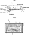
- FIG. 6 A perspective view schematically showing magnetic domain structure within an amorphous wire constituting such a conventional magneto-sensitive wire is shown in Fig. 6 .
- the magneto-sensitive wire 9 is divided into two layers of a surface layer portion 91 and a core portion 92 by a difference in magnetic domain structure.
- spins are oriented in a certain circumferential direction. Therefore, the spins as a whole are closed as circumference and as a result, no magnetic domain wall exists in the surface layer portion 91.
- the core portion 92 which lies inside the surface layer portion 91, has a multi-magnetic domain structure and a lot of magnetic domain walls exist in the core portion 92.
- magnetic domain walls exist in a boundary between the surface layer portion 91 and the core portion 92, because the direction of respective spins discontinuously varies.
- the conventional magneto-sensitive wire 9 as a whole has a magnetically composite structure.
- the magnetic domain walls existing in the multi-magnetic domain structure of the core portion 92 and those existing in the boundary between the surface layer portion 91 and the core portion 92 has caused degradation of the hysteresis characteristics of the magneto-sensitive wire 9 or a sensor employing the same.
- the present invention relates to a method of manufacturing a magneto-sensitive wire, a magneto-sensitive wire manufactured by the method and having good hysteresis characteristics which is suitable for magnetic sensors and the like, and an MI element or an MI sensor employing the same.
- the magneto-sensitive wire of the present invention can be constituted by adding one or more constituent features arbitrarily selected from the followings to the abovementioned constitution. Which embodiment is best depends on application target, required performance and so on.
- This magneto-sensitive wire is produced, for example, by suitably controlling alloy components, wire diameter and internal stress.
- An alloy to be used is a Co-Fe-Si-B alloy material preferably having zero magnetostriction.
- the wire diameter is not more than 15 ⁇ m.
- the magneto-sensitive wire of the present invention has a diameter of, for example, 0.5 to 15 ⁇ m.
- tension annealing Internal stress is controlled, for example, by applying thermal treatment to the wire with a tension applied (hereinafter referred to as “tension annealing"), applying thermal treatment to the wire with an electric current passed through. These thermal treatments are applied below a temperature at which the amorphous phase is completely changed into the crystalline phase.
- MI sensor of the present invention can obtain similar effects also by directly detecting a variation in impedance of the magneto-sensitive wire.
- the MI element or the MI sensor of the present invention exhibits such good hysteresis characteristics that hysteresis detected by the MI sensor is almost zero.
- an MI sensor using the magneto-sensitive wire of the present invention is greatly improved in linearity of output voltage characteristics with respect to applied magnetic field in a measurement range when compared to an MI sensor using a conventional magneto-sensitive wire.
- An amorphous wire of 11.6 ⁇ m in diameter having an alloy composition of Co 71.2 Fe 4.8 Si 11.8 B 12.2 (at%) and produced by an improved Taylor method was used as a specimen material of a magneto-sensitive wire according to an example of the present invention.
- This amorphous wire serving as a specimen material was subjected to thermal treatment for 7 seconds at an atmosphere temperature of 520 deg. C with a tension of 200 MPa applied (Example 1).
- amorphous wire having a spin structure in which spins are aligned in a certain circumferential direction in a surface layer portion like the surface layer portion 91 in Fig. 6 , and a multi-magnetic domain structure in an inner portion (produced by UNITIKA Ltd.).
- This amorphous wire was produced by an in-rotating-liquid spinning process and had an alloy composition of (Co 94 Fe 6 ) 72.5 Si 12.5 B 15 (at%) and a diameter of 20 ⁇ m and was subjected to tension annealing.
- amorphous wire having a reduced diameter of 13 ⁇ m was also prepared by etching the abovementioned amorphous wire used as the conventional example (Example 2).
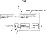
- a detection coil 3 disposed around a magneto-sensitive wire 1 through an insulator 4 (not shown) is installed on a substrate 10. Both ends of the magneto-sensitive wire 1 are connected to electrodes 51 for applying pulse current.
- the detection coil 3 is connected to electrodes 52 for detecting a voltage which varies depending on an external magnetic field.
- the magneto-sensitive wire 1 has a length of 0. 6 mm and the detection coil 3 has 15 coil turns.
- the constitution shown here is just an example and other known MI element constitutions can be employed.
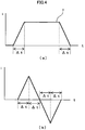
- the MI sensor 6 comprises the MI element 2, a pulse oscillation circuit 61, and a signal processing circuit 62.
- the sensor 6 operates as follows.
- High-frequency pulse current of about 50 to 250 MHz generated by the pulse oscillation circuit 61 is supplied to the magneto-sensitive wire 1 in the MI element 2. Then, due to an action of an external magnetic field and a magnetic field formed by the pulse current in a wire circumferential direction, a voltage based on rotation of the spins in the magneto-sensitive wire 1 is generated at the detection coil 3.
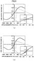
- Frequency of this voltage is calculated by first obtaining a rise time or a fall time ⁇ t in a pulse current waveform 7, as shown in Fig. 4 (a) , and then obtaining cycle time from the time ⁇ t, assuming that the time ⁇ t is one fourth of waveform cycle time, as shown in Fig. 4(b) .
- an analog switch 622 is switched (on and off) in a short time at a certain timing by a sample timing control circuit 621. This switching allows the analog switch 622 to sample a voltage corresponding to the external magnetic field and generated at the detection coil 3 and transmit the voltage to an amplifier 623. Similar operations are performed when the pulse current is interrupted (falls).
- Magneto-impedance (MI) characteristics of this example was evaluated by placing the MI sensor 6 in magnetic fields of ⁇ 2400 A/m, 10Hz and inputting pulse current of 80 mA corresponding to a frequency of 0.2 GHz to the magneto-sensitive wire 1 of the MI element 2, processing voltage signals generated at the detection coil 3 in the abovementioned signal processing circuit 62 to measure voltages of the respective magnetic fields output from the detection coil 3.
- a rise time and a fall time of the pulse current were both 1.25 ns. Although voltage was detected by using the fall of pulse current, the voltage can be detected by using the rise or both the rise and the fall.
- the magneto-sensitive wire comprises a Co-Fe-Si-B alloy, preferably having zero magnetostriction.
- the Co-Fe-Si-B alloy comprises 60 to 80 at% of Co, 3 to 7 at% of Fe, 5 to 20 at% of Si and 7 to 30 at% of B when the entire alloy composition is regarded as 100 at%. It is more preferable that the Co-Fe-Si-B alloy comprise 65 to 75 at% of Co, 4 to 6 at% of Fe, 7 to 15 at% of Si and 10 to 20 at% of B. It should be noted that an upper limit value or a lower limit value of a compositional range of each element can be any value in the abovementioned numerical value ranges.
- the magneto-sensitive wire of the present invention can contain inevitable impurities.
- the magneto-sensitive wire of the present invention comprises an amorphous wire comprising an alloy having such composition as mentioned above.
- this thermal treatment is a thermal treatment in a temperature range where the amorphous wire is not completely crystallized, in an inert gas atmosphere or a vacuum atmosphere.
- the heating temperature is 500 to 600 deg. C.
- the heating time is 4 to 10 seconds.
- the tension to be applied is 30 to 2000 MPa.
- the magneto-sensitive wire has hysteresis characteristics of not more than 7 A/m, not more than 5 A/m, or not more than 3 A/m. These levels can be regarded as substantially zero hysteresis.
- the magneto-sensitive wire has linearity of not more than 2 % F. S., not more than 1.5 % F. S., not more than 1 % F. S., or not more than 0.8 % F. S. in 30 % of an applied magnetic field range specified by applied magnetic fields corresponding to peak voltages detected by the MI sensor.
- x to y mentioned in the description of the present invention includes the lower limit value x and the upper limit value y, unless otherwise specified.
- the lower limit values and the upper limit values described in the description of the present invention can be combined arbitrarily to constitute such a range as "a to b".
- the upper limit values or the lower limit values can be replaced with any numerical value in the described numerical value ranges.
Landscapes
- Physics & Mathematics (AREA)
- Condensed Matter Physics & Semiconductors (AREA)
- General Physics & Mathematics (AREA)
- Chemical & Material Sciences (AREA)
- Engineering & Computer Science (AREA)
- Nanotechnology (AREA)
- Crystallography & Structural Chemistry (AREA)
- Hall/Mr Elements (AREA)
- Measuring Magnetic Variables (AREA)
Claims (5)
- Herstellungsverfahren eines magnetosensitiven Drahts, aufweisend:Bereitstellen eines amorphen Drahts, der eine weiche, magnetische Co-Fe-Si-B-Legierung aufweist, die 60 bis 80 Atomprozent an Co, 3 bis 7 Atomprozent an Fe, 5 bis 20 Atomprozent an Si und 7 bis 30 Atomprozent an B enthält, wenn die gesamte Legierungsmischung 100 Atomprozent ausmacht, undWärmebehandeln des amorphen Drahts in einem Temperaturbereich, in dem der amorphe Draht nicht komplett kristallisiert ist, während ein Zug in dem Bereich zwischen 30 und 2000 MPa auf den amorphen Draht ausgeübt wird,dadurch gekennzeichnet, dass der amorphe Draht in einem Temperaturbereich zwischen 500 und 600 °C wärmebehandelt wird und die Aufheizzeit für die Wärmebehandlung in einem Bereich zwischen 4 und 10 Sekunden liegt.
- Herstellungsverfahren eines magnetosensitiven Drahts nach Anspruch 1,
wobei die Wärmebehandlung in einer Inertgasatmosphäre oder in einer Vakuumatmosphäre durchgeführt wird. - Magnetosensitiver Draht, hergestellt durch ein Verfahren nach einem der Ansprüche 1 bis 2,
der einen Durchmesser in dem Bereich zwischen 0,5 und 15 µm und eine Magnetostriktion von weniger als 10-6 aufweist. - Magnetoimpedanzelement, das den magnetosensitiven Draht nach Anspruch 3 als einen Magnetdetektor beinhaltet.
- Magnetoimpedanzsensor, der das Magnetoimpedanzelement nach Anspruch 4 beinhaltet.
Applications Claiming Priority (2)
| Application Number | Priority Date | Filing Date | Title |
|---|---|---|---|
| JP2008085878 | 2008-03-28 | ||
| PCT/JP2009/001316 WO2009119081A1 (ja) | 2008-03-28 | 2009-03-25 | 感磁ワイヤ、マグネトインピーダンス素子およびマグネトインピーダンスセンサ |
Publications (3)
| Publication Number | Publication Date |
|---|---|
| EP2276082A1 EP2276082A1 (de) | 2011-01-19 |
| EP2276082A4 EP2276082A4 (de) | 2012-01-25 |
| EP2276082B1 true EP2276082B1 (de) | 2016-06-22 |
Family
ID=41113292
Family Applications (1)
| Application Number | Title | Priority Date | Filing Date |
|---|---|---|---|
| EP09724160.8A Active EP2276082B1 (de) | 2008-03-28 | 2009-03-25 | Magnetempfindlicher draht, magnetimpedanzelement und magnetimpedanzsensor |
Country Status (7)
| Country | Link |
|---|---|
| US (1) | US8610427B2 (de) |
| EP (1) | EP2276082B1 (de) |
| JP (1) | JP4650591B2 (de) |
| KR (1) | KR101475551B1 (de) |
| CN (2) | CN103454601B (de) |
| ES (1) | ES2584513T3 (de) |
| WO (1) | WO2009119081A1 (de) |
Families Citing this family (26)
| Publication number | Priority date | Publication date | Assignee | Title |
|---|---|---|---|---|
| US8686722B2 (en) * | 2011-08-26 | 2014-04-01 | National Semiconductor Corporation | Semiconductor fluxgate magnetometer |
| US8680854B2 (en) * | 2011-12-01 | 2014-03-25 | Texas Instruments Incorporated | Semiconductor GMI magnetometer |
| KR20150065679A (ko) * | 2012-10-04 | 2015-06-15 | 아이치 세이꼬 가부시키 가이샤 | 마그네토 임피던스 소자 및 그 제조 방법 |
| JP5678358B2 (ja) | 2013-01-25 | 2015-03-04 | マグネデザイン株式会社 | 磁気検出装置 |
| JP6281677B2 (ja) * | 2013-03-08 | 2018-02-21 | 国立大学法人名古屋大学 | 磁気計測装置 |
| JP6222351B2 (ja) * | 2014-05-09 | 2017-11-01 | 愛知製鋼株式会社 | 磁気検出装置およびその製造方法 |
| JP5839527B1 (ja) | 2015-02-16 | 2016-01-06 | マグネデザイン株式会社 | 超高感度マイクロ磁気センサ |
| JP6398830B2 (ja) | 2015-03-26 | 2018-10-03 | 愛知製鋼株式会社 | 磁気インピーダンスセンサ |
| JP6210084B2 (ja) * | 2015-04-21 | 2017-10-11 | 愛知製鋼株式会社 | 高精度測定可能な磁気インピーダンスセンサ用感磁ワイヤの製造方法 |
| JP6036938B1 (ja) | 2015-08-05 | 2016-11-30 | 愛知製鋼株式会社 | 磁気検出装置 |
| TWI578547B (zh) * | 2015-09-10 | 2017-04-11 | 旺玖科技股份有限公司 | 電磁阻抗感測元件及其製作方法 |
| JP5991634B1 (ja) * | 2015-12-18 | 2016-09-14 | マグネデザイン株式会社 | 磁気検出装置 |
| EP3415691A4 (de) | 2016-02-10 | 2019-10-09 | Aichi Steel Corporation | Verfahren zur installation eines magnetischen markers und arbeitsfahrzeugsystem |
| SG11201806864UA (en) | 2016-02-16 | 2018-09-27 | Aichi Steel Corp | Work vehicle system and magnetic marker work method |
| JP2017181379A (ja) * | 2016-03-31 | 2017-10-05 | フジデノロ株式会社 | 磁気検出素子及び磁気インピーダンスセンサ |
| JP7012421B2 (ja) | 2016-06-17 | 2022-01-28 | 愛知製鋼株式会社 | 磁気マーカ及びマーカシステム |
| JP6816445B2 (ja) * | 2016-10-21 | 2021-01-20 | 愛知製鋼株式会社 | 高精度測定可能な磁気センサ用感磁体の製造方法 |
| US10253392B2 (en) | 2017-06-14 | 2019-04-09 | Aichi Steel Corporation | Apparatus for treating magnetic wire and method for treating the same |
| JP7262885B2 (ja) * | 2017-06-16 | 2023-04-24 | 朝日インテック株式会社 | 超高感度マイクロ磁気センサ |
| JP6428884B1 (ja) | 2017-09-11 | 2018-11-28 | 愛知製鋼株式会社 | 磁気センサ用感磁ワイヤおよびその製造方法 |
| JP6605570B2 (ja) * | 2017-12-27 | 2019-11-13 | Tdk株式会社 | 磁気センサ |
| CN108519563A (zh) * | 2018-04-02 | 2018-09-11 | 南京麦科尼传感技术有限公司 | 一种基于非晶丝的高分辨率正交磁通门三轴磁强计及其制造技术 |
| CN108983123A (zh) * | 2018-07-20 | 2018-12-11 | 常州微磁非晶丝传感器有限公司 | 一种高分辨率非晶丝正交磁通门传感器及其制造技术 |
| JP6791227B2 (ja) * | 2018-11-02 | 2020-11-25 | 愛知製鋼株式会社 | 磁気センサ用感磁ワイヤおよびその製造方法 |
| JP7529969B2 (ja) | 2020-03-24 | 2024-08-07 | 愛知製鋼株式会社 | 感磁ワイヤおよびその製造方法 |
| JP6924453B1 (ja) * | 2020-08-26 | 2021-08-25 | マグネデザイン株式会社 | Gsrセンサ素子の製造方法 |
Family Cites Families (12)
| Publication number | Priority date | Publication date | Assignee | Title |
|---|---|---|---|---|
| JP3197414B2 (ja) | 1993-12-22 | 2001-08-13 | 科学技術振興事業団 | 磁気インピーダンス効果素子 |
| EP1134731A3 (de) * | 2000-03-16 | 2002-05-29 | Toda Kogyo Corporation | Diskrete magnetische Dünnfilmelemente mit senkrechter Magnetisierung |
| JP2001296127A (ja) * | 2000-04-13 | 2001-10-26 | Aichi Steel Works Ltd | 磁場検出装置 |
| JP2002374016A (ja) * | 2001-06-14 | 2002-12-26 | Toyota Motor Corp | 磁気検出素子 |
| JP2005227297A (ja) | 2002-02-19 | 2005-08-25 | Aichi Steel Works Ltd | 電磁コイル付マグネト・インピーダンス・センサ素子 |
| US7224161B2 (en) * | 2002-02-19 | 2007-05-29 | Aichi Steel Corporation | Magnet with electromagnetic coil/impedance/sensor element |
| JP3771228B2 (ja) * | 2002-08-12 | 2006-04-26 | Tdk株式会社 | 磁気光学光部品 |
| JP4403264B2 (ja) | 2003-06-05 | 2010-01-27 | 独立行政法人産業技術総合研究所 | 環状単磁区構造微小磁性体およびその製造方法又はそれを用いた磁気記録素子 |
| JP2005062000A (ja) | 2003-08-12 | 2005-03-10 | Sankyo Seiki Mfg Co Ltd | 磁気検出素子および磁気検出回路 |
| JP3801194B2 (ja) * | 2003-08-25 | 2006-07-26 | 愛知製鋼株式会社 | 磁気センサ |
| JP4529783B2 (ja) * | 2005-04-25 | 2010-08-25 | 愛知製鋼株式会社 | マグネト・インピーダンス・センサ素子 |
| JP5349840B2 (ja) | 2007-06-25 | 2013-11-20 | キヤノン株式会社 | 磁気センサ素子及びそれを備える検出装置 |
-
2009
- 2009-03-25 ES ES09724160.8T patent/ES2584513T3/es active Active
- 2009-03-25 CN CN201310317044.2A patent/CN103454601B/zh not_active Expired - Fee Related
- 2009-03-25 CN CN2009801111189A patent/CN101981719A/zh active Pending
- 2009-03-25 JP JP2010505344A patent/JP4650591B2/ja active Active
- 2009-03-25 WO PCT/JP2009/001316 patent/WO2009119081A1/ja not_active Ceased
- 2009-03-25 EP EP09724160.8A patent/EP2276082B1/de active Active
- 2009-03-25 US US12/736,298 patent/US8610427B2/en not_active Expired - Fee Related
- 2009-03-25 KR KR1020107024036A patent/KR101475551B1/ko active Active
Non-Patent Citations (6)
| Title |
|---|
| CHEN D-X ET AL: "Circular susceptibilities of CoFeSiB amorphous wires determined by inductance and second harmonic longitudinal magnetization", JOURNAL OF APPLIED PHYSICS, AMERICAN INSTITUTE OF PHYSICS, 2 HUNTINGTON QUADRANGLE, MELVILLE, NY 11747, vol. 93, no. 10, 15 May 2003 (2003-05-15), pages 6195 - 6198, XP012057809, ISSN: 0021-8979, DOI: 10.1063/1.1568522 * |
| CHIRIAC H ET AL: "Effect of Mo and Nb additions on the magnetic properties of CoFeSiB amorphous wires", JOURNAL OF NON-CRYSTALLINE SOLIDS, NORTH-HOLLAND PHYSICS PUBLISHING. AMSTERDAM, NL, vol. 250-252, 1 August 1999 (1999-08-01), pages 762 - 765, XP004183357, ISSN: 0022-3093, DOI: 10.1016/S0022-3093(99)00175-1 * |
| FREIJO J J ET AL: "Matteucci and inverse Wiedemann effects in amorphous wires with enhanced circumferential domains", JOURNAL OF APPLIED PHYSICS, AMERICAN INSTITUTE OF PHYSICS, 2 HUNTINGTON QUADRANGLE, MELVILLE, NY 11747, vol. 85, no. 8, 15 April 1999 (1999-04-15), pages 5450 - 5452, XP012047473, ISSN: 0021-8979, DOI: 10.1063/1.369972 * |
| HUMPHREY ET AL: "Applications of amorphous wire", MATERIALS SCIENCE AND ENGINEERING A: STRUCTURAL MATERIALS:PROPERTIES, MICROSTRUCTURE & PROCESSING, LAUSANNE, CH, vol. 179-180, 1 May 1994 (1994-05-01), pages 66 - 71, XP025877865, ISSN: 0921-5093, [retrieved on 19940501], DOI: 10.1016/0921-5093(94)90166-X * |
| MOHRI K ET AL: "Phase Modulation Device Using Amorphous Short Wire", IEEE TRANSLATION JOURNAL ON MAGNETICS IN JAPAN, IEEE INC, NEW YORK, US, vol. 6, no. 6, 1 November 1994 (1994-11-01), pages 61 - 65, XP011231235, ISSN: 0882-4959 * |
| ZHAO Z J ET AL: "Structure and magnetic properties of iron/cobalt-based glass-covered microwires", PHYSICA SCRIPTA, INSTITUTE OF PHYSICS PUBLISHING, BRISTOL, GB, vol. 2007, no. T129, 1 December 2007 (2007-12-01), pages 153 - 156, XP020131021, ISSN: 1402-4896 * |
Also Published As
| Publication number | Publication date |
|---|---|
| EP2276082A4 (de) | 2012-01-25 |
| US20110080164A1 (en) | 2011-04-07 |
| JPWO2009119081A1 (ja) | 2011-07-21 |
| US8610427B2 (en) | 2013-12-17 |
| KR20110002852A (ko) | 2011-01-10 |
| WO2009119081A1 (ja) | 2009-10-01 |
| KR101475551B1 (ko) | 2014-12-22 |
| EP2276082A1 (de) | 2011-01-19 |
| CN103454601B (zh) | 2016-05-18 |
| CN103454601A (zh) | 2013-12-18 |
| ES2584513T3 (es) | 2016-09-28 |
| CN101981719A (zh) | 2011-02-23 |
| JP4650591B2 (ja) | 2011-03-16 |
Similar Documents
| Publication | Publication Date | Title |
|---|---|---|
| EP2276082B1 (de) | Magnetempfindlicher draht, magnetimpedanzelement und magnetimpedanzsensor | |
| US8350565B2 (en) | Ultra-sensitive magnetoimpedance sensor | |
| Vázquez | Soft magnetic wires | |
| Vázquez et al. | Magneto-impedance in glass-coated CoMnSiB amorphous microwires | |
| Jantaratana et al. | Effects of thickness and heat treatments on giant magnetoimpedance of electrodeposited cobalt on silver wires | |
| El Kammouni et al. | Temperature dependence of microwave absorption phenomena in single and biphase soft magnetic microwires | |
| Hu et al. | Diameter dependence of the giant magnetoimpedance in hard-drawn CoFeSiB amorphous wires | |
| Ripka et al. | Sensitivity and noise of wire-core transverse fluxgate | |
| Corodeanu et al. | Effect of in situ glass removal on the magnetic switching in amorphous microwires | |
| Phan et al. | Giant magnetoimpedance effect in Co70Fe5Si15B10 and Co70Fe5Si15Nb2. 2Cu0. 8B7 ribbons | |
| Zhou et al. | Transverse, longitudinal and perpendicular giant magnetoimpedance effects in a compact multiturn meander NiFe/Cu/NiFe trilayer film sensor | |
| Yu et al. | Micromachined two-dimensional weak magnetic field sensors of soft magnetic film/planar coil laminated | |
| Kikuchi et al. | Magneto-Impedance of Micromachined Thin Films Less Than 100$\mu $ m in Length | |
| Choi et al. | Effects of lateral dimensions of the magnetic thin films on the characteristics of thin-film type orthogonal fluxgate sensors | |
| Pal et al. | The effect of magnetoelastic interaction on the GMI behaviour of Fe-, Co-and Co–Fe-based amorphous wires | |
| Le et al. | A study of giant magnetoimpedance effect and magnetic response in micro-patterned F/Ag/F magnetic ribbon structures (F= Co-rich amorphous ribbon) | |
| Lv et al. | STRESS-INDUCED ASYMMETRIC MAGNETOIMPEDANCE EFFECT IN Ni 8 0 Fe 2 0/Cu COMPOSITE WIRES | |
| Sanchez et al. | Torsion annealing influence on the impedance behaviour in amorphous FeSiB and CoSiB wires | |
| Choi et al. | Orthogonal fluxgate sensor fabricated with a Co-based amorphous wire embedded onto surface of alumina substrate | |
| Wu et al. | Resonance enhancement of the giant magnetoimpedance effect in glass-coated microwires with outer conductive layer | |
| Borza et al. | Magnetic properties of CoFeSiB/(Co, CoPtRh) multilayer microwires | |
| Mitrović et al. | Penetration Depth and Magnetoimpedance Effect in CoFeSiB and FeNbCuSiB Amorphous Wires | |
| Kocaman et al. | Developing Miniaturized Orthogonal Fluxgate Sensors | |
| Chiriac | Giant magneto-impedance effect in amorphous wires | |
| Zheng | Influence of Frequency and Bias Current on Asymmetrical GMI Effect in Co71. 8 Fe4. 9 Nb0. 8 Si7. 5 B15 Amorphous Glass-Covered Wires |
Legal Events
| Date | Code | Title | Description |
|---|---|---|---|
| PUAI | Public reference made under article 153(3) epc to a published international application that has entered the european phase |
Free format text: ORIGINAL CODE: 0009012 |
|
| 17P | Request for examination filed |
Effective date: 20101028 |
|
| AK | Designated contracting states |
Kind code of ref document: A1 Designated state(s): AT BE BG CH CY CZ DE DK EE ES FI FR GB GR HR HU IE IS IT LI LT LU LV MC MK MT NL NO PL PT RO SE SI SK TR |
|
| AX | Request for extension of the european patent |
Extension state: AL BA RS |
|
| DAX | Request for extension of the european patent (deleted) | ||
| REG | Reference to a national code |
Ref country code: DE Ref legal event code: R079 Ref document number: 602009039323 Country of ref document: DE Free format text: PREVIOUS MAIN CLASS: H01L0043000000 Ipc: G01R0033060000 |
|
| A4 | Supplementary search report drawn up and despatched |
Effective date: 20111228 |
|
| RIC1 | Information provided on ipc code assigned before grant |
Ipc: G01R 33/06 20060101AFI20111221BHEP Ipc: H01L 43/08 20060101ALI20111221BHEP |
|
| 17Q | First examination report despatched |
Effective date: 20140107 |
|
| GRAP | Despatch of communication of intention to grant a patent |
Free format text: ORIGINAL CODE: EPIDOSNIGR1 |
|
| INTG | Intention to grant announced |
Effective date: 20160203 |
|
| GRAS | Grant fee paid |
Free format text: ORIGINAL CODE: EPIDOSNIGR3 |
|
| GRAA | (expected) grant |
Free format text: ORIGINAL CODE: 0009210 |
|
| AK | Designated contracting states |
Kind code of ref document: B1 Designated state(s): AT BE BG CH CY CZ DE DK EE ES FI FR GB GR HR HU IE IS IT LI LT LU LV MC MK MT NL NO PL PT RO SE SI SK TR |
|
| REG | Reference to a national code |
Ref country code: GB Ref legal event code: FG4D |
|
| REG | Reference to a national code |
Ref country code: CH Ref legal event code: EP |
|
| REG | Reference to a national code |
Ref country code: IE Ref legal event code: FG4D |
|
| REG | Reference to a national code |
Ref country code: AT Ref legal event code: REF Ref document number: 807978 Country of ref document: AT Kind code of ref document: T Effective date: 20160715 |
|
| REG | Reference to a national code |
Ref country code: DE Ref legal event code: R096 Ref document number: 602009039323 Country of ref document: DE |
|
| REG | Reference to a national code |
Ref country code: ES Ref legal event code: FG2A Ref document number: 2584513 Country of ref document: ES Kind code of ref document: T3 Effective date: 20160928 |
|
| REG | Reference to a national code |
Ref country code: LT Ref legal event code: MG4D |
|
| REG | Reference to a national code |
Ref country code: NL Ref legal event code: MP Effective date: 20160622 |
|
| PG25 | Lapsed in a contracting state [announced via postgrant information from national office to epo] |
Ref country code: LT Free format text: LAPSE BECAUSE OF FAILURE TO SUBMIT A TRANSLATION OF THE DESCRIPTION OR TO PAY THE FEE WITHIN THE PRESCRIBED TIME-LIMIT Effective date: 20160622 Ref country code: NO Free format text: LAPSE BECAUSE OF FAILURE TO SUBMIT A TRANSLATION OF THE DESCRIPTION OR TO PAY THE FEE WITHIN THE PRESCRIBED TIME-LIMIT Effective date: 20160922 Ref country code: FI Free format text: LAPSE BECAUSE OF FAILURE TO SUBMIT A TRANSLATION OF THE DESCRIPTION OR TO PAY THE FEE WITHIN THE PRESCRIBED TIME-LIMIT Effective date: 20160622 |
|
| REG | Reference to a national code |
Ref country code: AT Ref legal event code: MK05 Ref document number: 807978 Country of ref document: AT Kind code of ref document: T Effective date: 20160622 |
|
| PG25 | Lapsed in a contracting state [announced via postgrant information from national office to epo] |
Ref country code: SE Free format text: LAPSE BECAUSE OF FAILURE TO SUBMIT A TRANSLATION OF THE DESCRIPTION OR TO PAY THE FEE WITHIN THE PRESCRIBED TIME-LIMIT Effective date: 20160622 Ref country code: GR Free format text: LAPSE BECAUSE OF FAILURE TO SUBMIT A TRANSLATION OF THE DESCRIPTION OR TO PAY THE FEE WITHIN THE PRESCRIBED TIME-LIMIT Effective date: 20160923 Ref country code: LV Free format text: LAPSE BECAUSE OF FAILURE TO SUBMIT A TRANSLATION OF THE DESCRIPTION OR TO PAY THE FEE WITHIN THE PRESCRIBED TIME-LIMIT Effective date: 20160622 Ref country code: NL Free format text: LAPSE BECAUSE OF FAILURE TO SUBMIT A TRANSLATION OF THE DESCRIPTION OR TO PAY THE FEE WITHIN THE PRESCRIBED TIME-LIMIT Effective date: 20160622 Ref country code: HR Free format text: LAPSE BECAUSE OF FAILURE TO SUBMIT A TRANSLATION OF THE DESCRIPTION OR TO PAY THE FEE WITHIN THE PRESCRIBED TIME-LIMIT Effective date: 20160622 |
|
| PG25 | Lapsed in a contracting state [announced via postgrant information from national office to epo] |
Ref country code: RO Free format text: LAPSE BECAUSE OF FAILURE TO SUBMIT A TRANSLATION OF THE DESCRIPTION OR TO PAY THE FEE WITHIN THE PRESCRIBED TIME-LIMIT Effective date: 20160622 Ref country code: IS Free format text: LAPSE BECAUSE OF FAILURE TO SUBMIT A TRANSLATION OF THE DESCRIPTION OR TO PAY THE FEE WITHIN THE PRESCRIBED TIME-LIMIT Effective date: 20161022 Ref country code: SK Free format text: LAPSE BECAUSE OF FAILURE TO SUBMIT A TRANSLATION OF THE DESCRIPTION OR TO PAY THE FEE WITHIN THE PRESCRIBED TIME-LIMIT Effective date: 20160622 Ref country code: CZ Free format text: LAPSE BECAUSE OF FAILURE TO SUBMIT A TRANSLATION OF THE DESCRIPTION OR TO PAY THE FEE WITHIN THE PRESCRIBED TIME-LIMIT Effective date: 20160622 Ref country code: EE Free format text: LAPSE BECAUSE OF FAILURE TO SUBMIT A TRANSLATION OF THE DESCRIPTION OR TO PAY THE FEE WITHIN THE PRESCRIBED TIME-LIMIT Effective date: 20160622 Ref country code: IT Free format text: LAPSE BECAUSE OF FAILURE TO SUBMIT A TRANSLATION OF THE DESCRIPTION OR TO PAY THE FEE WITHIN THE PRESCRIBED TIME-LIMIT Effective date: 20160622 |
|
| PG25 | Lapsed in a contracting state [announced via postgrant information from national office to epo] |
Ref country code: BE Free format text: LAPSE BECAUSE OF FAILURE TO SUBMIT A TRANSLATION OF THE DESCRIPTION OR TO PAY THE FEE WITHIN THE PRESCRIBED TIME-LIMIT Effective date: 20160622 Ref country code: AT Free format text: LAPSE BECAUSE OF FAILURE TO SUBMIT A TRANSLATION OF THE DESCRIPTION OR TO PAY THE FEE WITHIN THE PRESCRIBED TIME-LIMIT Effective date: 20160622 Ref country code: PT Free format text: LAPSE BECAUSE OF FAILURE TO SUBMIT A TRANSLATION OF THE DESCRIPTION OR TO PAY THE FEE WITHIN THE PRESCRIBED TIME-LIMIT Effective date: 20161024 Ref country code: PL Free format text: LAPSE BECAUSE OF FAILURE TO SUBMIT A TRANSLATION OF THE DESCRIPTION OR TO PAY THE FEE WITHIN THE PRESCRIBED TIME-LIMIT Effective date: 20160622 |
|
| REG | Reference to a national code |
Ref country code: FR Ref legal event code: PLFP Year of fee payment: 9 |
|
| REG | Reference to a national code |
Ref country code: DE Ref legal event code: R097 Ref document number: 602009039323 Country of ref document: DE |
|
| PLBE | No opposition filed within time limit |
Free format text: ORIGINAL CODE: 0009261 |
|
| STAA | Information on the status of an ep patent application or granted ep patent |
Free format text: STATUS: NO OPPOSITION FILED WITHIN TIME LIMIT |
|
| 26N | No opposition filed |
Effective date: 20170323 |
|
| PG25 | Lapsed in a contracting state [announced via postgrant information from national office to epo] |
Ref country code: DK Free format text: LAPSE BECAUSE OF FAILURE TO SUBMIT A TRANSLATION OF THE DESCRIPTION OR TO PAY THE FEE WITHIN THE PRESCRIBED TIME-LIMIT Effective date: 20160622 |
|
| PG25 | Lapsed in a contracting state [announced via postgrant information from national office to epo] |
Ref country code: SI Free format text: LAPSE BECAUSE OF FAILURE TO SUBMIT A TRANSLATION OF THE DESCRIPTION OR TO PAY THE FEE WITHIN THE PRESCRIBED TIME-LIMIT Effective date: 20160622 |
|
| REG | Reference to a national code |
Ref country code: CH Ref legal event code: PL |
|
| PG25 | Lapsed in a contracting state [announced via postgrant information from national office to epo] |
Ref country code: MC Free format text: LAPSE BECAUSE OF FAILURE TO SUBMIT A TRANSLATION OF THE DESCRIPTION OR TO PAY THE FEE WITHIN THE PRESCRIBED TIME-LIMIT Effective date: 20160622 |
|
| REG | Reference to a national code |
Ref country code: IE Ref legal event code: MM4A |
|
| PG25 | Lapsed in a contracting state [announced via postgrant information from national office to epo] |
Ref country code: LU Free format text: LAPSE BECAUSE OF NON-PAYMENT OF DUE FEES Effective date: 20170325 |
|
| PG25 | Lapsed in a contracting state [announced via postgrant information from national office to epo] |
Ref country code: LI Free format text: LAPSE BECAUSE OF NON-PAYMENT OF DUE FEES Effective date: 20170331 Ref country code: CH Free format text: LAPSE BECAUSE OF NON-PAYMENT OF DUE FEES Effective date: 20170331 Ref country code: IE Free format text: LAPSE BECAUSE OF NON-PAYMENT OF DUE FEES Effective date: 20170325 |
|
| REG | Reference to a national code |
Ref country code: FR Ref legal event code: PLFP Year of fee payment: 10 |
|
| PG25 | Lapsed in a contracting state [announced via postgrant information from national office to epo] |
Ref country code: MT Free format text: LAPSE BECAUSE OF NON-PAYMENT OF DUE FEES Effective date: 20170325 |
|
| PG25 | Lapsed in a contracting state [announced via postgrant information from national office to epo] |
Ref country code: HU Free format text: LAPSE BECAUSE OF FAILURE TO SUBMIT A TRANSLATION OF THE DESCRIPTION OR TO PAY THE FEE WITHIN THE PRESCRIBED TIME-LIMIT; INVALID AB INITIO Effective date: 20090325 |
|
| PG25 | Lapsed in a contracting state [announced via postgrant information from national office to epo] |
Ref country code: BG Free format text: LAPSE BECAUSE OF FAILURE TO SUBMIT A TRANSLATION OF THE DESCRIPTION OR TO PAY THE FEE WITHIN THE PRESCRIBED TIME-LIMIT Effective date: 20160622 |
|
| PG25 | Lapsed in a contracting state [announced via postgrant information from national office to epo] |
Ref country code: CY Free format text: LAPSE BECAUSE OF NON-PAYMENT OF DUE FEES Effective date: 20160622 |
|
| PG25 | Lapsed in a contracting state [announced via postgrant information from national office to epo] |
Ref country code: MK Free format text: LAPSE BECAUSE OF FAILURE TO SUBMIT A TRANSLATION OF THE DESCRIPTION OR TO PAY THE FEE WITHIN THE PRESCRIBED TIME-LIMIT Effective date: 20160622 |
|
| PG25 | Lapsed in a contracting state [announced via postgrant information from national office to epo] |
Ref country code: TR Free format text: LAPSE BECAUSE OF FAILURE TO SUBMIT A TRANSLATION OF THE DESCRIPTION OR TO PAY THE FEE WITHIN THE PRESCRIBED TIME-LIMIT Effective date: 20160622 |
|
| P01 | Opt-out of the competence of the unified patent court (upc) registered |
Effective date: 20230413 |
|
| PGFP | Annual fee paid to national office [announced via postgrant information from national office to epo] |
Ref country code: DE Payment date: 20240320 Year of fee payment: 16 Ref country code: GB Payment date: 20240320 Year of fee payment: 16 |
|
| PGFP | Annual fee paid to national office [announced via postgrant information from national office to epo] |
Ref country code: FR Payment date: 20240322 Year of fee payment: 16 |
|
| PGFP | Annual fee paid to national office [announced via postgrant information from national office to epo] |
Ref country code: ES Payment date: 20240426 Year of fee payment: 16 |
|
| REG | Reference to a national code |
Ref country code: DE Ref legal event code: R119 Ref document number: 602009039323 Country of ref document: DE |
|
| GBPC | Gb: european patent ceased through non-payment of renewal fee |
Effective date: 20250325 |
|
| PG25 | Lapsed in a contracting state [announced via postgrant information from national office to epo] |
Ref country code: DE Free format text: LAPSE BECAUSE OF NON-PAYMENT OF DUE FEES Effective date: 20251001 |
|
| PG25 | Lapsed in a contracting state [announced via postgrant information from national office to epo] |
Ref country code: GB Free format text: LAPSE BECAUSE OF NON-PAYMENT OF DUE FEES Effective date: 20250325 |
|
| PG25 | Lapsed in a contracting state [announced via postgrant information from national office to epo] |
Ref country code: FR Free format text: LAPSE BECAUSE OF NON-PAYMENT OF DUE FEES Effective date: 20250331 |