EP2276173A2 - Treiber für einen Leistungstransistor - Google Patents
Treiber für einen Leistungstransistor Download PDFInfo
- Publication number
- EP2276173A2 EP2276173A2 EP10165936A EP10165936A EP2276173A2 EP 2276173 A2 EP2276173 A2 EP 2276173A2 EP 10165936 A EP10165936 A EP 10165936A EP 10165936 A EP10165936 A EP 10165936A EP 2276173 A2 EP2276173 A2 EP 2276173A2
- Authority
- EP
- European Patent Office
- Prior art keywords
- voltage
- transistor
- gate
- circuit
- jfet
- Prior art date
- Legal status (The legal status is an assumption and is not a legal conclusion. Google has not performed a legal analysis and makes no representation as to the accuracy of the status listed.)
- Granted
Links
- 239000003990 capacitor Substances 0.000 claims description 30
- 230000006641 stabilisation Effects 0.000 claims description 2
- 238000011105 stabilization Methods 0.000 claims description 2
- 239000008186 active pharmaceutical agent Substances 0.000 description 7
- 230000005669 field effect Effects 0.000 description 3
- 229910002601 GaN Inorganic materials 0.000 description 2
- JMASRVWKEDWRBT-UHFFFAOYSA-N Gallium nitride Chemical compound [Ga]#N JMASRVWKEDWRBT-UHFFFAOYSA-N 0.000 description 2
- 230000000694 effects Effects 0.000 description 2
- 239000000463 material Substances 0.000 description 2
- HBMJWWWQQXIZIP-UHFFFAOYSA-N silicon carbide Chemical compound [Si+]#[C-] HBMJWWWQQXIZIP-UHFFFAOYSA-N 0.000 description 2
- 229910010271 silicon carbide Inorganic materials 0.000 description 2
- 208000032365 Electromagnetic interference Diseases 0.000 description 1
- 238000013459 approach Methods 0.000 description 1
- 230000033228 biological regulation Effects 0.000 description 1
- 230000000903 blocking effect Effects 0.000 description 1
- 238000006243 chemical reaction Methods 0.000 description 1
- 238000011084 recovery Methods 0.000 description 1
- 230000002787 reinforcement Effects 0.000 description 1
Images

Classifications
-
- H—ELECTRICITY
- H03—ELECTRONIC CIRCUITRY
- H03K—PULSE TECHNIQUE
- H03K17/00—Electronic switching or gating, i.e. not by contact-making and –breaking
- H03K17/16—Modifications for eliminating interference voltages or currents
- H03K17/161—Modifications for eliminating interference voltages or currents in field-effect transistor switches
- H03K17/162—Modifications for eliminating interference voltages or currents in field-effect transistor switches without feedback from the output circuit to the control circuit
- H03K17/163—Soft switching
-
- H—ELECTRICITY
- H03—ELECTRONIC CIRCUITRY
- H03K—PULSE TECHNIQUE
- H03K17/00—Electronic switching or gating, i.e. not by contact-making and –breaking
- H03K17/08—Modifications for protecting switching circuit against overcurrent or overvoltage
- H03K17/081—Modifications for protecting switching circuit against overcurrent or overvoltage without feedback from the output circuit to the control circuit
- H03K17/0812—Modifications for protecting switching circuit against overcurrent or overvoltage without feedback from the output circuit to the control circuit by measures taken in the control circuit
- H03K17/08122—Modifications for protecting switching circuit against overcurrent or overvoltage without feedback from the output circuit to the control circuit by measures taken in the control circuit in field-effect transistor switches
Definitions
- the present invention relates to a device for controlling a power transistor, more particularly a junction field effect transistor of JFET (Junction Field Effect Transistor) type.
- the JFET transistor will for example be made of a high band gap energy material such as silicon carbide or gallium nitride. This type of transistor can in particular be used in a PWM (Pulse Width Modulation).
- IGBT type Insulated Gate Bipolar Transistor
- the main problem to be solved is to be able to control the switching speed of the transistor. For this, it is necessary to be able to control independently of each other the variation of the current as a function of time (di / dt) and the variation of the voltage as a function of time (dV / dt).
- the goal is for example to reduce the di / dt and increase the dV / dt.
- the known commands are not satisfactory.
- the object of the invention is to provide a control device of a JFET type transistor having optimized performance in order to reduce switching losses and electromagnetic interference during the conduction of the transistor.
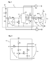
- the limiting circuit comprises an input on which is applied the voltage across a capacitor and an output on which is generated the reference gate-source voltage.
- the limiting circuit comprises a bipolar transistor and means for comparing the gate-source voltage of the JFET transistor and the predetermined maximum value.
- the limiting circuit comprises a diode and in that the maximum value is determined by the sum of the conduction threshold voltage of the bipolar transistor and the conduction threshold voltage of the diode.
- the voltage generating circuit comprises a series-connected resistor, inductor and capacitor, forming an RLC circuit connected between the output of an input circuit and the source of the JFET transistor and a clamping diode. parallel connection of the capacitor of the RLC circuit between an input of the limiting circuit and the source of the JFET transistor.
- the voltage generating circuit comprises two bipolar transistors in series, the two bases of which are interconnected and connected to the output of the limiting circuit.
- the device comprises a gate resistor connected between the gate of the transistor and the output of the voltage generating circuit.
- the device comprises a diode and a capacitor connected in series between a first input of the limiting circuit and the ground and a stabilization diode connected in parallel with the capacitor.
- the invention also relates to a power converter comprising an inverter stage comprising a plurality of JFET type transistors, each JFET transistor being controlled by a control device as defined above.
- the control device of the invention makes it possible to independently control the current variation as a function of the time that passes through the transistor and therefore the electromagnetic interferences generated by this variation, as well as the voltage variation between the drain and the source of the transistor, and therefore the switching losses.
- the controlled JFET transistor will preferably be manufactured in a high band gap material, for example of silicon carbide or gallium nitride, in order to have a low resistance to passing state (R DSon ), so to generate limited losses, and to withstand significant voltages (greater than 600 V).
- a high band gap material for example of silicon carbide or gallium nitride
- the input circuit 10 is for generating a control signal on the gate of the JFET transistor. It comprises a diode D and two switches S1, S2 in series. The output of the input circuit 10 is connected to the point between the two switches.
- the input circuit 10 is intended to generate a supply input voltage V GG which can take a positive value designated V CC , for example equal to + 5V to control the turning on of the JFET and a negative value designated V EE , ranging from -15V to -20V, to control the shutdown of the JFET transistor.
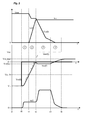
- the gate-source voltage V GS continues its increase by following the progression of the reference voltage V REF .
- the gate-source voltage V GS reaches the maximum value V GS_max , the gate-source voltage V GS must be limited so as not to damage the component.
- the reference voltage V REF is reduced to the maximum value V GS_max so as to cap the gate-source voltage to the maximum value V GS_max .
Landscapes
- Power Conversion In General (AREA)
- Electronic Switches (AREA)
- Control Of Electrical Variables (AREA)
Applications Claiming Priority (1)
| Application Number | Priority Date | Filing Date | Title |
|---|---|---|---|
| FR0954681A FR2947973B1 (fr) | 2009-07-07 | 2009-07-07 | Dispositif de commande d'un transistor de puissance |
Publications (3)
| Publication Number | Publication Date |
|---|---|
| EP2276173A2 true EP2276173A2 (de) | 2011-01-19 |
| EP2276173A3 EP2276173A3 (de) | 2012-03-21 |
| EP2276173B1 EP2276173B1 (de) | 2014-02-26 |
Family
ID=41346155
Family Applications (1)
| Application Number | Title | Priority Date | Filing Date |
|---|---|---|---|
| EP10165936.5A Not-in-force EP2276173B1 (de) | 2009-07-07 | 2010-06-15 | Treiber für einen Leistungstransistor |
Country Status (6)
| Country | Link |
|---|---|
| US (1) | US8427226B2 (de) |
| EP (1) | EP2276173B1 (de) |
| JP (1) | JP5675190B2 (de) |
| CN (1) | CN101944837B (de) |
| ES (1) | ES2453046T3 (de) |
| FR (1) | FR2947973B1 (de) |
Families Citing this family (15)
| Publication number | Priority date | Publication date | Assignee | Title |
|---|---|---|---|---|
| US20110124729A1 (en) * | 2009-11-26 | 2011-05-26 | Basf Se | Use of highly-branched polyesters in cosmetic and dermatological formulations |
| US8779807B2 (en) * | 2012-08-27 | 2014-07-15 | Avago Technologies General Ip (Singapore) Pte. Ltd. | Method, system, and apparatus for efficiently driving a transistor with a booster in voltage supply |
| CN103856046A (zh) * | 2012-11-30 | 2014-06-11 | 杰力科技股份有限公司 | 降压式电压转换装置 |
| JP6001445B2 (ja) * | 2012-12-27 | 2016-10-05 | 株式会社東芝 | 駆動回路および半導体装置 |
| PL3317967T3 (pl) * | 2015-06-30 | 2020-11-02 | Fronius International Gmbh | Układ połączeń do sterowania tranzystorem |
| US9887537B2 (en) * | 2015-06-30 | 2018-02-06 | Microsoft Technology Licensing, Llc | Analog limit on digitally set pulse widths |
| DE102015221636A1 (de) * | 2015-11-04 | 2017-05-04 | Robert Bosch Gmbh | Verfahren zum Betreiben eines Metall-Oxid-Halbleiter-Feldeffekttransistors |
| CN105846665B (zh) * | 2016-04-28 | 2018-12-07 | 南京航空航天大学 | 一种具有自保护功能的常通型SiC JFET驱动电路 |
| DE102017119600B4 (de) * | 2017-08-25 | 2019-06-27 | Infineon Technologies Austria Ag | Verfahren zum Ansteuern eines Transistorbauelements mit nicht-isoliertem Gate, Ansteuerschaltung und elektronische Schaltung |
| CN110557014A (zh) * | 2019-10-16 | 2019-12-10 | 上海沪工焊接集团股份有限公司 | 一种宽电压功率因素校正电路 |
| JP7512670B2 (ja) * | 2020-05-13 | 2024-07-09 | 株式会社オートネットワーク技術研究所 | 給電制御装置 |
| CN111786564B (zh) * | 2020-07-15 | 2022-03-01 | 江苏能华微电子科技发展有限公司 | 一种高效率紧凑型快充电源 |
| WO2022236665A1 (zh) * | 2021-05-11 | 2022-11-17 | 罗姆股份有限公司 | 半导体器件 |
| US20240283351A1 (en) * | 2023-02-17 | 2024-08-22 | Power Integrations, Inc. | Detecting signals from cascode power devices |
| WO2025106917A1 (en) * | 2023-11-15 | 2025-05-22 | Microchip Technology Incorporated | Input buffering gate-to-source (vgs) voltage of a silicon carbide (sic) field-effect transistor (fet) |
Family Cites Families (12)
| Publication number | Priority date | Publication date | Assignee | Title |
|---|---|---|---|---|
| KR900008276B1 (ko) * | 1985-02-08 | 1990-11-10 | 가부시끼가이샤 도시바 | 2단계차단동작을이용한절연게이트바이폴라트랜지스터용보호회로 |
| JPH05161343A (ja) * | 1991-11-28 | 1993-06-25 | Toshiba F Ee Syst Eng Kk | Mosゲートトランジスタの駆動回路 |
| US5399913A (en) * | 1992-09-02 | 1995-03-21 | Exide Elecronics Corp. | Gate-drive circuit |
| JP3235337B2 (ja) * | 1994-04-28 | 2001-12-04 | 松下電器産業株式会社 | Pwmインバータ用出力回路 |
| DE19758233B4 (de) * | 1997-12-30 | 2004-10-07 | Siemens Ag | Verfahren und Vorrichtung zur Kurzschluß- und Überlastausschaltung |
| WO2004040761A1 (en) * | 2002-10-29 | 2004-05-13 | Koninklijke Philips Electronics N.V. | Bi-directional double nmos switch |
| DE10354443B4 (de) * | 2003-11-21 | 2008-07-31 | Infineon Technologies Ag | Halbleiterbauelementanordnung mit einer Defekterkennungsschaltung |
| JP4253318B2 (ja) * | 2004-08-06 | 2009-04-08 | 株式会社エヌ・ティ・ティ・データ・イー・エックス・テクノ | スイッチング手段駆動回路、スイッチング手段の駆動方法、電源装置、及びスイッチング回路 |
| FR2874767B1 (fr) * | 2004-08-27 | 2006-10-20 | Schneider Toshiba Inverter | Dispositif de commande d'un transistor de puissance |
| US7479770B2 (en) * | 2005-04-28 | 2009-01-20 | Texas Instruments Incorporated | System and method for driving a power field-effect transistor (FET) |
| JP2007336694A (ja) * | 2006-06-15 | 2007-12-27 | Mitsubishi Electric Corp | 絶縁ゲート型半導体素子の駆動回路 |
| US8155916B2 (en) * | 2008-07-07 | 2012-04-10 | Infineon Technologies Ag | Semiconductor component and method of determining temperature |
-
2009
- 2009-07-07 FR FR0954681A patent/FR2947973B1/fr not_active Expired - Fee Related
-
2010
- 2010-06-15 ES ES10165936.5T patent/ES2453046T3/es active Active
- 2010-06-15 EP EP10165936.5A patent/EP2276173B1/de not_active Not-in-force
- 2010-06-18 US US12/818,683 patent/US8427226B2/en not_active Expired - Fee Related
- 2010-07-06 JP JP2010153925A patent/JP5675190B2/ja not_active Expired - Fee Related
- 2010-07-06 CN CN201010225169.9A patent/CN101944837B/zh not_active Expired - Fee Related
Non-Patent Citations (1)
| Title |
|---|
| DE PETAR J. GRBOVIC: "An IGBT Gate Driver for Feed-Forward control Turn- on Losses and Reverse Recovery Current", IEEE TRANSACTIONS ON POWER ELECTRONICS, vol. 23, no. 2, March 2008 (2008-03-01), pages 643 |
Also Published As
| Publication number | Publication date |
|---|---|
| JP5675190B2 (ja) | 2015-02-25 |
| US20110006838A1 (en) | 2011-01-13 |
| JP2011019390A (ja) | 2011-01-27 |
| FR2947973B1 (fr) | 2011-06-17 |
| EP2276173B1 (de) | 2014-02-26 |
| US8427226B2 (en) | 2013-04-23 |
| EP2276173A3 (de) | 2012-03-21 |
| CN101944837A (zh) | 2011-01-12 |
| ES2453046T3 (es) | 2014-04-03 |
| CN101944837B (zh) | 2014-12-17 |
| FR2947973A1 (fr) | 2011-01-14 |
Similar Documents
| Publication | Publication Date | Title |
|---|---|---|
| EP2276173B1 (de) | Treiber für einen Leistungstransistor | |
| EP2267880B1 (de) | Leistungswandler mit einem aus normalerweise geschlossenenTransistoren bestehenden Gleichrichter | |
| EP0453376B1 (de) | Statischer Schalter für mittlere Spannung | |
| EP2645569B1 (de) | Steuervorrichtung, die in einem Stromzuführungssystem mit Partitionierung verwendet wird | |
| FR2928056A1 (fr) | Dispositif de protection d'un variateur de vitesse contre les surintensites. | |
| EP2770636B1 (de) | Steuervorrichtung, die in einem Stromzuführungssystem mit Partitionierung verwendet wird | |
| FR2693853A1 (fr) | Circuit de protection d'un composant de puissance contre des surtensions directes. | |
| EP2546974B1 (de) | Leistungswandler, der ein Wechselrichtermodul mit selbstleitenden Feldeffekttransistoren umfasst | |
| WO2014083274A2 (fr) | Convertisseur de tension continu-continu a haute tension | |
| FR3004019A1 (fr) | Composant de protection contre des surtensions | |
| FR2627033A1 (fr) | Circuit de commande de grille d'un transistor mos de puissance fonctionnant en commutation | |
| FR2855920A1 (fr) | Circuit de conversion de tension continue | |
| EP1864381A2 (de) | Mos-steuerung für transistoren | |
| EP3244535A1 (de) | System mit unterbrechungsschalter, und elektrischer leistungswandler, der ein solches schaltersystem umfasst | |
| FR3065129A1 (fr) | Convertisseur d'energie a decoupage controle en mode "charge crete" ameliore | |
| FR2943474A1 (fr) | Convertisseur de puissance a base de transistors a effet de champ normalement fermes | |
| FR2941577A1 (fr) | Dispositif de commande d'un transistor jfet | |
| EP2781023A1 (de) | Stromvariator | |
| FR2614154A1 (fr) | Reseau d'aide a la commutation d'un transistor bipolaire de puissance | |
| WO2019229062A1 (fr) | Système d'interrupteur avec un circuit de limitation de tension, bras de commutation et convertisseur électrique | |
| FR3132994A1 (fr) | Amortisseur actif de tension et convertisseur de tension | |
| FR3117264A1 (fr) | Système d’interrupteur, convertisseur électrique et aéronef | |
| FR2848340A1 (fr) | Element de redressement integre | |
| FR3118354A1 (fr) | Cellule de conversion de tension pour convertisseur de tension continu-continu | |
| FR2933545A1 (fr) | Circuit d'amortissement actif pour circuit electrique de decoupage |
Legal Events
| Date | Code | Title | Description |
|---|---|---|---|
| PUAI | Public reference made under article 153(3) epc to a published international application that has entered the european phase |
Free format text: ORIGINAL CODE: 0009012 |
|
| AK | Designated contracting states |
Kind code of ref document: A2 Designated state(s): AL AT BE BG CH CY CZ DE DK EE ES FI FR GB GR HR HU IE IS IT LI LT LU LV MC MK MT NL NO PL PT RO SE SI SK SM TR |
|
| AX | Request for extension of the european patent |
Extension state: BA ME RS |
|
| PUAL | Search report despatched |
Free format text: ORIGINAL CODE: 0009013 |
|
| AK | Designated contracting states |
Kind code of ref document: A3 Designated state(s): AL AT BE BG CH CY CZ DE DK EE ES FI FR GB GR HR HU IE IS IT LI LT LU LV MC MK MT NL NO PL PT RO SE SI SK SM TR |
|
| AX | Request for extension of the european patent |
Extension state: BA ME RS |
|
| RIC1 | Information provided on ipc code assigned before grant |
Ipc: H03K 17/16 20060101AFI20120214BHEP Ipc: H03K 17/0812 20060101ALN20120214BHEP |
|
| 17P | Request for examination filed |
Effective date: 20120329 |
|
| GRAP | Despatch of communication of intention to grant a patent |
Free format text: ORIGINAL CODE: EPIDOSNIGR1 |
|
| RIC1 | Information provided on ipc code assigned before grant |
Ipc: H03K 17/16 20060101AFI20131028BHEP Ipc: H03K 17/0812 20060101ALN20131028BHEP |
|
| RIC1 | Information provided on ipc code assigned before grant |
Ipc: H03K 17/0812 20060101ALN20131106BHEP Ipc: H03K 17/16 20060101AFI20131106BHEP |
|
| INTG | Intention to grant announced |
Effective date: 20131118 |
|
| GRAS | Grant fee paid |
Free format text: ORIGINAL CODE: EPIDOSNIGR3 |
|
| GRAA | (expected) grant |
Free format text: ORIGINAL CODE: 0009210 |
|
| AK | Designated contracting states |
Kind code of ref document: B1 Designated state(s): AL AT BE BG CH CY CZ DE DK EE ES FI FR GB GR HR HU IE IS IT LI LT LU LV MC MK MT NL NO PL PT RO SE SI SK SM TR |
|
| REG | Reference to a national code |
Ref country code: GB Ref legal event code: FG4D Free format text: NOT ENGLISH |
|
| REG | Reference to a national code |
Ref country code: CH Ref legal event code: EP |
|
| REG | Reference to a national code |
Ref country code: AT Ref legal event code: REF Ref document number: 654096 Country of ref document: AT Kind code of ref document: T Effective date: 20140315 |
|
| REG | Reference to a national code |
Ref country code: ES Ref legal event code: FG2A Ref document number: 2453046 Country of ref document: ES Kind code of ref document: T3 Effective date: 20140403 |
|
| REG | Reference to a national code |
Ref country code: IE Ref legal event code: FG4D Free format text: LANGUAGE OF EP DOCUMENT: FRENCH |
|
| REG | Reference to a national code |
Ref country code: DE Ref legal event code: R096 Ref document number: 602010013691 Country of ref document: DE Effective date: 20140410 |
|
| REG | Reference to a national code |
Ref country code: NL Ref legal event code: VDEP Effective date: 20140226 |
|
| REG | Reference to a national code |
Ref country code: AT Ref legal event code: MK05 Ref document number: 654096 Country of ref document: AT Kind code of ref document: T Effective date: 20140226 |
|
| REG | Reference to a national code |
Ref country code: LT Ref legal event code: MG4D |
|
| PG25 | Lapsed in a contracting state [announced via postgrant information from national office to epo] |
Ref country code: LT Free format text: LAPSE BECAUSE OF FAILURE TO SUBMIT A TRANSLATION OF THE DESCRIPTION OR TO PAY THE FEE WITHIN THE PRESCRIBED TIME-LIMIT Effective date: 20140226 Ref country code: IS Free format text: LAPSE BECAUSE OF FAILURE TO SUBMIT A TRANSLATION OF THE DESCRIPTION OR TO PAY THE FEE WITHIN THE PRESCRIBED TIME-LIMIT Effective date: 20140626 Ref country code: NO Free format text: LAPSE BECAUSE OF FAILURE TO SUBMIT A TRANSLATION OF THE DESCRIPTION OR TO PAY THE FEE WITHIN THE PRESCRIBED TIME-LIMIT Effective date: 20140526 |
|
| PG25 | Lapsed in a contracting state [announced via postgrant information from national office to epo] |
Ref country code: CY Free format text: LAPSE BECAUSE OF FAILURE TO SUBMIT A TRANSLATION OF THE DESCRIPTION OR TO PAY THE FEE WITHIN THE PRESCRIBED TIME-LIMIT Effective date: 20140226 Ref country code: FI Free format text: LAPSE BECAUSE OF FAILURE TO SUBMIT A TRANSLATION OF THE DESCRIPTION OR TO PAY THE FEE WITHIN THE PRESCRIBED TIME-LIMIT Effective date: 20140226 Ref country code: SE Free format text: LAPSE BECAUSE OF FAILURE TO SUBMIT A TRANSLATION OF THE DESCRIPTION OR TO PAY THE FEE WITHIN THE PRESCRIBED TIME-LIMIT Effective date: 20140226 Ref country code: AT Free format text: LAPSE BECAUSE OF FAILURE TO SUBMIT A TRANSLATION OF THE DESCRIPTION OR TO PAY THE FEE WITHIN THE PRESCRIBED TIME-LIMIT Effective date: 20140226 Ref country code: NL Free format text: LAPSE BECAUSE OF FAILURE TO SUBMIT A TRANSLATION OF THE DESCRIPTION OR TO PAY THE FEE WITHIN THE PRESCRIBED TIME-LIMIT Effective date: 20140226 Ref country code: PT Free format text: LAPSE BECAUSE OF FAILURE TO SUBMIT A TRANSLATION OF THE DESCRIPTION OR TO PAY THE FEE WITHIN THE PRESCRIBED TIME-LIMIT Effective date: 20140626 |
|
| PG25 | Lapsed in a contracting state [announced via postgrant information from national office to epo] |
Ref country code: LV Free format text: LAPSE BECAUSE OF FAILURE TO SUBMIT A TRANSLATION OF THE DESCRIPTION OR TO PAY THE FEE WITHIN THE PRESCRIBED TIME-LIMIT Effective date: 20140226 Ref country code: HR Free format text: LAPSE BECAUSE OF FAILURE TO SUBMIT A TRANSLATION OF THE DESCRIPTION OR TO PAY THE FEE WITHIN THE PRESCRIBED TIME-LIMIT Effective date: 20140226 |
|
| PG25 | Lapsed in a contracting state [announced via postgrant information from national office to epo] |
Ref country code: DK Free format text: LAPSE BECAUSE OF FAILURE TO SUBMIT A TRANSLATION OF THE DESCRIPTION OR TO PAY THE FEE WITHIN THE PRESCRIBED TIME-LIMIT Effective date: 20140226 Ref country code: EE Free format text: LAPSE BECAUSE OF FAILURE TO SUBMIT A TRANSLATION OF THE DESCRIPTION OR TO PAY THE FEE WITHIN THE PRESCRIBED TIME-LIMIT Effective date: 20140226 Ref country code: RO Free format text: LAPSE BECAUSE OF FAILURE TO SUBMIT A TRANSLATION OF THE DESCRIPTION OR TO PAY THE FEE WITHIN THE PRESCRIBED TIME-LIMIT Effective date: 20140226 Ref country code: CZ Free format text: LAPSE BECAUSE OF FAILURE TO SUBMIT A TRANSLATION OF THE DESCRIPTION OR TO PAY THE FEE WITHIN THE PRESCRIBED TIME-LIMIT Effective date: 20140226 |
|
| REG | Reference to a national code |
Ref country code: DE Ref legal event code: R097 Ref document number: 602010013691 Country of ref document: DE |
|
| PG25 | Lapsed in a contracting state [announced via postgrant information from national office to epo] |
Ref country code: PL Free format text: LAPSE BECAUSE OF FAILURE TO SUBMIT A TRANSLATION OF THE DESCRIPTION OR TO PAY THE FEE WITHIN THE PRESCRIBED TIME-LIMIT Effective date: 20140226 Ref country code: SK Free format text: LAPSE BECAUSE OF FAILURE TO SUBMIT A TRANSLATION OF THE DESCRIPTION OR TO PAY THE FEE WITHIN THE PRESCRIBED TIME-LIMIT Effective date: 20140226 |
|
| PLBE | No opposition filed within time limit |
Free format text: ORIGINAL CODE: 0009261 |
|
| STAA | Information on the status of an ep patent application or granted ep patent |
Free format text: STATUS: NO OPPOSITION FILED WITHIN TIME LIMIT |
|
| PG25 | Lapsed in a contracting state [announced via postgrant information from national office to epo] |
Ref country code: LU Free format text: LAPSE BECAUSE OF FAILURE TO SUBMIT A TRANSLATION OF THE DESCRIPTION OR TO PAY THE FEE WITHIN THE PRESCRIBED TIME-LIMIT Effective date: 20140615 Ref country code: MC Free format text: LAPSE BECAUSE OF FAILURE TO SUBMIT A TRANSLATION OF THE DESCRIPTION OR TO PAY THE FEE WITHIN THE PRESCRIBED TIME-LIMIT Effective date: 20140226 |
|
| REG | Reference to a national code |
Ref country code: CH Ref legal event code: PL |
|
| 26N | No opposition filed |
Effective date: 20141127 |
|
| GBPC | Gb: european patent ceased through non-payment of renewal fee |
Effective date: 20140615 |
|
| REG | Reference to a national code |
Ref country code: DE Ref legal event code: R097 Ref document number: 602010013691 Country of ref document: DE Effective date: 20141127 |
|
| REG | Reference to a national code |
Ref country code: IE Ref legal event code: MM4A |
|
| PG25 | Lapsed in a contracting state [announced via postgrant information from national office to epo] |
Ref country code: LI Free format text: LAPSE BECAUSE OF NON-PAYMENT OF DUE FEES Effective date: 20140630 Ref country code: IE Free format text: LAPSE BECAUSE OF NON-PAYMENT OF DUE FEES Effective date: 20140615 Ref country code: CH Free format text: LAPSE BECAUSE OF NON-PAYMENT OF DUE FEES Effective date: 20140630 |
|
| REG | Reference to a national code |
Ref country code: FR Ref legal event code: PLFP Year of fee payment: 6 |
|
| PG25 | Lapsed in a contracting state [announced via postgrant information from national office to epo] |
Ref country code: SI Free format text: LAPSE BECAUSE OF FAILURE TO SUBMIT A TRANSLATION OF THE DESCRIPTION OR TO PAY THE FEE WITHIN THE PRESCRIBED TIME-LIMIT Effective date: 20140226 Ref country code: GB Free format text: LAPSE BECAUSE OF NON-PAYMENT OF DUE FEES Effective date: 20140615 |
|
| PGFP | Annual fee paid to national office [announced via postgrant information from national office to epo] |
Ref country code: DE Payment date: 20150522 Year of fee payment: 6 Ref country code: ES Payment date: 20150629 Year of fee payment: 6 |
|
| PGFP | Annual fee paid to national office [announced via postgrant information from national office to epo] |
Ref country code: FR Payment date: 20150519 Year of fee payment: 6 Ref country code: IT Payment date: 20150612 Year of fee payment: 6 |
|
| PG25 | Lapsed in a contracting state [announced via postgrant information from national office to epo] |
Ref country code: MT Free format text: LAPSE BECAUSE OF FAILURE TO SUBMIT A TRANSLATION OF THE DESCRIPTION OR TO PAY THE FEE WITHIN THE PRESCRIBED TIME-LIMIT Effective date: 20140226 |
|
| PG25 | Lapsed in a contracting state [announced via postgrant information from national office to epo] |
Ref country code: SM Free format text: LAPSE BECAUSE OF FAILURE TO SUBMIT A TRANSLATION OF THE DESCRIPTION OR TO PAY THE FEE WITHIN THE PRESCRIBED TIME-LIMIT Effective date: 20140226 |
|
| PG25 | Lapsed in a contracting state [announced via postgrant information from national office to epo] |
Ref country code: BG Free format text: LAPSE BECAUSE OF FAILURE TO SUBMIT A TRANSLATION OF THE DESCRIPTION OR TO PAY THE FEE WITHIN THE PRESCRIBED TIME-LIMIT Effective date: 20140226 Ref country code: GR Free format text: LAPSE BECAUSE OF FAILURE TO SUBMIT A TRANSLATION OF THE DESCRIPTION OR TO PAY THE FEE WITHIN THE PRESCRIBED TIME-LIMIT Effective date: 20140527 |
|
| PG25 | Lapsed in a contracting state [announced via postgrant information from national office to epo] |
Ref country code: HU Free format text: LAPSE BECAUSE OF FAILURE TO SUBMIT A TRANSLATION OF THE DESCRIPTION OR TO PAY THE FEE WITHIN THE PRESCRIBED TIME-LIMIT; INVALID AB INITIO Effective date: 20100615 Ref country code: BE Free format text: LAPSE BECAUSE OF FAILURE TO SUBMIT A TRANSLATION OF THE DESCRIPTION OR TO PAY THE FEE WITHIN THE PRESCRIBED TIME-LIMIT Effective date: 20140630 Ref country code: TR Free format text: LAPSE BECAUSE OF FAILURE TO SUBMIT A TRANSLATION OF THE DESCRIPTION OR TO PAY THE FEE WITHIN THE PRESCRIBED TIME-LIMIT Effective date: 20140226 |
|
| REG | Reference to a national code |
Ref country code: DE Ref legal event code: R119 Ref document number: 602010013691 Country of ref document: DE |
|
| REG | Reference to a national code |
Ref country code: FR Ref legal event code: ST Effective date: 20170228 |
|
| PG25 | Lapsed in a contracting state [announced via postgrant information from national office to epo] |
Ref country code: FR Free format text: LAPSE BECAUSE OF NON-PAYMENT OF DUE FEES Effective date: 20160630 Ref country code: DE Free format text: LAPSE BECAUSE OF NON-PAYMENT OF DUE FEES Effective date: 20170103 |
|
| PG25 | Lapsed in a contracting state [announced via postgrant information from national office to epo] |
Ref country code: IT Free format text: LAPSE BECAUSE OF NON-PAYMENT OF DUE FEES Effective date: 20160615 |
|
| PG25 | Lapsed in a contracting state [announced via postgrant information from national office to epo] |
Ref country code: ES Free format text: LAPSE BECAUSE OF NON-PAYMENT OF DUE FEES Effective date: 20160616 |
|
| REG | Reference to a national code |
Ref country code: ES Ref legal event code: FD2A Effective date: 20180625 |
|
| PG25 | Lapsed in a contracting state [announced via postgrant information from national office to epo] |
Ref country code: MK Free format text: LAPSE BECAUSE OF FAILURE TO SUBMIT A TRANSLATION OF THE DESCRIPTION OR TO PAY THE FEE WITHIN THE PRESCRIBED TIME-LIMIT Effective date: 20140226 |
|
| PG25 | Lapsed in a contracting state [announced via postgrant information from national office to epo] |
Ref country code: AL Free format text: LAPSE BECAUSE OF FAILURE TO SUBMIT A TRANSLATION OF THE DESCRIPTION OR TO PAY THE FEE WITHIN THE PRESCRIBED TIME-LIMIT Effective date: 20140226 |