EP2278763A2 - Vorrichtung und Verfahren zur optischen Demodulation - Google Patents
Vorrichtung und Verfahren zur optischen Demodulation Download PDFInfo
- Publication number
- EP2278763A2 EP2278763A2 EP20100012232 EP10012232A EP2278763A2 EP 2278763 A2 EP2278763 A2 EP 2278763A2 EP 20100012232 EP20100012232 EP 20100012232 EP 10012232 A EP10012232 A EP 10012232A EP 2278763 A2 EP2278763 A2 EP 2278763A2
- Authority
- EP
- European Patent Office
- Prior art keywords
- optical
- phase
- signal
- phase shift
- arms
- Prior art date
- Legal status (The legal status is an assumption and is not a legal conclusion. Google has not performed a legal analysis and makes no representation as to the accuracy of the status listed.)
- Granted
Links
Images



Classifications
-
- H—ELECTRICITY
- H04—ELECTRIC COMMUNICATION TECHNIQUE
- H04B—TRANSMISSION
- H04B10/00—Transmission systems employing electromagnetic waves other than radio-waves, e.g. infrared, visible or ultraviolet light, or employing corpuscular radiation, e.g. quantum communication
- H04B10/50—Transmitters
- H04B10/516—Details of coding or modulation
- H04B10/548—Phase or frequency modulation
- H04B10/556—Digital modulation, e.g. differential phase shift keying [DPSK] or frequency shift keying [FSK]
- H04B10/5561—Digital phase modulation
-
- H—ELECTRICITY
- H04—ELECTRIC COMMUNICATION TECHNIQUE
- H04L—TRANSMISSION OF DIGITAL INFORMATION, e.g. TELEGRAPHIC COMMUNICATION
- H04L25/00—Baseband systems
- H04L25/02—Details ; arrangements for supplying electrical power along data transmission lines
- H04L25/03—Shaping networks in transmitter or receiver, e.g. adaptive shaping networks
- H04L25/03006—Arrangements for removing intersymbol interference
- H04L25/03343—Arrangements at the transmitter end
Definitions
- This invention relates to optical communications and in particular to a method of modulating and demodulating an optical carrier. More especially the invention concerns a method and apparatus employing such modulation and demodulation for use in a wavelength division multiplex (WDM) optical communications system.
- WDM wavelength division multiplex
- NRZ non-return-to-zero
- RZ return-to-zero
- phase shift keying [ S. Yamazaki and K. Emura, (1990) "Feasibility study on QPSK optical heterodyne detection system", J. Lightwave Technol., vol. 8, pp. 1646-1653 ].
- QPSK quaternary phase shift keying
- the phase of light generated by a transmitter laser is modulated either using a single phase modulator (PM) driven by a four-level electrical signal to generate phase shifts of 0, p/2, p or 3p/2 representative of the four data states, or using two concatenated phase modulators which generate phase shifts of 0 or p/2 and 0 or 3p/2 respectively.
- QPSK QPSK
- demodulation requires, at the demodulator, a local laser which is optically phase-locked to the transmitter laser.
- a carrier phase recovery system For a WDM system a phase-locked laser will be required for each wavelength channel. It further requires adaptive polarisation control which, in conjunction with a phase recovery system, represents a very high degree of complexity.
- systems that require a coherent local laser are sensitive to cross-phase modulation (XPM) in the optical fibre induced by the optical Kerr non-linearity, which severely restricts the application to high capacity DWDM transmission.
- XPM cross-phase modulation
- DBPSK differential binary phase shift keying
- the present invention has arisen in an endeavour to provide a signalling format for use in WDM which in part, at least, overcomes the limitations of the known arrangements.
- the present invention finds particular application in WDM communication systems and according to a second aspect of the invention an optical wavelength division multiplex communication system is characterised by the optical wavelength channels being modulated in accordance with the above method.
- the WDM system advantageously further comprises optical filtering means for optically filtering each DMPSK modulated wavelength channel before multiplexing them to form a WDM signal and wherein the optical filtering means has a characteristic which is selected such as to minimise inter-symbol interference at the sample time for each symbol.
- the optical filtering means has a characteristic which is a squared raised-cosine.
- T is the sampling period at the demodulator (ie l/line symbol rate)
- a the excess bandwidth factor of the filter
- f 0 the centre frequency of the WDM channel.
- the filter has an excess bandwidth factor of between 0.2 and 0.8.
- the optical filtering means comprises a respective optical filter for each wavelength channel.
- each filter advantageously comprises an optical fibre Bragg grating.
- a modulator arrangement for modulating an optical carrier using a quaternary differential phase shift key in dependence upon two data streams comprises: two Mach Zehnder interferometers operable to selectively modulate the phase by ⁇ p radians in dependence upon a respective drive voltage; a fixed phase shifter for applying a phase shift of p /2 and means for generating the respective drive voltages in dependence upon the two data streams and are such that the data streams are encoded in the phase transitions generated by the interferometers.
- each interferometer has an optical transmission versus drive voltage characteristic which is cyclic and which has a period of V 2p volts and in which the modulators are operable on a part of said characteristic to give minimum transmission and in which the drive voltages have values of ⁇ V p .
- a modulator arrangement for modulating an optical carrier using a quaternary differential phase shift key (QPSK) in dependence upon two data streams comprises: phase modulating means operable to selectively modulate the phase of the optical carrier with phase shifts of 0, p/2, p, 3p/2 radians in dependence upon the two data streams.
- QPSK quaternary differential phase shift key
- the phase modulating means comprises optical splitting means for splitting the optical carrier into two optical signals which are applied to a respective Mach Zehnder modulator which is operable to selectively modulate the phase of the optical signal by ⁇ p radians in dependence upon a respective drive voltage; a fixed phase shifter for applying a phase shift of p/2 to one of said optical signals; and means for combining said modulated optical signals to produce the DQPSK modulated signal.
- each Mach Zehnder modulator has an optical transmission versus drive voltage characteristic which is cyclic and which has a period of 2V P and in which the modulators are operable on a part of said characteristic to give minimum transmission and in which the drive voltages have values of ⁇ V p
- a demodulator arrangement for demodulating a quaternary differential phase shift key (DQPSK) modulated optical signal comprises: optical splitting means for splitting the DQPSK modulated optical signal, two unbalanced Mach Zehnder interferometers to which respective parts of the modulated optical signal are applied; and a respective balanced optical to electrical converter connected across the optical outputs of each interferometer; wherein each Mach Zehnder interferometer has an optical path length difference between its respective arms which corresponds with substantially the symbol period of the modulated signal and in which one interferometer is operable to further impart a relative phase shift of p/2 radians.
- the Mach Zehnder interferometers are respectively operable to impart phase shifts of p/4 and -p/4 radians. Such an arrangement ensures that the demodulated outputs are symmetrical NRZ signals.
- a WDM communications system of a type in which data is transmitted in the form of a plurality of modulated optical carriers of selected wavelengths is characterised by optical filtering means for filtering each modulated carrier before multiplexing them to form a WDM signal and wherein the optical filtering means has an optical characteristic which is selected such as to minimise inter-symbol interference at the sample time for each symbol.
- the optical filtering means has a characteristic as described above.
- the optical filtering means comprises a respective optical filter, preferably a fibre Bragg grating, for each wavelength channel.
- FIG. 1 there is shown an optical phase shift key modulator arrangement in accordance with the invention for encoding two 20 Gbit/s NRZ data streams d 1 ( t ) , d 2 ( t ) onto a single optical carrier.
- the modulator arrangement would be used as part of a transmitter in a WDM optical communications system with a respective modulator arrangement for each WDM wavelength channel.
- the modulator arrangement comprises a single frequency laser 2, for example a distributed feedback (DFB) semiconductor laser due to its stable optical output for a given wavelength, which is operated to produce an unmodulated optical output of a selected wavelength, typically a WDM wavelength channel.
- a single frequency laser for example a distributed feedback (DFB) semiconductor laser
- DFB distributed feedback
- Light from the laser is divided by an optical splitter 4 into two parts and each part is applied to a respective phase modulator 6, 8.
- Each phase modulator 6, 8 is configured such that it selectively modulates the phase by 0 or p radians in dependence upon a respective binary (bipolar) NRZ drive voltage V,(t), V Q (t).
- the phase modulators 6, 8 each comprise a Mach-Zehnder electro-optic modulator (MZM) which is fabricated for example in gallium arsenide or lithium niobate.
- MZMs are widely used as optical intensity modulators and have an optical transmission versus drive voltage characteristic which is cyclic and is generally raised cosine in nature.
- the half period of the MZM's characteristic, which is measured in terms of a drive voltage, is defined as V p .
- each MZM 6, 8 is required to operate as a phase modulator without substantially affecting the amplitude (intensity) of the optical signal.
- the two phase modulators 6, 8 have matched delays (phase characteristics).
- the optical output from the phase modulator 6 is passed through a fixed phase shifter 10 which applies a fixed phase shift of p/2 such that the relative phase difference between the optical signals passing along the path containing the modulator 6 and that passing along the path containing the modulator 8 is ⁇ p/2.
- the optical signals from the fixed phase shifter 10 and phase modulator 8 are recombined by an optical recombiner 12, for example a 3dB coupler, to form an optical phase shift key (PSK) output 14.
- PSK optical phase shift key
- the phase modulator drive voltages V I (t), V Q (t) are generated by pre-coding circuitry 16 in dependence upon the two binary data streams d 1 ( t ) , d 2 ( t ) .
- the two data streams d 1 ( t ) , d 2 ( t ) are differentially encoded such that these data are encoded onto the optical signal 14 in the phase transitions (changes) rather than in the absolute phase value.
- the optical signal 14 is differential quaternary phase shift key (DQPSK) encoded.
- DQPSK differential quaternary phase shift key
- the DQPSK optical signal 14 is ideally given by E 0 exp(i ?t + ? + ? i ), where ? is the mean optical angular frequency, t is time, ⁇ the carrier phase (NB: as discussed below this is arbitrary in that it is does not need to be known to subsequently demodulate the signal) and ⁇ i a data dependent phase modulation for the i -th data symbol d i .
- elements having the same functionality are given like reference numerals and respectively comprise an inverter 18, summing elements 20, multiplying elements 22, subtracting elements 24 and delay elements 26.
- the delay elements 26 have a delay t corresponding to symbol period which for a 20 Gsymbol/s line rate is approximately 50 ps.
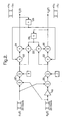
- the demodulator comprises an optical splitter 28 for splitting the received DQPSK modulated optical signal 14 into two parts which are applied to a respective unbalanced Mach-Zehnder interferometer (MZI) 30, 32.
- MZI Mach-Zehnder interferometer
- the MZIs are fabricated in gallium arsenide or lithium niobate.
- a respective balanced optical to electrical converter 34, 36 is connected across the optical outputs of each MZI 30, 32.
- Each MZI 30, 32 is unbalanced in that each has a time delay ⁇ , nominally equal to the symbol period (50 ps for a 20 Gsymbol/s line rate) of the data modulation rate, in one arm 30a, 32a relative to that of the other arm 30b, 32b.
- the time delay ⁇ is introduced by making the optical path length of the two arms different and for ease of fabrication is introduced by making the physical length of the MZI's arm 30a, 32a longer than the other arm 30b, 32b.
- Each MZI 30, 32 is respectively set to impart a relative phase shift of p/4 and -p/4 by the application of an appropriate voltage to electrodes on the shorter arm 30b, 32b.
- a particular benefit of setting the MZIs 30, 32 to impart relative phase shifts between their arms of p/4 and -p/4 respectively is that this results in the de-modulated signals x 1 (t), y 2 (t) being symmetrical bipolar NRZ signals.
- the in-phase and quadrature components of the DQPSK signal can also be demodulated using other relative phase shifts provided there is a difference of p/2 between the respective MZIs ; though the resulting signals will not be symmetrical bipolar NRZ signals.
- the MZI 30 is set to impart a phase shift f and the MZI 32 set to impart a phase shift f ⁇ p/2.
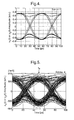
- FIG. 4 there is shown a simulated "eye" diagram for one of the demodulated electrical signals x 1 ( t ) or y 2 ( t ) for a 20Gbit/s data stream for a communications system incorporating the DQPSK modulator and demodulator arrangement of the Figures 1 and 3 .
- Figure 5 shows a further simulated "eye” diagram for the same system for transmission over a 600km optically amplified, dispersion managed optical fibre link and further includes Signal-ASE (Amplitude Spontaneous Emission) noise.
- Signal-ASE Amplitude Spontaneous Emission
- a particular advantage of the signalling format of the present invention is its improved spectral efficiency. Simulations of a DWDM optical link comprising 40 Gbit/s channels with a 50 GHz spacing (0.8 bit/s/Hz spectral efficiency) indicate that such a system is quite viable without requiring polarisation multiplexing/interleaving.
- DQPSK offers a number of advantages compared to other signalling formats such as binary amplitude and binary phase shift signalling.
- Optical DQPSK provides a higher tolerance to chromatic dispersion and a higher tolerance to polarisation mode dispersion.
- a further advantage is that the electrical and optoelectronic components operate with a bandwidth commensurate with half the line bit rate.
- optical DQPSK provides improved tolerance to cross-phase modulation (XPM) since the signal is differentially encoded as a phase difference (change) between successive data bits whilst XPM will in general be common to successive data bits.
- XPM cross-phase modulation
- optical DQPSK does not require a phase-coherent local oscillator for demodulation this eliminates the need for adaptive polarisation control. Since modulation and demodulation for optical DQPSK is functionally relatively straightforward it can readily be implemented using robust and compact electro-optic compact circuits such as phase modulators, optical couplers, splitters etc which can be readily integrated in the form of monolithic waveguide devices.
- optical DQPSK is a viable signalling format for transmission of multiple 40Gb/s DWDM communication channels with tera bit/s capacity over a single optical fibre. It is also envisaged that combined with Raman amplification and forward error correction (FEC), optical DQPSK signalling offers the potential for tera bit/s transmission over several thousands of kilometres of optical fibre.
- FEC forward error correction
- One of the limiting factors for improving spectral efficiency in WDM systems is that tight optical filtering of the modulated wavelength channels before multiplexing using known optical filters (Butterworth) causes inter-symbol interference (ISI) thereby degrading system performance.
- ISI inter-symbol interference
- the inventor has appreciated that the system performance can be further improved by using optical filtering if its characteristic is carefully selected such as to minimise ISI at the sampling times t s for the data symbols.
- the optical spectrum is close to an ideal "sinc" (sin x/x) function and consequently the side lobes are quite high compared to other signalling formats.
- the filter is selected to have an excess bandwidth factor of 0.2 to 0.8.
- the optical nyquist filtering function is split between optical Nyquist filters located at the transmitter and receiver.
- the transmitter optical filter is preferably connected to the output of the modulator arrangement such that each wavelength channel is filtered before multiplexing the channels and the receiver optical filter located after de-multiplexing of the WDM optical signal and before demodulation of the DQPSK signal.
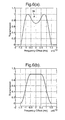
- the optical characteristics of the transmitter and receiver Nyquist filters are illustrated in Figures 6(a) and 6(b) .
- the receiver Nyquist filter characteristic comprises a squared raised cosine function, as defined by Eq.
- the transmitter filter characteristic, Figure 6(a) also essentially comprises a squared raised-cosine function but is further modified in the bandpass region 38 to have a 1/ "sinc" function to take account of the finite pulse width of the transmitted symbols.
- the transmitter and receiver Nyquists are fabricated in the form of optical fibre Bragg gratings or a grating structure defined within an optical waveguide.
Landscapes
- Engineering & Computer Science (AREA)
- Computer Networks & Wireless Communication (AREA)
- Signal Processing (AREA)
- Power Engineering (AREA)
- Physics & Mathematics (AREA)
- Electromagnetism (AREA)
- Optical Communication System (AREA)
- Optical Modulation, Optical Deflection, Nonlinear Optics, Optical Demodulation, Optical Logic Elements (AREA)
Applications Claiming Priority (2)
| Application Number | Priority Date | Filing Date | Title |
|---|---|---|---|
| GB0031386A GB2370473B (en) | 2000-12-21 | 2000-12-21 | Improvements in or relating to optical communication |
| EP01271709A EP1344362A2 (de) | 2000-12-21 | 2001-12-18 | Wdm-kommunikationssystem unter verwendung von dmpsk und optischer filterung |
Related Parent Applications (2)
| Application Number | Title | Priority Date | Filing Date |
|---|---|---|---|
| EP01271709.6 Division | 2001-12-18 | ||
| EP01271709A Division EP1344362A2 (de) | 2000-12-21 | 2001-12-18 | Wdm-kommunikationssystem unter verwendung von dmpsk und optischer filterung |
Publications (3)
| Publication Number | Publication Date |
|---|---|
| EP2278763A2 true EP2278763A2 (de) | 2011-01-26 |
| EP2278763A3 EP2278763A3 (de) | 2012-09-26 |
| EP2278763B1 EP2278763B1 (de) | 2016-05-11 |
Family
ID=9905690
Family Applications (3)
| Application Number | Title | Priority Date | Filing Date |
|---|---|---|---|
| EP01271709A Withdrawn EP1344362A2 (de) | 2000-12-21 | 2001-12-18 | Wdm-kommunikationssystem unter verwendung von dmpsk und optischer filterung |
| EP10011560.9A Expired - Lifetime EP2278762B1 (de) | 2000-12-21 | 2001-12-18 | Vorrichtung und verfahren zur optischen modulation |
| EP10012232.4A Expired - Lifetime EP2278763B1 (de) | 2000-12-21 | 2001-12-18 | Optischer Demodulator |
Family Applications Before (2)
| Application Number | Title | Priority Date | Filing Date |
|---|---|---|---|
| EP01271709A Withdrawn EP1344362A2 (de) | 2000-12-21 | 2001-12-18 | Wdm-kommunikationssystem unter verwendung von dmpsk und optischer filterung |
| EP10011560.9A Expired - Lifetime EP2278762B1 (de) | 2000-12-21 | 2001-12-18 | Vorrichtung und verfahren zur optischen modulation |
Country Status (8)
| Country | Link |
|---|---|
| US (3) | US7546041B2 (de) |
| EP (3) | EP1344362A2 (de) |
| JP (3) | JP4558271B2 (de) |
| CN (1) | CN100481824C (de) |
| AU (1) | AU2002222266A1 (de) |
| CA (1) | CA2432007A1 (de) |
| GB (1) | GB2370473B (de) |
| WO (1) | WO2002051041A2 (de) |
Families Citing this family (153)
| Publication number | Priority date | Publication date | Assignee | Title |
|---|---|---|---|---|
| US20030007216A1 (en) * | 2001-06-21 | 2003-01-09 | Chraplyvy Andrew Roman | Long haul transmission in a dispersion managed optical communication system |
| GB2383707B (en) * | 2001-11-30 | 2005-03-30 | Marconi Optical Components Ltd | Photonic encoder |
| GB2383705B (en) | 2001-11-30 | 2005-03-30 | Marconi Optical Components Ltd | Optical coding system |
| GB2383706B (en) * | 2001-11-30 | 2005-03-30 | Marconi Optical Components Ltd | Modulation control |
| US20040208646A1 (en) * | 2002-01-18 | 2004-10-21 | Seemant Choudhary | System and method for multi-level phase modulated communication |
| GB2385144B (en) * | 2002-01-23 | 2006-02-08 | Marconi Optical Components Ltd | Optical signal demodulators |
| US7277645B2 (en) * | 2002-03-14 | 2007-10-02 | Lucent Technologies Inc. | High-bit-rate long-haul fiber optic communication system techniques and arrangements |
| JP4047099B2 (ja) * | 2002-08-20 | 2008-02-13 | 富士通株式会社 | 時分割多重信号光の分離装置、並びに、それを用いた光受信装置および光伝送システム |
| US7382984B2 (en) | 2002-10-03 | 2008-06-03 | Nortel Networks Limited | Electrical domain compensation of optical dispersion in an optical communications system |
| EP1411658A3 (de) * | 2002-10-15 | 2005-08-03 | Alcatel | Optischer MSK Sender |
| US7190908B2 (en) * | 2002-10-28 | 2007-03-13 | The Boeing Company | Optical differential quadrature phase-shift keyed decoder |
| US8050351B2 (en) * | 2003-07-02 | 2011-11-01 | Celight, Inc. | Quadrature modulator with feedback control and optical communications system using the same |
| JP3829198B2 (ja) * | 2003-12-01 | 2006-10-04 | 独立行政法人情報通信研究機構 | 光伝送方法及びシステム |
| DE102004021816A1 (de) * | 2004-04-30 | 2005-11-24 | Universität Stuttgart | Gerät und Methode zur optischen achtstufigen differentiellen Phasenumtastung (8-DPSK) |
| US7317845B2 (en) * | 2004-06-23 | 2008-01-08 | Lucent Technologies Inc. | Optical modulator having reduced bandwidth requirements and method of operation thereof |
| US7433604B1 (en) * | 2004-07-21 | 2008-10-07 | University Of Central Florida Research Foundation, Inc. | Direct-detection optical differential 8-level phase shift keying (OD8PSK) for spectrally efficient transmission |
| JP2006039037A (ja) * | 2004-07-23 | 2006-02-09 | Mitsubishi Electric Corp | 半導体光遅延干渉器 |
| JP3920297B2 (ja) * | 2004-09-01 | 2007-05-30 | 富士通株式会社 | 光スイッチおよび光スイッチを利用した光波形モニタ装置 |
| DE102004047028A1 (de) * | 2004-09-28 | 2006-04-20 | Siemens Ag | Verfahren und Anordnung zur optischen Übertragung von Datensignalen mittels differentieller Phasenmodulation in einem Polarisations-Multiplexverfahren |
| US7676161B2 (en) * | 2004-12-10 | 2010-03-09 | Nortel Networks Limited | Modulation E-field based control of a non-linear transmitter |
| JP4170298B2 (ja) * | 2005-01-31 | 2008-10-22 | 富士通株式会社 | 差分4位相偏移変調方式に対応した光受信器および光受信方法 |
| JP4675796B2 (ja) * | 2005-02-15 | 2011-04-27 | 日本電信電話株式会社 | 自動分散補償型光伝送システム |
| JP2006245647A (ja) * | 2005-02-28 | 2006-09-14 | Fujitsu Ltd | 差動位相偏移変調方式に対応した送信器及びトランスポンダ |
| JP4589836B2 (ja) * | 2005-02-28 | 2010-12-01 | 富士通株式会社 | 光信号受信装置 |
| JP4727493B2 (ja) * | 2006-04-20 | 2011-07-20 | 富士通株式会社 | 光信号受信装置及び光信号受信制御方法 |
| US7689133B2 (en) * | 2005-02-28 | 2010-03-30 | Fujitsu Limited | Optical signal reception device and method of controlling optical signal reception |
| US7389055B1 (en) | 2005-03-17 | 2008-06-17 | Nortel Networks Limited | DQPSK receiver phase control |
| JP4561443B2 (ja) * | 2005-03-31 | 2010-10-13 | 富士通株式会社 | M相差分位相偏移変調方式に対応した光受信器 |
| JP4710387B2 (ja) * | 2005-04-06 | 2011-06-29 | 富士通株式会社 | 差分m位相偏移変調方式に対応した光受信器および光受信方法 |
| JP4602148B2 (ja) * | 2005-04-12 | 2010-12-22 | 三菱電機株式会社 | 光受信器 |
| JP4922594B2 (ja) | 2005-05-23 | 2012-04-25 | 富士通株式会社 | 光送信装置、光受信装置、およびそれらを含む光通信システム |
| US20060263097A1 (en) * | 2005-05-23 | 2006-11-23 | Fujitsu Limited | Optical transmitting apparatus, optical receiving apparatus, and optical communication system comprising them |
| JP4466861B2 (ja) | 2005-06-27 | 2010-05-26 | 横河電機株式会社 | Qpsk光変調装置 |
| CN1893324A (zh) * | 2005-07-08 | 2007-01-10 | 富士通株式会社 | 光dqpsk接收机的相位监测装置、相位控制装置及其方法 |
| KR100640509B1 (ko) * | 2005-08-01 | 2006-10-30 | 삼성전자주식회사 | 단측파대 변조 모듈 |
| JP4516501B2 (ja) * | 2005-08-25 | 2010-08-04 | 富士通オプティカルコンポーネンツ株式会社 | Dqpsk光受信回路 |
| JP4440855B2 (ja) * | 2005-08-25 | 2010-03-24 | 富士通株式会社 | Rz−dpsk光受信回路 |
| JP4516907B2 (ja) * | 2005-08-26 | 2010-08-04 | 富士通株式会社 | 光受信装置およびその制御方法 |
| JP4437985B2 (ja) * | 2005-08-31 | 2010-03-24 | 富士通株式会社 | 多値差動光信号受信器 |
| JP4422661B2 (ja) | 2005-08-31 | 2010-02-24 | 富士通株式会社 | 差動4位相偏移変調器の駆動電圧設定方法 |
| JP4657860B2 (ja) | 2005-09-16 | 2011-03-23 | 富士通株式会社 | 光送信装置および光通信システム |
| JP4440864B2 (ja) | 2005-09-26 | 2010-03-24 | 富士通株式会社 | 光受信装置 |
| US8320779B2 (en) * | 2005-10-05 | 2012-11-27 | Nec Corporation | Light receiver, optical communication system and method |
| US7526210B2 (en) * | 2005-10-08 | 2009-04-28 | Alcatel-Lucent Usa Inc. | Optical demodulating apparatus and method |
| JP4752469B2 (ja) * | 2005-11-30 | 2011-08-17 | 横河電機株式会社 | 復調器 |
| JP4781094B2 (ja) | 2005-11-30 | 2011-09-28 | 富士通株式会社 | 光送信装置 |
| JP4695500B2 (ja) * | 2005-12-02 | 2011-06-08 | 富士通株式会社 | 信号再生装置,光受信装置および信号処理方法 |
| JP4768421B2 (ja) * | 2005-12-06 | 2011-09-07 | 富士通株式会社 | Dqpsk光受信器 |
| JP4767676B2 (ja) * | 2005-12-12 | 2011-09-07 | 三菱電機株式会社 | 光受信装置 |
| US20070206898A1 (en) * | 2006-01-03 | 2007-09-06 | Nec Laboratories America | Optical equalization filtering of dwdm channels |
| JP4695989B2 (ja) | 2006-01-27 | 2011-06-08 | 富士通株式会社 | 差動m位相偏移変調信号の復調用干渉計 |
| JP4563944B2 (ja) * | 2006-01-31 | 2010-10-20 | 富士通株式会社 | 光送信器 |
| JP4755205B2 (ja) | 2006-02-03 | 2011-08-24 | 富士通株式会社 | 光変調器の駆動回路 |
| US7623796B2 (en) * | 2006-02-27 | 2009-11-24 | Alcatel-Lucent Usa Inc. | Data-aided multi-symbol phase estimation for optical differential multilevel phase-shift keying signals |
| JP2007240389A (ja) | 2006-03-09 | 2007-09-20 | Fujitsu Ltd | 光波形測定装置および光波形測定方法 |
| CN101043269B (zh) * | 2006-03-22 | 2011-01-05 | 富士通株式会社 | I-q正交调制发射机及其i-q路间相位偏置的监测装置和方法 |
| JP4708241B2 (ja) * | 2006-03-28 | 2011-06-22 | 三菱電機株式会社 | 分散予等化光送信器 |
| JP2007274235A (ja) * | 2006-03-30 | 2007-10-18 | Fujitsu Ltd | 光dqpsk受信器 |
| EP2003486A4 (de) * | 2006-03-31 | 2010-11-24 | Fujitsu Ltd | Differenz-vierphasen-verschiebungs-modulator und verfahren zum steuern des phasenverschiebungsbetrags dafür |
| JP4678653B2 (ja) * | 2006-05-09 | 2011-04-27 | 富士通株式会社 | 光送信装置 |
| JP4655996B2 (ja) | 2006-05-12 | 2011-03-23 | 横河電機株式会社 | 遅延干渉計及び復調器 |
| JP4531010B2 (ja) * | 2006-05-26 | 2010-08-25 | 日本電信電話株式会社 | 光位相変復調回路および光位相変復調方法 |
| JP4915147B2 (ja) * | 2006-06-15 | 2012-04-11 | 富士通株式会社 | 位相制御装置および光dqpsk受信機 |
| JP2008010971A (ja) | 2006-06-27 | 2008-01-17 | Fujitsu Ltd | 高速分散補償制御装置 |
| US7650083B2 (en) * | 2006-06-30 | 2010-01-19 | Fujitsu Limited | Demodulating a signal by performing consecutive beam splitting |
| JP4684180B2 (ja) | 2006-06-30 | 2011-05-18 | 富士通株式会社 | 光受信装置 |
| JP5040203B2 (ja) | 2006-07-19 | 2012-10-03 | 富士通株式会社 | 光信号受信装置および光信号受信制御方法 |
| JP4620642B2 (ja) * | 2006-07-31 | 2011-01-26 | 富士通株式会社 | 多値変調受信装置 |
| US20090016739A1 (en) * | 2006-07-31 | 2009-01-15 | Nec Laboratories America | Pattern effect reduction of optical signals |
| JP4983178B2 (ja) * | 2006-09-15 | 2012-07-25 | 富士通株式会社 | 差動四位相偏移変調光受信回路 |
| JP4783702B2 (ja) | 2006-09-15 | 2011-09-28 | 富士通株式会社 | 光受信装置 |
| US9312964B2 (en) * | 2006-09-22 | 2016-04-12 | Alcatel Lucent | Reconstruction and restoration of an optical signal field |
| JP5405716B2 (ja) | 2006-09-29 | 2014-02-05 | 富士通株式会社 | 光送信機 |
| JP2008099178A (ja) * | 2006-10-16 | 2008-04-24 | Nippon Telegr & Teleph Corp <Ntt> | 多値光位相変調回路および多値光位相変調伝送システム |
| JP5055947B2 (ja) * | 2006-10-20 | 2012-10-24 | 富士通オプティカルコンポーネンツ株式会社 | 光変調器および送信装置 |
| JP5055968B2 (ja) * | 2006-11-14 | 2012-10-24 | 富士通株式会社 | 差動4位相偏移変調器 |
| JP4842100B2 (ja) * | 2006-11-14 | 2011-12-21 | 三菱電機株式会社 | 分散予等化光送信器および光通信システム |
| US9230695B2 (en) | 2006-11-28 | 2016-01-05 | Terrapower, Llc | Nuclear fission igniter |
| US9214246B2 (en) | 2006-11-28 | 2015-12-15 | Terrapower, Llc | System and method for operating a modular nuclear fission deflagration wave reactor |
| US9734922B2 (en) | 2006-11-28 | 2017-08-15 | Terrapower, Llc | System and method for operating a modular nuclear fission deflagration wave reactor |
| JP2008141670A (ja) * | 2006-12-05 | 2008-06-19 | Fujitsu Ltd | Dqpsk変調装置、光送信装置およびdqpsk変調方法 |
| JP5233115B2 (ja) * | 2006-12-22 | 2013-07-10 | 日本電気株式会社 | Dqpsk復調方法を用いた光受信装置およびdqpsk復調方法 |
| JP4522417B2 (ja) * | 2007-01-15 | 2010-08-11 | 富士通株式会社 | 光変調装置および光変調方法 |
| JP4770741B2 (ja) * | 2007-01-17 | 2011-09-14 | 日本電気株式会社 | 光伝送システム及びその方法並びにそれに用いる光送受信装置 |
| JP2008187223A (ja) * | 2007-01-26 | 2008-08-14 | Hitachi Communication Technologies Ltd | 光位相変調器の制御法 |
| JP4818142B2 (ja) | 2007-02-06 | 2011-11-16 | 富士通株式会社 | 光受信装置およびその制御方法、並びに、光伝送システム |
| JP2008224313A (ja) | 2007-03-09 | 2008-09-25 | Yokogawa Electric Corp | 干渉計及び復調器 |
| US8503889B2 (en) | 2007-03-23 | 2013-08-06 | Massachusetts Institute Of Technology | Filter-based DPSK receiver |
| JP5168973B2 (ja) | 2007-03-27 | 2013-03-27 | 横河電機株式会社 | 干渉計及び復調器並びに分岐素子 |
| US20080240736A1 (en) * | 2007-03-28 | 2008-10-02 | Nec Laboratories America, Inc. | Inter-Symbol Interference-Suppressed Colorless DPSK Demodulation |
| JP5092827B2 (ja) | 2007-03-29 | 2012-12-05 | 富士通株式会社 | 光dqpsk受信器及び、異常検出制御方法 |
| US20090214224A1 (en) * | 2007-04-03 | 2009-08-27 | Celight, Inc. | Method and apparatus for coherent analog rf photonic transmission |
| JP4983466B2 (ja) * | 2007-07-30 | 2012-07-25 | 富士通株式会社 | 光変調装置および光変調方法ならびに光送信装置 |
| WO2009023302A2 (en) * | 2007-08-14 | 2009-02-19 | Rambus Inc. | Communication using continuous-phase modulated signals |
| JP4934557B2 (ja) * | 2007-09-27 | 2012-05-16 | 株式会社日立製作所 | 4値位相変調器 |
| EP2209038B1 (de) * | 2007-10-10 | 2014-06-25 | NEC Corporation | Optischer modulator und optisches kommunikationssystem |
| JP5550825B2 (ja) * | 2007-10-16 | 2014-07-16 | ジェイディーエス ユニフェイズ コーポレーション | モニタリング構造を備えた光位相変調器 |
| JP5061855B2 (ja) | 2007-11-07 | 2012-10-31 | 富士通株式会社 | 電気分散補償装置、光受信装置および光受信方法 |
| JP5012457B2 (ja) | 2007-11-30 | 2012-08-29 | 富士通株式会社 | Dqpsk光受信装置 |
| JP4973476B2 (ja) | 2007-12-10 | 2012-07-11 | Kddi株式会社 | 光信号品質監視装置 |
| MX2007016078A (es) * | 2007-12-14 | 2009-06-15 | Itesm | Modulador y demodulador para un formato de modulación óptico diferencial con ocho cambios de fase. |
| US8064768B2 (en) * | 2007-12-19 | 2011-11-22 | Nec Laboratories America, Inc. | Intra-channel equalizing optical interleaver |
| US8472812B2 (en) | 2008-02-22 | 2013-06-25 | Nec Corporation | Optical communication system, optical communication method and optical communication apparatus |
| JP2009200915A (ja) * | 2008-02-22 | 2009-09-03 | Fujitsu Ltd | 光dqpsk受信機、および光dqpsk受信機において使用される光位相モニタ装置 |
| JP5088174B2 (ja) * | 2008-02-28 | 2012-12-05 | 富士通株式会社 | 復調回路 |
| JP5487547B2 (ja) * | 2008-02-28 | 2014-05-07 | 富士通株式会社 | 光変調装置および光変調方法 |
| JP2009232330A (ja) * | 2008-03-25 | 2009-10-08 | Yokogawa Electric Corp | 光受信機 |
| US20090252502A1 (en) * | 2008-04-07 | 2009-10-08 | Futurewei Technologies, Inc. | Methods and systems for optical communication |
| JP5038219B2 (ja) * | 2008-04-11 | 2012-10-03 | 株式会社日立製作所 | 光受信装置 |
| US7962043B2 (en) * | 2008-06-20 | 2011-06-14 | Applied Micro Circuits Corporation | Multichannel optical transport network skew control |
| CN101621336B (zh) * | 2008-06-30 | 2012-12-12 | 华为技术有限公司 | 一种差分正交相移键控系统、方法及设备 |
| WO2010050124A1 (ja) * | 2008-10-31 | 2010-05-06 | 株式会社日立製作所 | 光受信機 |
| JP2010130323A (ja) * | 2008-11-27 | 2010-06-10 | Yokogawa Electric Corp | 光伝送装置 |
| JP5264521B2 (ja) | 2009-01-16 | 2013-08-14 | 三菱電機株式会社 | 光送信器 |
| JP2010245905A (ja) * | 2009-04-07 | 2010-10-28 | Sony Corp | 送信装置および通信システム |
| US8213810B2 (en) * | 2009-06-22 | 2012-07-03 | Agilent Technologies, Inc. | Demodulation of an optical signal under control of a kalman filter |
| JP2011022479A (ja) | 2009-07-17 | 2011-02-03 | Mitsubishi Electric Corp | 多値光送信器 |
| US9020361B2 (en) * | 2009-09-08 | 2015-04-28 | Nippon Telegraph And Telephone Corporation | Optical signal transmitter, and bias voltage control method |
| WO2011045674A1 (en) | 2009-10-16 | 2011-04-21 | Oclaro Technology Limited | Method and system for deploying an optical demodulator arrangement in a communications network |
| WO2011084035A2 (en) * | 2010-01-11 | 2011-07-14 | Samsung Electronics Co., Ltd. | Ultra-wide band communication apparatus and method |
| JP5421792B2 (ja) * | 2010-01-12 | 2014-02-19 | 株式会社日立製作所 | 偏波多重送信器及び伝送システム |
| JP5351788B2 (ja) | 2010-01-29 | 2013-11-27 | 富士通テレコムネットワークス株式会社 | 光受信装置および光伝送システム |
| JP5482351B2 (ja) | 2010-03-19 | 2014-05-07 | 富士通株式会社 | 光変調装置及び光変調方法 |
| JP5263205B2 (ja) | 2010-03-19 | 2013-08-14 | 富士通株式会社 | 光変調装置及び光変調方法 |
| JP5015284B2 (ja) * | 2010-03-30 | 2012-08-29 | 株式会社日立製作所 | 光送信器、光送信方法、及び、光送受信システム |
| CN103168437B (zh) | 2010-05-20 | 2016-04-27 | 奥兰若有限公司 | 无需fec反馈的自适应接收器 |
| US8483574B2 (en) * | 2010-10-15 | 2013-07-09 | Tyco Electronics Subsea Communications, Llc | Correlation-control QPSK transmitter |
| GB2485202B (en) | 2010-11-05 | 2017-08-30 | Oclaro Tech Ltd | Demodulator and optical arrangement thereof |
| WO2012088669A1 (zh) * | 2010-12-29 | 2012-07-05 | 昂纳信息技术(深圳)有限公司 | 一种mems芯片调节相位的解调器 |
| JP5006978B1 (ja) | 2011-03-30 | 2012-08-22 | 株式会社フジクラ | 補償方法、光変調システム、及び光復調システム |
| WO2011107055A2 (zh) * | 2011-04-20 | 2011-09-09 | 华为技术有限公司 | 基于微波光子技术的信号接收装置和信号接收方法 |
| WO2012157182A1 (ja) | 2011-05-13 | 2012-11-22 | 日本電気株式会社 | 信号同期送信システム、光変調器用同期駆動システム、信号同期送信方法及びそのプログラムが格納された非一時的なコンピュータ可読媒体 |
| US8606114B2 (en) | 2011-05-17 | 2013-12-10 | Oclaro Technology Limited | Alignment of a data signal to an alignment signal |
| CN102420661B (zh) * | 2011-12-15 | 2014-06-04 | 华中科技大学 | 一种光纤非线性损伤补偿装置 |
| JP2013183455A (ja) * | 2012-02-29 | 2013-09-12 | Zte (Usa) Inc | ナイキスト波長分割多重システム |
| US8515865B1 (en) * | 2012-05-26 | 2013-08-20 | At&T Intellectual Property I, L.P. | Methods, systems, and products for charging batteries |
| EP2688232B1 (de) | 2012-07-19 | 2017-06-14 | Alcatel Lucent | Optischer Sender zum Senden eines mehrstufigen amplitudentastungsmodulierten Signals |
| WO2014025683A2 (en) | 2012-08-06 | 2014-02-13 | Skorpios Technologies, Inc. | Method and system for the monolithic integration of circuits for monitoring and control of rf signals |
| US9270379B2 (en) * | 2013-03-18 | 2016-02-23 | Nec Laboratories America, Inc. | Optical nyquist superchannel generation using microwave low-pass filtering and optical equalization |
| WO2015027903A1 (en) * | 2013-08-27 | 2015-03-05 | Zte Corporation | Optical communication using super-nyquist signals |
| JP6446803B2 (ja) * | 2014-03-25 | 2019-01-09 | 日本電気株式会社 | 光送受信器 |
| US9838239B2 (en) * | 2015-01-22 | 2017-12-05 | Futurewei Technologies, Inc. | Digital generation of multi-level phase shifting with a Mach-Zehnder modulator (MZM) |
| JP6620409B2 (ja) * | 2015-03-11 | 2019-12-18 | 富士通株式会社 | 光送信器、光伝送システム、及び光通信制御方法 |
| CN106128406B (zh) * | 2016-09-08 | 2019-01-22 | 京东方科技集团股份有限公司 | 眼图幅值调节方法、数据传输方法、电路和显示装置 |
| US10673530B2 (en) * | 2016-10-05 | 2020-06-02 | LGS Innovations LLC Inc. | Free space optical communication system and method |
| ES2810723T3 (es) | 2016-10-08 | 2021-03-09 | Huawei Tech Co Ltd | Procedimiento y dispositivo de ecualización de potencia óptica |
| CN107346991B (zh) * | 2017-06-22 | 2019-10-29 | 北京工业大学 | 一种基于相位敏感放大的多路mpsk信号再生方法 |
| US10749600B2 (en) * | 2018-04-12 | 2020-08-18 | The Boeing Company | Systems and methods for single optical fiber data transmission |
| AT521851A1 (de) * | 2018-11-13 | 2020-05-15 | Ait Austrian Inst Tech Gmbh | Verfahren zur Übertragung von Daten und/oder Informationen |
| WO2020207691A1 (en) * | 2019-04-12 | 2020-10-15 | Telefonaktiebolaget Lm Ericsson (Publ) | Encoding and decoding communications traffic in a pulse amplitude modulation format and optical apparatus for same |
| JP2022150173A (ja) * | 2021-03-26 | 2022-10-07 | 富士通株式会社 | 光送信器及び伝送装置 |
| US20230281437A1 (en) * | 2022-03-01 | 2023-09-07 | Massachusetts Institute Of Technology | Radio-Frequency Photonic Architecture for Deep Neural Networks, Signal Processing, and Computing |
| KR102723528B1 (ko) * | 2023-03-02 | 2024-10-29 | 국방과학연구소 | 자유공간 광통신 장치 및 방법 |
Family Cites Families (45)
| Publication number | Priority date | Publication date | Assignee | Title |
|---|---|---|---|---|
| US137604A (en) * | 1873-04-08 | Samuel s | ||
| JPS631220A (ja) | 1986-06-20 | 1988-01-06 | Toshiba Corp | ロ−ルオフフイルタ |
| JPS6352530A (ja) * | 1986-08-22 | 1988-03-05 | Fujitsu Ltd | コヒ−レント光通信用の受信器 |
| JPS6386608A (ja) | 1986-09-30 | 1988-04-18 | Toshiba Corp | ロ−ルオフフイルタ |
| JPH069336Y2 (ja) | 1987-06-26 | 1994-03-09 | 株式会社島津製作所 | 電子天びん |
| JPS645127A (en) * | 1987-06-29 | 1989-01-10 | Nec Corp | Optical transmitter |
| US4933929A (en) | 1987-06-29 | 1990-06-12 | Nec Corporation | Wavelength multiplexed optical transmitter for generating constant-amplitude angle-modulated beams to eliminate phase noise in adjacent transmission channels |
| JPS647727A (en) * | 1987-06-30 | 1989-01-11 | Nec Corp | Light transmission equipment |
| US4893352A (en) * | 1987-06-30 | 1990-01-09 | Massachusetts Institute Of Technology | Optical transmitter of modulated signals |
| JPS647727U (de) | 1987-07-04 | 1989-01-17 | ||
| IT1232056B (it) * | 1989-03-28 | 1992-01-23 | Cselt Centro Studi Lab Telecom | Modulatore veloce della polarizza zione di una portante ottica |
| JP2758211B2 (ja) * | 1989-06-19 | 1998-05-28 | 富士通株式会社 | 周波数直接変調psk方式 |
| JP2760856B2 (ja) | 1989-08-18 | 1998-06-04 | 富士通株式会社 | マッハツェンダ型光変調器を用いた位相シフトキーイング方式 |
| EP0431527B1 (de) | 1989-12-04 | 1995-03-15 | Canon Kabushiki Kaisha | Optisches Kopplergerät mit wellenlängeselektivem optischem Koppler |
| JP2836050B2 (ja) | 1989-12-04 | 1998-12-14 | キヤノン株式会社 | 光波長フィルター及びそれを用いた装置 |
| JPH03179939A (ja) | 1989-12-08 | 1991-08-05 | Fujitsu Ltd | 多相位相変調器 |
| JPH03259632A (ja) | 1990-03-09 | 1991-11-19 | Fujitsu Ltd | 光ヘテロダイン偏波ダイバーシティ受信器 |
| JPH0478235A (ja) * | 1990-07-18 | 1992-03-12 | Fujitsu Ltd | 直接変調psk伝送システム並びに該システムにおける自動周波数制御方法、復調方法及び位相雑音抑圧方法 |
| EP0477699A3 (en) * | 1990-09-14 | 1993-09-01 | Fujitsu Limited | Optical communication system |
| US5222103A (en) * | 1991-01-02 | 1993-06-22 | Gte Laboratories Incorporated | Differential quadrature phase shift keying encoder for subcarrier systems |
| US5101450A (en) * | 1991-01-23 | 1992-03-31 | Gte Laboratories Incorporated | Quadrature optical phase modulators for lightwave systems |
| JP3053966B2 (ja) | 1992-06-01 | 2000-06-19 | キヤノン株式会社 | 方向性結合器フィルタ |
| JPH06224852A (ja) * | 1993-01-25 | 1994-08-12 | Matsushita Electric Ind Co Ltd | 光伝送方式 |
| JP3179939B2 (ja) | 1993-06-16 | 2001-06-25 | ミサワホーム株式会社 | 化粧石膏ボードの幅詰め方法および化粧石膏ボード |
| JP3259632B2 (ja) | 1995-05-31 | 2002-02-25 | カシオ計算機株式会社 | 反強誘電性液晶表示素子 |
| JPH09214429A (ja) | 1996-02-05 | 1997-08-15 | Kokusai Denshin Denwa Co Ltd <Kdd> | 光アクセス方式 |
| JP3174503B2 (ja) | 1996-04-01 | 2001-06-11 | 新日本製鐵株式会社 | プレス加工性の優れた表面処理鋼板の製造方法 |
| KR100239169B1 (ko) * | 1996-04-04 | 2000-01-15 | 윤종용 | 파이/n 쉬프티트 n차분위상쉬프트키잉 변조신호 발생장치 |
| JP3430454B2 (ja) | 1996-06-27 | 2003-07-28 | 日本電信電話株式会社 | 光波長分割多重伝送装置 |
| JP3297325B2 (ja) | 1996-11-13 | 2002-07-02 | 株式会社東芝 | 光通信装置 |
| US6137604A (en) | 1996-12-04 | 2000-10-24 | Tyco Submarine Systems, Ltd. | Chromatic dispersion compensation in wavelength division multiplexed optical transmission systems |
| JP3094950B2 (ja) * | 1997-05-28 | 2000-10-03 | 日本電気株式会社 | 光送信装置及び光送信方法 |
| JP4184474B2 (ja) | 1997-08-22 | 2008-11-19 | 松下電器産業株式会社 | 光伝送システムならびにそれに用いられる光送信装置および光受信装置 |
| JPH11220443A (ja) * | 1998-01-30 | 1999-08-10 | Nippon Telegr & Teleph Corp <Ntt> | 光送受信方式 |
| US6111679A (en) * | 1998-04-21 | 2000-08-29 | Optimight Communications, Inc. | Method and system for optical multichannel transmission using coherence division multiplexing with optical filtering |
| EP0977382B1 (de) | 1998-07-29 | 2009-05-13 | Nippon Telegraph and Telephone Corporation | Optisches Übertragungssystem |
| JP3371857B2 (ja) | 1998-07-29 | 2003-01-27 | 日本電信電話株式会社 | 光伝送装置 |
| JP2000059300A (ja) | 1998-08-06 | 2000-02-25 | Nippon Telegr & Teleph Corp <Ntt> | 光送受信装置 |
| JP2000092001A (ja) | 1998-09-09 | 2000-03-31 | Nippon Telegr & Teleph Corp <Ntt> | 光送信装置 |
| JP2000151505A (ja) * | 1998-11-09 | 2000-05-30 | Nippon Telegr & Teleph Corp <Ntt> | 光送受信装置 |
| JP2000157505A (ja) | 1998-11-30 | 2000-06-13 | Ge Yokogawa Medical Systems Ltd | テーブル及びmri装置 |
| JP2000209162A (ja) | 1999-01-12 | 2000-07-28 | Hitachi Cable Ltd | 光波長多重用光源 |
| US6628728B1 (en) | 1999-04-28 | 2003-09-30 | Cyntrust Communications, Inc. | Nyquist filter and method |
| JP3625726B2 (ja) * | 2000-03-06 | 2005-03-02 | 日本電信電話株式会社 | 光伝送装置および光伝送システム |
| US6697576B1 (en) * | 2000-07-20 | 2004-02-24 | Northrop Grumman Corporation | Wideband, high-fidelity analog optical link design |
-
2000
- 2000-12-21 GB GB0031386A patent/GB2370473B/en not_active Expired - Lifetime
-
2001
- 2001-12-18 EP EP01271709A patent/EP1344362A2/de not_active Withdrawn
- 2001-12-18 US US10/451,464 patent/US7546041B2/en not_active Expired - Lifetime
- 2001-12-18 JP JP2002552220A patent/JP4558271B2/ja not_active Expired - Fee Related
- 2001-12-18 EP EP10011560.9A patent/EP2278762B1/de not_active Expired - Lifetime
- 2001-12-18 AU AU2002222266A patent/AU2002222266A1/en not_active Abandoned
- 2001-12-18 CN CNB018227465A patent/CN100481824C/zh not_active Expired - Lifetime
- 2001-12-18 EP EP10012232.4A patent/EP2278763B1/de not_active Expired - Lifetime
- 2001-12-18 CA CA002432007A patent/CA2432007A1/en not_active Abandoned
- 2001-12-18 WO PCT/GB2001/005624 patent/WO2002051041A2/en not_active Ceased
-
2009
- 2009-06-08 US US12/480,573 patent/US8213806B2/en not_active Expired - Fee Related
-
2010
- 2010-03-15 JP JP2010057453A patent/JP5005786B2/ja not_active Expired - Lifetime
- 2010-03-15 JP JP2010057452A patent/JP5059155B2/ja not_active Expired - Fee Related
- 2010-10-04 US US12/897,172 patent/US8200099B2/en not_active Expired - Fee Related
Non-Patent Citations (2)
| Title |
|---|
| M. ROHDE ET AL.: "Robustness of DPSK direct detection transmission format in standard fibre WDM systems", ELECTRON. LETT., vol. 36, 2000, XP006015582, DOI: doi:10.1049/el:20000981 |
| S. YAMAZAKI; K. EMURA: "Feasibility study on QPSK optical heterodyne detection system", J. LIGHTWAVE TECLINOL., vol. 8, 1990, pages 1646 - 1653, XP000174434, DOI: doi:10.1109/50.60560 |
Also Published As
| Publication number | Publication date |
|---|---|
| US8213806B2 (en) | 2012-07-03 |
| WO2002051041A2 (en) | 2002-06-27 |
| US20110020013A1 (en) | 2011-01-27 |
| JP5005786B2 (ja) | 2012-08-22 |
| GB2370473A (en) | 2002-06-26 |
| CN100481824C (zh) | 2009-04-22 |
| JP2004516743A (ja) | 2004-06-03 |
| US20040081470A1 (en) | 2004-04-29 |
| US20090245814A1 (en) | 2009-10-01 |
| EP2278762A2 (de) | 2011-01-26 |
| JP2010154559A (ja) | 2010-07-08 |
| US7546041B2 (en) | 2009-06-09 |
| JP4558271B2 (ja) | 2010-10-06 |
| EP2278762A3 (de) | 2012-09-26 |
| EP2278763B1 (de) | 2016-05-11 |
| EP2278763A3 (de) | 2012-09-26 |
| GB0031386D0 (en) | 2001-02-07 |
| JP5059155B2 (ja) | 2012-10-24 |
| GB2370473B (en) | 2004-04-07 |
| JP2010136457A (ja) | 2010-06-17 |
| EP1344362A2 (de) | 2003-09-17 |
| WO2002051041A3 (en) | 2002-10-17 |
| EP2278762B1 (de) | 2016-09-28 |
| CN1491510A (zh) | 2004-04-21 |
| US8200099B2 (en) | 2012-06-12 |
| CA2432007A1 (en) | 2002-06-27 |
| AU2002222266A1 (en) | 2002-07-01 |
Similar Documents
| Publication | Publication Date | Title |
|---|---|---|
| EP2278762B1 (de) | Vorrichtung und verfahren zur optischen modulation | |
| US7327961B2 (en) | Differential encoder for an optical DQPSK modulator | |
| US7116460B2 (en) | Modulation control | |
| JP4278332B2 (ja) | 光送信器および光伝送システム | |
| US7035486B2 (en) | Photonic integrated device | |
| US7398022B2 (en) | Optical return-to-zero phase-shift keying with improved transmitters | |
| US7277647B2 (en) | System and method of optical transmission | |
| US7349636B2 (en) | Optical phase and intensity modulation with improved transmitters | |
| US7925169B2 (en) | Photonic encoder | |
| US8687970B2 (en) | Modulator and demodulator for a differential optical modulation format with eight phase changes | |
| US20060013596A1 (en) | Bandwidth limited frequency shift keying modulation format | |
| US20080199189A1 (en) | Colorless optical demodulator for differential quadrature phase shift keying dwdm systems | |
| US8280261B2 (en) | Optical signal phase regenerator for formats of differential modulation with phase changes |
Legal Events
| Date | Code | Title | Description |
|---|---|---|---|
| PUAI | Public reference made under article 153(3) epc to a published international application that has entered the european phase |
Free format text: ORIGINAL CODE: 0009012 |
|
| AC | Divisional application: reference to earlier application |
Ref document number: 1344362 Country of ref document: EP Kind code of ref document: P |
|
| AK | Designated contracting states |
Kind code of ref document: A2 Designated state(s): DE FR GB NL |
|
| PUAL | Search report despatched |
Free format text: ORIGINAL CODE: 0009013 |
|
| AK | Designated contracting states |
Kind code of ref document: A3 Designated state(s): DE FR GB NL |
|
| RIC1 | Information provided on ipc code assigned before grant |
Ipc: H04B 10/155 20060101ALI20120823BHEP Ipc: H04B 10/18 20060101ALI20120823BHEP Ipc: H04L 25/03 20060101AFI20120823BHEP Ipc: H04L 27/22 20060101ALI20120823BHEP |
|
| 17P | Request for examination filed |
Effective date: 20130322 |
|
| RAP1 | Party data changed (applicant data changed or rights of an application transferred) |
Owner name: OCLARO TECHNOLOGY LIMITED |
|
| REG | Reference to a national code |
Ref country code: DE Ref legal event code: R079 Ref document number: 60149944 Country of ref document: DE Free format text: PREVIOUS MAIN CLASS: H04L0025030000 Ipc: H04B0010556000 |
|
| RIC1 | Information provided on ipc code assigned before grant |
Ipc: H04L 25/03 20060101ALI20150407BHEP Ipc: H04B 10/556 20130101AFI20150407BHEP Ipc: H04L 27/22 20060101ALI20150407BHEP |
|
| GRAP | Despatch of communication of intention to grant a patent |
Free format text: ORIGINAL CODE: EPIDOSNIGR1 |
|
| INTG | Intention to grant announced |
Effective date: 20150623 |
|
| INTG | Intention to grant announced |
Effective date: 20151125 |
|
| GRAS | Grant fee paid |
Free format text: ORIGINAL CODE: EPIDOSNIGR3 |
|
| GRAA | (expected) grant |
Free format text: ORIGINAL CODE: 0009210 |
|
| AC | Divisional application: reference to earlier application |
Ref document number: 1344362 Country of ref document: EP Kind code of ref document: P |
|
| AK | Designated contracting states |
Kind code of ref document: B1 Designated state(s): DE FR GB NL |
|
| REG | Reference to a national code |
Ref country code: GB Ref legal event code: FG4D |
|
| REG | Reference to a national code |
Ref country code: DE Ref legal event code: R096 Ref document number: 60149944 Country of ref document: DE |
|
| REG | Reference to a national code |
Ref country code: NL Ref legal event code: MP Effective date: 20160511 |
|
| PG25 | Lapsed in a contracting state [announced via postgrant information from national office to epo] |
Ref country code: NL Free format text: LAPSE BECAUSE OF FAILURE TO SUBMIT A TRANSLATION OF THE DESCRIPTION OR TO PAY THE FEE WITHIN THE PRESCRIBED TIME-LIMIT Effective date: 20160511 |
|
| REG | Reference to a national code |
Ref country code: DE Ref legal event code: R097 Ref document number: 60149944 Country of ref document: DE |
|
| REG | Reference to a national code |
Ref country code: FR Ref legal event code: PLFP Year of fee payment: 16 |
|
| PLBE | No opposition filed within time limit |
Free format text: ORIGINAL CODE: 0009261 |
|
| STAA | Information on the status of an ep patent application or granted ep patent |
Free format text: STATUS: NO OPPOSITION FILED WITHIN TIME LIMIT |
|
| 26N | No opposition filed |
Effective date: 20170214 |
|
| REG | Reference to a national code |
Ref country code: FR Ref legal event code: PLFP Year of fee payment: 17 |
|
| PGFP | Annual fee paid to national office [announced via postgrant information from national office to epo] |
Ref country code: FR Payment date: 20201222 Year of fee payment: 20 Ref country code: GB Payment date: 20201222 Year of fee payment: 20 |
|
| PGFP | Annual fee paid to national office [announced via postgrant information from national office to epo] |
Ref country code: DE Payment date: 20201222 Year of fee payment: 20 |
|
| REG | Reference to a national code |
Ref country code: DE Ref legal event code: R071 Ref document number: 60149944 Country of ref document: DE |
|
| REG | Reference to a national code |
Ref country code: GB Ref legal event code: PE20 Expiry date: 20211217 |
|
| PG25 | Lapsed in a contracting state [announced via postgrant information from national office to epo] |
Ref country code: GB Free format text: LAPSE BECAUSE OF EXPIRATION OF PROTECTION Effective date: 20211217 |