EP2281292B1 - Symetriseur radiofrequence en forme de huit - Google Patents
Symetriseur radiofrequence en forme de huit Download PDFInfo
- Publication number
- EP2281292B1 EP2281292B1 EP09753866.4A EP09753866A EP2281292B1 EP 2281292 B1 EP2281292 B1 EP 2281292B1 EP 09753866 A EP09753866 A EP 09753866A EP 2281292 B1 EP2281292 B1 EP 2281292B1
- Authority
- EP
- European Patent Office
- Prior art keywords
- balun
- primary
- turns
- symmetrical
- metal layer
- Prior art date
- Legal status (The legal status is an assumption and is not a legal conclusion. Google has not performed a legal analysis and makes no representation as to the accuracy of the status listed.)
- Not-in-force
Links
- 230000005540 biological transmission Effects 0.000 claims description 27
- 229910052751 metal Inorganic materials 0.000 claims description 24
- 239000002184 metal Substances 0.000 claims description 24
- 230000008878 coupling Effects 0.000 claims description 19
- 238000010168 coupling process Methods 0.000 claims description 19
- 238000005859 coupling reaction Methods 0.000 claims description 19
- 230000003071 parasitic effect Effects 0.000 claims description 8
- 238000004891 communication Methods 0.000 claims description 7
- 238000006243 chemical reaction Methods 0.000 claims description 5
- 238000003780 insertion Methods 0.000 description 12
- 230000037431 insertion Effects 0.000 description 12
- 238000000034 method Methods 0.000 description 9
- 230000005855 radiation Effects 0.000 description 9
- 230000009466 transformation Effects 0.000 description 7
- 238000004804 winding Methods 0.000 description 7
- 230000001965 increasing effect Effects 0.000 description 6
- 230000008569 process Effects 0.000 description 5
- 230000035945 sensitivity Effects 0.000 description 5
- 238000012546 transfer Methods 0.000 description 5
- 230000003321 amplification Effects 0.000 description 3
- 230000036039 immunity Effects 0.000 description 3
- 238000003199 nucleic acid amplification method Methods 0.000 description 3
- 239000000758 substrate Substances 0.000 description 3
- 239000004020 conductor Substances 0.000 description 2
- 230000003247 decreasing effect Effects 0.000 description 2
- 239000000463 material Substances 0.000 description 2
- 230000008054 signal transmission Effects 0.000 description 2
- RYGMFSIKBFXOCR-UHFFFAOYSA-N Copper Chemical compound [Cu] RYGMFSIKBFXOCR-UHFFFAOYSA-N 0.000 description 1
- 229910052782 aluminium Inorganic materials 0.000 description 1
- XAGFODPZIPBFFR-UHFFFAOYSA-N aluminium Chemical compound [Al] XAGFODPZIPBFFR-UHFFFAOYSA-N 0.000 description 1
- 230000001413 cellular effect Effects 0.000 description 1
- 230000008859 change Effects 0.000 description 1
- 238000010276 construction Methods 0.000 description 1
- 229910052802 copper Inorganic materials 0.000 description 1
- 239000010949 copper Substances 0.000 description 1
- 230000000593 degrading effect Effects 0.000 description 1
- 238000013461 design Methods 0.000 description 1
- 238000010586 diagram Methods 0.000 description 1
- 230000000694 effects Effects 0.000 description 1
- 230000004907 flux Effects 0.000 description 1
- 230000006872 improvement Effects 0.000 description 1
- 230000006698 induction Effects 0.000 description 1
- 230000001939 inductive effect Effects 0.000 description 1
- 238000004519 manufacturing process Methods 0.000 description 1
- 230000004044 response Effects 0.000 description 1
- 239000004065 semiconductor Substances 0.000 description 1
- WFKWXMTUELFFGS-UHFFFAOYSA-N tungsten Chemical compound [W] WFKWXMTUELFFGS-UHFFFAOYSA-N 0.000 description 1
- 229910052721 tungsten Inorganic materials 0.000 description 1
- 239000010937 tungsten Substances 0.000 description 1
Images




Classifications
-
- H—ELECTRICITY
- H01—ELECTRIC ELEMENTS
- H01F—MAGNETS; INDUCTANCES; TRANSFORMERS; SELECTION OF MATERIALS FOR THEIR MAGNETIC PROPERTIES
- H01F17/00—Fixed inductances of the signal type
- H01F17/0006—Printed inductances
-
- H—ELECTRICITY
- H01—ELECTRIC ELEMENTS
- H01P—WAVEGUIDES; RESONATORS, LINES, OR OTHER DEVICES OF THE WAVEGUIDE TYPE
- H01P5/00—Coupling devices of the waveguide type
- H01P5/08—Coupling devices of the waveguide type for linking dissimilar lines or devices
- H01P5/10—Coupling devices of the waveguide type for linking dissimilar lines or devices for coupling balanced lines or devices with unbalanced lines or devices
-
- H—ELECTRICITY
- H03—ELECTRONIC CIRCUITRY
- H03H—IMPEDANCE NETWORKS, e.g. RESONANT CIRCUITS; RESONATORS
- H03H7/00—Multiple-port networks comprising only passive electrical elements as network components
- H03H7/42—Networks for transforming balanced signals into unbalanced signals and vice versa, e.g. baluns
-
- H—ELECTRICITY
- H01—ELECTRIC ELEMENTS
- H01F—MAGNETS; INDUCTANCES; TRANSFORMERS; SELECTION OF MATERIALS FOR THEIR MAGNETIC PROPERTIES
- H01F17/00—Fixed inductances of the signal type
- H01F17/0006—Printed inductances
- H01F2017/0073—Printed inductances with a special conductive pattern, e.g. flat spiral
-
- H—ELECTRICITY
- H01—ELECTRIC ELEMENTS
- H01F—MAGNETS; INDUCTANCES; TRANSFORMERS; SELECTION OF MATERIALS FOR THEIR MAGNETIC PROPERTIES
- H01F21/00—Variable inductances or transformers of the signal type
- H01F21/12—Variable inductances or transformers of the signal type discontinuously variable, e.g. tapped
-
- H—ELECTRICITY
- H03—ELECTRONIC CIRCUITRY
- H03H—IMPEDANCE NETWORKS, e.g. RESONANT CIRCUITS; RESONATORS
- H03H1/00—Constructional details of impedance networks whose electrical mode of operation is not specified or applicable to more than one type of network
- H03H2001/0021—Constructional details
- H03H2001/0078—Constructional details comprising spiral inductor on a substrate
-
- H—ELECTRICITY
- H03—ELECTRONIC CIRCUITRY
- H03H—IMPEDANCE NETWORKS, e.g. RESONANT CIRCUITS; RESONATORS
- H03H7/00—Multiple-port networks comprising only passive electrical elements as network components
- H03H7/01—Frequency selective two-port networks
- H03H7/17—Structural details of sub-circuits of frequency selective networks
- H03H7/1741—Comprising typical LC combinations, irrespective of presence and location of additional resistors
- H03H7/1775—Parallel LC in shunt or branch path
Definitions
- the invention relates to a Balanced-to-Unbalanced (BALUN) component.
- BALUN Balanced-to-Unbalanced
- Balun (BALanced-to-UNbalanced) components are frequently used in radio-frequency circuits, mainly to ensure impedance transformation, and signals differential to single-ended conversion, or vice-versa.
- Figures 1 and 2 are given to show for instance block diagrams with balun use, respectively through a receiver and a transmitter path.
- a balun is a device that joins a balanced line (one that has two conductors, with equal currents in opposite directions, such as a twisted pair cable) to an unbalanced line (one that has just one conductor and a ground, such as a coaxial cable).
- a balun is a type of transformer: it is used to convert an unbalanced signal to a balanced one or vice versa. Baluns isolate a transmission line and provide a balanced output. A typical use for a balun is in a television antenna. The term is derived by combining balanced and unbalanced.
- balun In a balun, one pair of terminals is balanced, that is, the currents are equal in magnitude and opposite in phase. The other pair of terminals is unbalanced; one side is connected to electrical ground and the other carries the signal. Balun transformers can be used between various parts of a wireless or cable communications system.
- a balun is used after a Low Noise Amplifier (LNA) to convert single-ended received signals to differential at a mixer's input.
- LNA Low Noise Amplifier
- a balun is used after the last amplification stage, to convert output differential signals to single-ended before being connected to an antenna throughout an output matching network.
- balun being naturally placed before the mixer and almost at the beginning of the receiver chain, presents a high sensitivity level to coupled magnetic fields and interferers, which could seriously impact the global receiver performances.
- the need of a low-sensitivity balun to radiated magnetic fields and interferers becomes crucial.
- the output differential impedance presented to the mixer has to prevent a mismatch that will impact the even-harmonic rejection of the mixer and may generate even harmonic distortion.
- balun carrying high power signals, becomes then a very high noise radiation source.
- a need for low magnetic field radiation structure is present.
- baluns are commonly used in communications devices to achieve impedance transformation and single-ended to differential conversion or vice-versa.
- many prior art components do not ensure low magnetic field radiation and low sensitivity to coupled interferers.
- components are not provided wherein a mutual coupling helps to realize a balun in a compact space area.
- Proposed structures no not correct for many other drawbacks and issues, as the ones mentioned above.
- the prior art baluns further considerably increases the insertion loss characteristics, and suffers form common mode injected noise.
- balun it is important for a balun to have low magnetic field radiation and low sensitivity to coupled interferers.
- the 107 connection has to be shifted to the bottom side - where the dashed rectangle is added- so it becomes connected in series to 104, as Fig.3B says.
- the 107 is connected in series to 112, instead of 104, and 112 is the single-ended input of the balun, which does not seem to make sense.
- the main problem of this structure lies in the coupling and magnetic transfer between the primary and secondary loops.
- the length of wires consisting the primary (116-120) and secondary (118-122) are well equal, as the patent mentions it.
- the primary (routed in white) is longer and has more turns than the secondary (routed in dashed) on the left side, and shorter with less turns on the right side. This leads to the following drawbacks.
- output current (104, 110), and output impedance are not any longer fully differential, and a mismatch is created.
- a next drawback is that a part of the induced current (i1-i2), will flow to the ground via 107, and as such it will degrade the insertion loss, since this current is regarded as a wasted power.
- US6683510 A1 discloses a coupled transmission line balun construction that employs two pairs of planar interleaved spiral coils formed on an electrically insulating or semi-insulating substrate defining a planar structure. One coil in each pair is connected in series to define the input transmission line of the balun, with one end of that transmission line being open circuit.
- the balun provides an ultra-wide bandwidth characteristic in the frequencies of interest for MM1C devices, is fabricated using the same techniques employed with fabrication of MM1C devices, and is of a physical size that lends itself to application within MM1C devices.
- the balun is symmetrical about its centre line.
- the first and the second loops have the same length and number of turns in the right and left side.
- US7199682 B1 discloses a mode-switching transformer having a first conductive line formed of two primary windings electrically in series, and the length of which is a function of a central operating frequency of the transformer; and a second conductive line formed of two secondary windings electrically in series, coupled two-by-two with the primary windings, the length of which is a function of said central frequency.
- the conductive lines exhibit different widths selected according to the desired impedance ratio of the transformer.
- US2006097820 A1 discloses a printed circuit board built-in type planar balun which can be easily incorporated in a printed circuit board without increasing the number of layers and lowering the functions thereof is provided.
- a balanced signal transmission line 1 and an unbalanced signal transmission line 2 are formed on a same plane, with the sides being opposed to each other.
- Dielectric layers 3 are provided between these transmission lines, and between the transmission line and a ground potential layer 4 which is arranged substantially parallel to the lines 1 and 2 and spaced at a predetermined distance.
- US6653910 B1 discloses a monolithically integrable spiral balun comprising a substrate having first, second, third, and fourth transmission lines formed thereon.
- the first transmission line has a first end coupled to receive an input signal and has a second end.
- the first transmission line forms a spiral that winds in a first direction from its first end to its second end.
- the second transmission line has a first end and has a second end electrically coupled to the second end of the first transmission line.
- the second transmission line forms a second spiral that winds in a second direction from its first end to its second end.
- the third transmission line has a first end for providing a first output and a second end for coupling to a first potential.
- the third transmission line forms a third spiral that interleaves the first spiral and winds in the second direction from its first end to its second end.
- a fourth transmission line has a first end for providing a second output and a second end for coupling to a second potential.
- the fourth transmission line forms a fourth spiral that interleaves the second transmission line and winds in the first direction from its first end to its second end.
- EP1424770 B1 (D5)discloses a wide band mixer is provided that mitigates local oscillator leakage.
- a LO signal is provided to a 180 degree splitter that provides a first intermediate LO signal and a second intermediate LO signal 180 DEG out of phase from one another. Since both the first and second intermediate LO signals are 180 DEG out of phase, the fundamental LO leakage is mitigated at the RF port by the in-phase combination of the 180 DEG out of phase LO tones canceling one another out and providing strong LO/RF rejection.
- An RF or microwave input signal is provided to a power splitter to provide a first intermediate RF signal and a second intermediate RF signal. The first intermediate LO signal is mixed with the first intermediate RF signal and the second intermediate LO signal is mixed with the second intermediate RF signal to provide an intermediate frequency signal at the output of the mixer.
- US5818308 A1 discloses a coupled line element that has a plurality of coupled lines equalized to each other in line length to set a phase difference between output signals within a desired range.
- the coupled lines are wound to form a spiral section.
- An extension is formed continuously with an end of one or more of the coupled lines forming an inner winding in the spiral section.
- the line length of this coupled line is thereby equalized to that of the coupled line forming an outermost winding in the spiral section.
- the coupled lines can be formed into two spiral sections which are wound in opposite directions.
- US2006087383 A1 discloses a balun including a pair of metal coil structures and an intervening dielectric layer having a thickness that is selected in response an operating frequency of the balun. The thickness of the dielectric layer may be used to tune the balun and enhance its self-inductance at its operating frequency.
- a balun with a pair of metal coil structures formed with an asymmetry that is selected to minimize an amplitude error in its output signal.
- a balun according the present teachings may also include an asymmetry in the positioning of its output terminals. The positioning of the output terminals of a balun may be adjusted to minimize phase errors at its output signal.
- D2-D5 describe symmetrical baluns.
- D6 mentions that the sides are symmetrical, but the figure shows asymmetry in terms of length of the loops.
- D7 discloses an asymmetric balun.
- D1, D3-D5 and D7 disclose a so-called "anti-8" structure, and further D5 proposes in figures 5 and 6 a combiner/splitter design rather than a balun.
- An anti-8-shaped structure has its currents flowing in the same directions on right and left loops. This creates external magnetic far-fields in the same directions which will be summed, and increases therefore the radiation and coupling characteristics of such a device. The mutual coupling will also decrease since internal fields are in opposite directions inside each loop. Thus, the "Anti-8-shape" structure presents globally less performance, regarding mainly coupling and inductance value.
- baluns which are based on the principle of an ANTI-eight shaped structure.
- the currents flow in such a way that, instead of increasing the internal field and decreasing the external one, the resulting magnetic fields tend to lessen each other inside the turns and enhance the outside field, and that has a direct degrading consequence on the insertion loss levels and magnetic transfer efficiency.
- baluns are provided that have low magnetic field radiation and low sensitivity to coupled interferers.
- baluns suffer from one or more of the above problems or drawbacks.
- US 2004/0182602 discloses a high frequency electronic component, such as a balun, employing spiral transmission lines.
- the component is constituted by three transmission lines formed on at least the same surface, wherein the first and second transmission lines face each other on the same surface and are connected to each other electromagnetically and the first and third transmission lines face each other on the same surface and are connected to each other electromagnetically.
- the component is constituted by four transmission lines formed on at least the same surface, wherein the first and second transmission lines face each other on the same surface and are connected to each other electromagnetically, the third and fourth transmission lines face each other on the same surface and are connected to each other electromagnetically, and the first and third transmission lines are in electric communication with each other.
- US 2005/0099241 discloses a balun formed on an insulating substrate on which are formed several conductive levels electrically isolated from one another.
- a first level forms a ground plane corresponding to a differential mode ground.
- Windings are formed in the same conductive level and a third level is used to form bridges to have the central contacts of the windings come out.
- the present invention aims to solve one or more of the above mentioned problems, such as with insertion loss.
- the present invention presents a new symmetrical eight-shaped balun ensuring amongst others low magnetic field radiation and low sensitivity to coupled interferers, with a mutual coupling helping to realize the balun in a compact space area, as well as devices comprising said balun. Further, the proposed structure corrects many drawbacks and issues of the prior art, such as those mentioned above. It features highly symmetrical magnetic transfer and highly differential impedance on the balanced side, which considerably minimizes the insertion loss characteristics, and ensures high immunity to common mode injected noise.
- the balun structure according to the invention is able to overcome and correct all or most of these and the above problems, as will be shown in the next paragraph in detail.
- currents are flowing in opposite directions on right and left loops. This is to create external magnetic far-fields in opposite directions that cancel each other, while increasing the mutual inductance between loops since the internal magnetic fields are in the same direction.
- the present invention relates to a symmetrical eight-shaped balun (BALanced-to-UNbalanced) component comprising a first and second eye, wherein each eye comprises conducting tracks forming turns, wherein the eyes comprise an equal number of primary turns, in which primary turns in operation an electrical current flows in a first direction in the first eye and in a second direction in the second eye, which primary turns form a first conducting path from a first terminal to a second terminal, wherein the eyes further comprise an equal number of secondary turns, in which secondary turns in operation an electrical current flows in a first direction in the first eye and in a second direction in the second eye, which secondary turns form a second conducting path from a third terminal to a fourth terminal, wherein geometrical and electrical middle points of the primary and secondary turns are all superposed and further are located in the same plane in the balun, and wherein the balun has balanced internal terminals which are connected to the third and forth terminals using paths in another metal layer than the top metal layer used to draw the body of the balun, characterised
- the present balun has an 8-shape, which 8 shape is substantially symmetrical.
- the 8-shape comprises a first and second eye, each eye comprising conducting tracks forming one or more turns.
- the conducting tracks are preferably formed of a metal, such as copper, aluminum, tungsten, or combinations thereof.
- the tracks may have a width of 1-50 ⁇ m, such as 30 ⁇ m, and may have a thickness of 1-30 ⁇ m, such as 10 ⁇ m.
- the present drawings represent BALUNs in general, such as those that are also applicable in a PCB domain, having similar relative dimensions but being in the mm range, in contrast to the ⁇ m range mentioned above. Thus, the present BALUNs are applicable in a very wide dimension range.
- an electrical current may flow when the balun is in operation.
- Primary and secondary turns are distinguished, also for the purpose of identifying the electrical current therein.
- an electrical current runs in a first direction in the primary turn, e.g. clockwise, whereas it runs in a second direction in the secondary turn, e.g. anticlockwise, or vice versa.
- the current of a primary turn in the first eye runs in another direction as the current of a primary turn in the second eye, e.g. clockwise and anticlockwise, respectively, or vice versa.
- the current of a primary turn in the first eye runs in the same direction as the current in the secondary turn of the second eye, and vice versa for the primary turn in the second eye and the secondary turn of the first eye, e.g. clockwise and anti-clockwise, or vice versa.
- the geometrical middle point (13) is a virtual point, which reflects the center of the 8-shaped balun, comparable to a geographical center or a mass center assuming equal masses. In fact it comprises a 2-fold symmetry axis, perpendicular to the main plane of the balun, in which main plane the tracks are located. Further, the electrical middle point (13) coincides with the geometrical middle point. As such, the electrical middle point also comprises the two-fold symmetry axis. As a consequence of the unique positioning of the tracks, forming a substantially symmetrical balun, electrical path lengths from a terminal to another terminal are divided into two equal length by the electrical middle point. The same holds for the geometrical middle point.
- the form of the eyes may be substantially circular, rectangular, such as square, hexagonal, octagonal, or multigonal, but preferably is substantially circular.
- a circular eye provides the best performance, in any of the above mentioned aspects.
- the 8-shape is preferably such that the length (in fig. 4a from left to right) is from 0.8 - 3.0 times the width (in fig. 4a from bottom to top) of the 8-shape, preferably from 1.2-2.5 times the width, such as approximately 2 times.
- Such an 8-shape provides a substantially circular eye, providing e.g. the best magnetic performance.
- the present balun has primary and secondary turns, that is in comparing the primary left and right, and secondary left and right, respectively, (see above) which have a substantially equal electrical resistance and substantially equivalent capacitive parasitic components.
- the electrical resistance is a characteristics of material used, such as that of the conducting track, such as that of a metal used, the width, and the thickness of the tracks.
- these characteristics of the materials used, or the combinational effect of these characteristics but preferably all individual characteristics, such as track length, thickness, etc. are as a consequence substantially equal.
- the present invention aims to have the respective electrical resistance within 5% of each other, preferably within 2%, more preferably within 1 %, even more preferably within 0.5%, such as within 0.1%, preferably being equal to each other as much as possible. It is also aimed to have capacitive parasitic components within 5% of each other, preferably within 2%, more preferably within 1%, even more preferably within 0.5%, such as within 0.1 %, preferably being equal to each other as much as possible. This is achieved by the present layout, wherein the BALUN is fully symmetrical. This is to preserve symmetry, and consequently ensure e.g. the ensemble of e.g. following advantages: superposition of electrical and geometrical middle-points, and improvement of single-ended to differential conversion or vice-versa, insertion loss, and immunity to common-mode noise.
- the present balun has a magnetic coupling between primary and secondary turns which has equal values, on left and right turns of the balun. So the magnetic coupling between the primary left and right, and secondary left and right, respectively, is within 5% of each other, preferably within 2%, more preferably within 1%, even more preferably within 0.5%, such as within 0.1%, preferably being equal to each other as much as possible. This is achieved by optimizing the layout as described above. This is e.g. to preserve symmetry, and consequently ensure the ensemble of advantages cited previously. Besides, it helps to enhance the efficiency in reducing outside magnetic coupling.
- the present balun has connections with another metal layer (15, 18) which are connected to the balanced internal terminals (17, 20) at the middle axis level of the balun's layout, in order to present equal resistive paths to left and right turns. This is to preserve symmetry, and consequently ensure e.g. the ensemble of advantages cited previously.
- the present balun further comprises an inferior metal layer (14), wherein the balanced balun's middle point (13) is connected outwardly with the inferior metal layer (14), crossing the full layout, such to present equal capacitive loads to the primary and secondary, left and right turns, respectively.
- This is to preserve symmetry, and consequently ensure e.g. the ensemble of advantages cited previously.
- the present invention relates to a wireless modem, broadcast receivers, broadcast transmitters, device to convert single-ended signals to differential or vice- versa, or impedance transformer, or combinations thereof, comprising a symmetrical eight-shaped balun according to according to the first aspect of the invention.
- the balun may be an individual component of such a device, or may form part of an IC, the IC being a further aspect of the invention, which IC is incorporated in the device.
- the present invention relates to a device, specifically an RF device, such as for mobile or portable space, such as WiMax/Wibro, TvoM, GSM, EDGE, UMTS, CDMA, Bluetooth, Wireless LAN, or receivers, such as a television receiver, FM broadcast receiver, dipole antenna, and parallel-wire transmission line, comprising a symmetrical eight-shaped balun according to the first aspect of the invention.
- the balun may be an individual component of such a device, or may form part of an IC, which IC is incorporated in the device.
- the present invention relates to a communications device or single-ended device for differential conversion or vice- versa, comprising a symmetrical eight-shaped balun according to according to the first aspect of the invention.
- the present invention is applicable for all wireless modems and broadcast receivers and transmitters, using baluns or transformers. Such as devices to convert single-ended signals to differential or vice-versa, or as impedance transformers or as a part of matching networks.
- the invention is especially applicable to devices that are developed by Semiconductor industries in the mobile and portable space, e.g., TV FE, Mobile/Portable/terrestrial/satellite/cable/modem cable receivers, Connectivity devices such as Bluetooth, Wireless LAN, etc, RF Products, such as WiMax/Wibro, Personal products, such as TvoM, Cellular products, such as GSM, EDGE, UMTS, CDMA, etc.etc.
- TV FE Mobile/Portable/terrestrial/satellite/cable/modem cable receivers
- Connectivity devices such as Bluetooth, Wireless LAN, etc
- RF Products such as WiMax/Wibro
- Personal products such as TvoM
- Cellular products such as GSM, EDGE, UMTS, CDMA, etc.etc.
- the present balun may be manufactured using e.g. any typical process available now or in the future, such as those used in semiconductor industry, or other similar processes.
- any typical process available now or in the future such as those used in semiconductor industry, or other similar processes.
- the person skilled in the art will appreciate various process options therein, and will further appreciate possibilities offered by the various processes, being specific for those processes.
- Fig. 1 Receiver path showing the use of a balun between the LNA and the mixer. This is a general layout of a prior art configuration, further comprising an antenna, for communication purposes, and an input matching network.
- Fig. 2 Transmitter path with the balun placed between the last amplification stage and the output-matching network.
- This is a general layout of a prior art configuration, further comprising an antenna, for communication purposes, and a power gain amplifier.
- FIG. 3A Prior Art (from US 5477204 ).
- the balun shown is clearly not symmetrical, and is therefore not well balanced. Further, conducting tracks of primary turns are not balanced mutually, nor are secondary turns.
- FIG. 3B Electrical schematic relative to the prior art ( Fig.3A )
- FIG. 3C Electrical schematic relative to Fig 3A , with figured primary and secondary currents. Figs 3A-3C are described in more detail above.
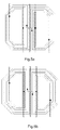
- FIG.4A Balun drawing of the proposed invention. Reference numbers are explained above in detail.
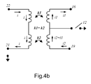
- Fig. 4B Equivalent electrical schematic relative to the balun given in Fig.4A . Note that the induced differential current is the same on both output branches (16, 19). In more detail, fig.4 describes a balun having:
- the balun has equal primary turns between left and right sides, which is advantageous over the prior art.
- the balun has equal secondary turns between left and right sides, which is advantageous over the prior art.
- the primary and secondary loops have equal resistive and capacitive equivalent parasitic components, on left and right sides of the balun, which is advantageous over the prior art.
- the magnetic coupling between primary and secondary loops has equal values, on left and right loops of the balun, which is advantageous over the prior art.
- balun's balanced internal terminals (17, 20) are connected to external terminals (16, 19) with another metal layer (15, 18) crossing the full layout, such to present equal capacitive loads to the primary/secondary, left and right loops.
- connections with another metal layer (15, 18) are connected to the balanced internal terminals (17, 20) at the middle axis level of the balun's layout, such to present equal resistive paths to left and right loops.
- the balanced balun's middle point (13) is connected outwardly with an inferior metal layer (14), crossing the full layout, such to present equal capacitive loads to the primary/secondary, left and right loops.
- the balun presents highly differential balanced impedance, whether used as single-ended to differential transformer, or vice-versa, which is advantageous over the prior art.
- the balun features low insertion loss, whether used as single-ended to differential transformer, or vice- versa, which is advantageous over the prior art.
- balun In the case where the balun is used as differential to single-ended transformer, it features high common mode rejection which is advantageous over the prior art.
- baluns may have one turn per eye, two turns, three turns, etc., and varying other characteristics, to achieve a varying impedance transformation ratio. Such options are typically not provided with prior art baluns.
- Fig. 7 Another example of unbalanced terminals connection on the same device's side, with reduced parasitic capacitance among connections and balun's turns.
- the superposed areas between terminals connection and the internal turns of the balun's core are lessened in this example compared to the previous examples. This helps to reduce the global capacitive parasitics and the electrical losses due to that.
- figs 5-7 show further examples of the present balun, detailed in fig.4 . Further observations relating to these figures are given below.
- the present balun is built with interlaced primary and secondary loops, such as to achieve maximum magnetic flux transfer and minimum insertion loss.
- the balanced loops (10) of the balun are drawn with clear wires
- the unbalanced loops (11) are drawn with dotted wires in figs (4A , 5A & 5B ), although they preferably correspond both to the same metal layer.
- the dashed wires correspond to another connection metal layer (14, 15 & 18).
- the primary loop preferably corresponds to the unbalanced loop (11), and the secondary loop preferably to the balanced loop (10), or as differential to single transformer: the primary loop corresponds to the balanced loop (10), and the secondary loop to the unbalanced loop (11).
- the balun is preferably built such to have equal primary turns between left and right sides.
- the balun is preferably built such to have equal secondary turns between left and right sides.
- the balun is preferably built such to have the geometrical and electrical middle points of primary and secondary loops (13) superposed and located at the same level.
- the balun's primary and secondary loops preferably have substantially equal resistive and capacitive components, on left and right sides.
- the magnetic coupling between the primary and secondary loops has substantially equal values, on left and right loops.
- balun's balanced internal terminals (17, 20) are connected to external terminals (16, 19) with another metal layer (15, 18) crossing the full layout, such to present substantially equal capacitive loads to the primary/secondary, left and right loops. Also, these connections with another metal layer (15, 18) are connected to the balanced internal terminals (17, 20) at the middle axis level of the balun's layout, such to present substantially equal resistive paths to left and right loops.
- the balun is designed with respect to an eight-shaped structure.
- the currents, as shown in figure 4A have opposite directions in the left and right turns, respectively through the primary and secondary loops, such to substantially reduce the outside magnetic field radiation and increase the internal mutual coupling. This increases also the balun's immunity against radiated magnetic fields or interferes caused by other sources.
- Figs 6A, 6B , 6C and 7 provide examples of flexibility in connecting the unbalanced terminals on any side (same or opposite than balanced terminals, jointly or in crossed configuration, orthogonal or diagonal sides), with respect to the substantially same layout techniques, features and advantages presented previously.
Landscapes
- Engineering & Computer Science (AREA)
- Power Engineering (AREA)
- Microelectronics & Electronic Packaging (AREA)
- Coils Or Transformers For Communication (AREA)
Claims (8)
- Balun (BALanced-to-UNbalanced) symétrique en forme de huit comprenant un premier et un deuxième oeil (A, B),
dans lequel chaque oeil (A, B) comprend des pistes conductrices (10, 11) formant des spires,
dans lequel les yeux (A, B) comprennent un nombre égal de spires primaires (11), dans lesquelles, lorsque ces spires primaires (11) sont en fonctionnement, un courant électrique circule dans une première direction dans le premier oeil (A) et dans une deuxième direction dans le deuxième oeil (B),
lesquelles spires primaires (11) forment un premier chemin de conduction d'une première extrémité de raccordement (22) à une deuxième extrémité de raccordement (21),
où les yeux (A, B) comprennent en outre un nombre égal de spires secondaires (10), dans lesquelles, lorsque ces spires secondaires (10) sont en fonctionnement, un courant électrique circule dans une première direction dans le premier oeil (A) et dans une deuxième direction dans le deuxième oeil (B),
lesquelles spires secondaires (10) forment un deuxième chemin de conduction d'une troisième extrémité de raccordement (19) à une quatrième extrémité de raccordement (16),
où les points milieux géométriques et électriques (13) des spires primaires et secondaires (10, 11) sont tous superposés et sont placés en outre dans le même plan dans le balun,
et où le balun comprend en outre des extrémités de raccordement internes équilibrées (17, 20) dans une couche métallique (15, 18) lesquelles extrémités de raccordement (17, 20) sont raccordées aux troisième et quatrième extrémités de raccordement (16, 19), en utilisant des chemins dans une autre couche métallique (15, 18) qu'une couche métallique supérieure pour dessiner le corps principal du balun, caractérisé en ce que
chacun desdits chemins dans l'autre couche métallique (15, 18) traversent la topologie du balun de part en part, de manière à fournir des charges capacitives pratiquement égales respectivement aux spires primaires et secondaires (10, 11), et respectivement au premier oeil et au deuxième oeil (A, B). - Balun symétrique en forme de huit selon la revendication 1, dans lequel les spires primaires et secondaires (10, 11) ont pratiquement la même composante de résistance électrique et pratiquement la même composante de capacité parasite.
- Balun symétrique en forme de huit selon la revendication 1 ou la revendication 2, dans lequel un couplage magnétique entre les spires primaires et secondaires (10, 11) a la même valeur au niveau des premier et deuxième yeux (A, B) du balun.
- Balun symétrique en forme de huit selon l'une quelconque des revendications 1-3, dans lequel des connexions avec l'autre couche métallique (15, 18) sont raccordées aux extrémités de raccordement internes équilibrées (17, 20) au niveau de l'axe central de la topologie du balun, de manière à présenter des chemins de résistance égale vers les premier et deuxième yeux (A, B).
- Balun symétrique en forme de huit selon l'une quelconque des revendications 1-4, comprenant en outre une couche métallique inférieure (14), dans laquelle le point milieu (13) du balun équilibré est raccordé vers l'extérieur à l'aide de la couche métallique inférieure (14), traversant de part en part la topologie, de manière à présenter des charges capacitives égales respectivement aux spires primaires et secondaires (10, 11) et au premier oeil et au deuxième oeil (A, B).
- Modem sans fil, récepteurs de radiodiffusion, émetteurs de radiodiffusion, dispositif de conversion de signaux asymétriques en signaux différentielles et vice-versa, ou transformateur d'impédance, ou toute combinaison de ceux-ci, comprenant un balun symétrique en forme de huit selon l'une quelconque des revendications 1-5.
- Dispositif, plus spécifiquement un dispositif radio comme pour un espace mobile ou portable, tel que WiMax/Wibro, Tvom, GSM, EDGE, UMTS, CDMA, Bluetooth, LAN sans fil, ou récepteurs, tel qu'un récepteur de télévision, récepteur de radiodiffusion FM, antenne dipôle et ligne de transmission en parallèle, comprenant un balun symétrique en forme de huit selon l'une quelconque des revendications 1-5.
- Dispositif de communications ou dispositif asymétrique pour la conversion en signaux différentielles ou vice-versa, comprenant un balun symétrique en forme de huit selon l'une quelconque des revendications 1-5.
Priority Applications (1)
| Application Number | Priority Date | Filing Date | Title |
|---|---|---|---|
| EP09753866.4A EP2281292B1 (fr) | 2008-05-29 | 2009-05-26 | Symetriseur radiofrequence en forme de huit |
Applications Claiming Priority (3)
| Application Number | Priority Date | Filing Date | Title |
|---|---|---|---|
| EP08157203 | 2008-05-29 | ||
| PCT/EP2009/056355 WO2009144211A1 (fr) | 2008-05-29 | 2009-05-26 | Symétriseur radiofréquence en forme de huit |
| EP09753866.4A EP2281292B1 (fr) | 2008-05-29 | 2009-05-26 | Symetriseur radiofrequence en forme de huit |
Publications (2)
| Publication Number | Publication Date |
|---|---|
| EP2281292A1 EP2281292A1 (fr) | 2011-02-09 |
| EP2281292B1 true EP2281292B1 (fr) | 2016-08-10 |
Family
ID=40970815
Family Applications (1)
| Application Number | Title | Priority Date | Filing Date |
|---|---|---|---|
| EP09753866.4A Not-in-force EP2281292B1 (fr) | 2008-05-29 | 2009-05-26 | Symetriseur radiofrequence en forme de huit |
Country Status (5)
| Country | Link |
|---|---|
| US (1) | US8427388B2 (fr) |
| EP (1) | EP2281292B1 (fr) |
| JP (1) | JP5463351B2 (fr) |
| CN (1) | CN102084439A (fr) |
| WO (1) | WO2009144211A1 (fr) |
Families Citing this family (57)
| Publication number | Priority date | Publication date | Assignee | Title |
|---|---|---|---|---|
| US8570233B2 (en) | 2010-09-29 | 2013-10-29 | Laird Technologies, Inc. | Antenna assemblies |
| JP5686353B2 (ja) | 2010-12-23 | 2015-03-18 | マーベル ワールド トレード リミテッド | 8の字バラン |
| US8717242B2 (en) * | 2011-02-15 | 2014-05-06 | Raytheon Company | Method for controlling far field radiation from an antenna |
| US8711532B2 (en) * | 2011-08-24 | 2014-04-29 | Nxp, B.V. | Integrated advance copper fuse combined with ESD/over-voltage/reverse polarity protection |
| US8742880B2 (en) * | 2011-10-28 | 2014-06-03 | Qualcomm Incorporated | Single differential transformer core |
| JP2013197988A (ja) | 2012-03-21 | 2013-09-30 | Advantest Corp | 無線通信装置および無線通信システム |
| US9312060B2 (en) * | 2012-09-20 | 2016-04-12 | Marvell World Trade Ltd. | Transformer circuits having transformers with figure eight and double figure eight nested structures |
| US9793616B2 (en) | 2012-11-19 | 2017-10-17 | Apple Inc. | Shared antenna structures for near-field communications and non-near-field communications circuitry |
| CN103199683B (zh) * | 2013-03-06 | 2016-04-06 | 广东欧珀移动通信有限公司 | 电源地线结构及电源地线的布图方法 |
| US9300022B2 (en) * | 2013-04-05 | 2016-03-29 | Scientific Components Corporation | Vaisman baluns and microwave devices employing the same |
| EP2814113B1 (fr) * | 2013-06-14 | 2019-08-07 | Ampleon Netherlands B.V. | Symétriseur de marchand et amplificateur de puissance l'utilisant |
| CN103337682B (zh) * | 2013-07-24 | 2015-03-25 | 东南大学 | 一种宽带、低损耗、高平衡度的片上巴伦 |
| US9312927B2 (en) * | 2013-11-11 | 2016-04-12 | Qualcomm Incorporated | Tunable guard ring for improved circuit isolation |
| EP2887364B1 (fr) * | 2013-12-18 | 2017-06-07 | Nxp B.V. | Transformateur intégré |
| US9697938B2 (en) * | 2014-01-17 | 2017-07-04 | Marvell World Trade Ltd. | Pseudo-8-shaped inductor |
| US9325080B2 (en) * | 2014-03-03 | 2016-04-26 | Apple Inc. | Electronic device with shared antenna structures and balun |
| US9621230B2 (en) | 2014-03-03 | 2017-04-11 | Apple Inc. | Electronic device with near-field antennas |
| US10312593B2 (en) | 2014-04-16 | 2019-06-04 | Apple Inc. | Antennas for near-field and non-near-field communications |
| US9543068B2 (en) * | 2014-06-17 | 2017-01-10 | Qualcomm Technologies International, Ltd. | Inductor structure and application thereof |
| US20160125995A1 (en) * | 2014-10-31 | 2016-05-05 | Qualcomm Incorporated | Array of interleaved 8-shaped transformers with high isolation between adjacent elements |
| US9576718B2 (en) * | 2015-06-22 | 2017-02-21 | Qualcomm Incorporated | Inductor structure in a semiconductor device |
| EP3109935B1 (fr) * | 2015-06-26 | 2019-11-27 | IMEC vzw | Élément de couplage pour coupleur hybride différentiel |
| TWI553676B (zh) * | 2015-07-07 | 2016-10-11 | 瑞昱半導體股份有限公司 | 平面式變壓器及平衡不平衡轉換器之結構 |
| TWI541842B (zh) * | 2015-10-23 | 2016-07-11 | 瑞昱半導體股份有限公司 | 螺旋狀堆疊式積體變壓器及電感 |
| US10270427B2 (en) | 2015-12-07 | 2019-04-23 | Qorvo International Pte. Ltd. | On-chip balun circuit and multi-port antenna switch circuit |
| JP6551256B2 (ja) * | 2016-02-17 | 2019-07-31 | Tdk株式会社 | コイル部品、コイル部品を内蔵した回路基板、並びに、コイル部品を備える電源回路 |
| US9843301B1 (en) | 2016-07-14 | 2017-12-12 | Northrop Grumman Systems Corporation | Silicon transformer balun |
| US10122057B2 (en) * | 2016-09-25 | 2018-11-06 | International Business Machines Corporation | Bandwidth increase method for differential passive elements |
| US11049639B2 (en) * | 2017-02-13 | 2021-06-29 | Analog Devices, Inc. | Coupled coils with lower far field radiation and higher noise immunity |
| CN106910992A (zh) * | 2017-03-02 | 2017-06-30 | 上海德门电子科技有限公司 | 应用在近场通讯的多面板四端口的fpc天线 |
| KR102209324B1 (ko) * | 2017-04-10 | 2021-01-28 | 텔레폰악티에볼라겟엘엠에릭슨(펍) | 통합형 트랜스포머 |
| GB201705913D0 (en) | 2017-04-12 | 2017-05-24 | Novelda As | Filter |
| TWI598899B (zh) * | 2017-05-11 | 2017-09-11 | 瑞昱半導體股份有限公司 | 電感裝置 |
| TWI634570B (zh) * | 2017-06-19 | 2018-09-01 | 瑞昱半導體股份有限公司 | 非對稱式螺旋狀電感 |
| CN107543977A (zh) * | 2017-09-28 | 2018-01-05 | 浙江天创信测通信科技有限公司 | 一种各向同性电磁场传感器 |
| US10622136B2 (en) * | 2017-10-26 | 2020-04-14 | Arm Ltd | Balanced-to-unbalanced (balun) transformer |
| TWI643216B (zh) * | 2017-11-10 | 2018-12-01 | 瑞昱半導體股份有限公司 | 積體電感 |
| WO2019127133A1 (fr) * | 2017-12-27 | 2019-07-04 | 华为技术有限公司 | Transformateur |
| TWI643218B (zh) * | 2018-01-05 | 2018-12-01 | 瑞昱半導體股份有限公司 | 堆疊型電感裝置 |
| TWI645426B (zh) | 2018-03-07 | 2018-12-21 | 瑞昱半導體股份有限公司 | 電感裝置 |
| US10991503B2 (en) * | 2018-07-24 | 2021-04-27 | Realtek Semiconductor Corp. | Method of fabricating an inductor |
| JP6954478B2 (ja) * | 2018-08-17 | 2021-10-27 | 株式会社村田製作所 | 平面アレイコイル及びスイッチング電源装置 |
| US11300598B2 (en) | 2018-11-26 | 2022-04-12 | Tom Lavedas | Alternative near-field gradient probe for the suppression of radio frequency interference |
| TWI703591B (zh) * | 2019-03-29 | 2020-09-01 | 瑞昱半導體股份有限公司 | 電感裝置 |
| CN110739517B (zh) * | 2019-10-31 | 2021-05-25 | 南通大学 | 一种一分三路单端-平衡式微波滤波功率分配系统 |
| CN112787595B (zh) * | 2019-11-06 | 2023-09-08 | 瑞芯微电子股份有限公司 | 信号调理方法及信号调理电路 |
| TWI697920B (zh) * | 2019-12-31 | 2020-07-01 | 瑞昱半導體股份有限公司 | 積體電感 |
| US11600916B2 (en) * | 2020-02-18 | 2023-03-07 | Qualcomm Incorporated | Area-efficient balun |
| TWI703589B (zh) * | 2020-05-11 | 2020-09-01 | 瑞昱半導體股份有限公司 | 堆疊式電感裝置 |
| TWI727815B (zh) * | 2020-05-29 | 2021-05-11 | 瑞昱半導體股份有限公司 | 積體電路 |
| CN113764581B (zh) * | 2020-06-05 | 2024-09-17 | 瑞昱半导体股份有限公司 | 集成电路 |
| TWI763560B (zh) | 2021-07-20 | 2022-05-01 | 瑞昱半導體股份有限公司 | 電感裝置 |
| US11984922B2 (en) | 2021-11-30 | 2024-05-14 | Raytheon Company | Differential probe with single transceiver antenna |
| FR3144710B1 (fr) * | 2022-12-29 | 2025-09-19 | Thales Sa | Balun Rat-Race et procédé de réduction d'encombrement de Balun Rat-Race associé |
| CN117525796B (zh) * | 2023-10-25 | 2024-11-22 | 隔空微电子(深圳)有限公司 | 一种功率分配器及多路功率分配装置 |
| CN120880342B (zh) * | 2025-09-29 | 2025-12-09 | 中科海高(成都)电子技术有限公司 | 一种无源双平衡混频器 |
| CN121148869B (zh) * | 2025-11-18 | 2026-03-31 | 荣湃半导体(上海)有限公司 | 一种平面变压器 |
Family Cites Families (10)
| Publication number | Priority date | Publication date | Assignee | Title |
|---|---|---|---|---|
| JP2773617B2 (ja) * | 1993-12-17 | 1998-07-09 | 株式会社村田製作所 | バルントランス |
| US5477204A (en) * | 1994-07-05 | 1995-12-19 | Motorola, Inc. | Radio frequency transformer |
| US5451914A (en) * | 1994-07-05 | 1995-09-19 | Motorola, Inc. | Multi-layer radio frequency transformer |
| JPH0963848A (ja) * | 1995-08-29 | 1997-03-07 | Soshin Denki Kk | 積層インダクタ |
| US6097273A (en) * | 1999-08-04 | 2000-08-01 | Lucent Technologies Inc. | Thin-film monolithic coupled spiral balun transformer |
| JP2004282412A (ja) * | 2003-03-17 | 2004-10-07 | Renesas Technology Corp | 高周波電子回路部品 |
| JP3717905B2 (ja) * | 2003-07-04 | 2005-11-16 | 三菱電機株式会社 | バランおよびミクサ |
| FR2862158B1 (fr) * | 2003-11-07 | 2006-11-17 | St Microelectronics Sa | Balun distribue a rapport d'impedance non unitaire |
| FR2894062B1 (fr) * | 2005-11-30 | 2011-06-03 | St Microelectronics Sa | Balun a rapport d'impedances 1/4 |
| FR2902933B1 (fr) * | 2006-06-22 | 2008-09-05 | St Microelectronics Sa | Combineur/diviseur de puissance |
-
2009
- 2009-05-26 WO PCT/EP2009/056355 patent/WO2009144211A1/fr not_active Ceased
- 2009-05-26 CN CN200980125097.6A patent/CN102084439A/zh active Pending
- 2009-05-26 JP JP2011510981A patent/JP5463351B2/ja not_active Expired - Fee Related
- 2009-05-26 EP EP09753866.4A patent/EP2281292B1/fr not_active Not-in-force
-
2010
- 2010-11-23 US US12/953,138 patent/US8427388B2/en active Active - Reinstated
Also Published As
| Publication number | Publication date |
|---|---|
| US20110148733A1 (en) | 2011-06-23 |
| WO2009144211A1 (fr) | 2009-12-03 |
| JP5463351B2 (ja) | 2014-04-09 |
| US8427388B2 (en) | 2013-04-23 |
| EP2281292A1 (fr) | 2011-02-09 |
| CN102084439A (zh) | 2011-06-01 |
| JP2011523509A (ja) | 2011-08-11 |
Similar Documents
| Publication | Publication Date | Title |
|---|---|---|
| EP2281292B1 (fr) | Symetriseur radiofrequence en forme de huit | |
| US10461717B2 (en) | Baluns for RF signal conversion and impedance matching | |
| US8198970B2 (en) | Transformers, balanced-unbalanced transformers (baluns) and integrated circuits including the same | |
| US6801114B2 (en) | Integrated radio having on-chip transformer balun | |
| US7526256B2 (en) | Transformer-based multi-band RF front-end architecture | |
| US7088214B2 (en) | On-chip multiple tap transformer and inductor | |
| US8044756B2 (en) | Programmable inductor | |
| US7253712B1 (en) | Integrated high frequency balanced-to-unbalanced transformers | |
| US11862381B2 (en) | Power transformer of the symmetric-asymmetric type with a fully-balanced topology | |
| EP2947767B1 (fr) | Mélangeur rf/micro-ondes/millimétrique intégré à large bande avec un ou des balun(s) intégré(s) | |
| TW201342818A (zh) | 共用多繞組變壓器的收發器 | |
| CN110752860A (zh) | 电感器电路及无线通信装置 | |
| US7439842B2 (en) | Laminated balun transformer | |
| CN118073064B (zh) | 射频叠层变压器、输出匹配网络及射频功率放大器 | |
| CN115529017B (zh) | 一种宽带巴伦阻抗变换器及包括其的电子产品 | |
| CN110098817A (zh) | 共模滤波器 | |
| CN220172349U (zh) | 巴伦以及射频前端模组 | |
| US20230230764A1 (en) | Offset transformer structure | |
| CN117318653A (zh) | 一种宽带巴伦阻抗变换器及电子产品 | |
| US20090045885A1 (en) | Passive structure for high power and low loss applications |
Legal Events
| Date | Code | Title | Description |
|---|---|---|---|
| PUAI | Public reference made under article 153(3) epc to a published international application that has entered the european phase |
Free format text: ORIGINAL CODE: 0009012 |
|
| 17P | Request for examination filed |
Effective date: 20101206 |
|
| AK | Designated contracting states |
Kind code of ref document: A1 Designated state(s): AT BE BG CH CY CZ DE DK EE ES FI FR GB GR HR HU IE IS IT LI LT LU LV MC MK MT NL NO PL PT RO SE SI SK TR |
|
| AX | Request for extension of the european patent |
Extension state: AL BA RS |
|
| DAX | Request for extension of the european patent (deleted) | ||
| 17Q | First examination report despatched |
Effective date: 20150220 |
|
| RAP1 | Party data changed (applicant data changed or rights of an application transferred) |
Owner name: ST-ERICSSON SA |
|
| GRAP | Despatch of communication of intention to grant a patent |
Free format text: ORIGINAL CODE: EPIDOSNIGR1 |
|
| INTG | Intention to grant announced |
Effective date: 20160415 |
|
| GRAS | Grant fee paid |
Free format text: ORIGINAL CODE: EPIDOSNIGR3 |
|
| GRAA | (expected) grant |
Free format text: ORIGINAL CODE: 0009210 |
|
| AK | Designated contracting states |
Kind code of ref document: B1 Designated state(s): AT BE BG CH CY CZ DE DK EE ES FI FR GB GR HR HU IE IS IT LI LT LU LV MC MK MT NL NO PL PT RO SE SI SK TR |
|
| REG | Reference to a national code |
Ref country code: GB Ref legal event code: FG4D |
|
| REG | Reference to a national code |
Ref country code: CH Ref legal event code: EP Ref country code: AT Ref legal event code: REF Ref document number: 819692 Country of ref document: AT Kind code of ref document: T Effective date: 20160815 |
|
| REG | Reference to a national code |
Ref country code: IE Ref legal event code: FG4D |
|
| REG | Reference to a national code |
Ref country code: DE Ref legal event code: R096 Ref document number: 602009040256 Country of ref document: DE |
|
| REG | Reference to a national code |
Ref country code: NL Ref legal event code: FP |
|
| REG | Reference to a national code |
Ref country code: LT Ref legal event code: MG4D |
|
| REG | Reference to a national code |
Ref country code: DE Ref legal event code: R082 Ref document number: 602009040256 Country of ref document: DE Representative=s name: GRUENECKER PATENT- UND RECHTSANWAELTE PARTG MB, DE Ref country code: DE Ref legal event code: R081 Ref document number: 602009040256 Country of ref document: DE Owner name: OCT CIRCUIT TECHNOLOGIES INTERNATIONAL LTD., IE Free format text: FORMER OWNER: ST-ERICSSON SA, PLAN-LES-OUATES, CH |
|
| REG | Reference to a national code |
Ref country code: AT Ref legal event code: MK05 Ref document number: 819692 Country of ref document: AT Kind code of ref document: T Effective date: 20160810 |
|
| PG25 | Lapsed in a contracting state [announced via postgrant information from national office to epo] |
Ref country code: FI Free format text: LAPSE BECAUSE OF FAILURE TO SUBMIT A TRANSLATION OF THE DESCRIPTION OR TO PAY THE FEE WITHIN THE PRESCRIBED TIME-LIMIT Effective date: 20160810 Ref country code: NO Free format text: LAPSE BECAUSE OF FAILURE TO SUBMIT A TRANSLATION OF THE DESCRIPTION OR TO PAY THE FEE WITHIN THE PRESCRIBED TIME-LIMIT Effective date: 20161110 Ref country code: IS Free format text: LAPSE BECAUSE OF FAILURE TO SUBMIT A TRANSLATION OF THE DESCRIPTION OR TO PAY THE FEE WITHIN THE PRESCRIBED TIME-LIMIT Effective date: 20161210 Ref country code: HR Free format text: LAPSE BECAUSE OF FAILURE TO SUBMIT A TRANSLATION OF THE DESCRIPTION OR TO PAY THE FEE WITHIN THE PRESCRIBED TIME-LIMIT Effective date: 20160810 Ref country code: IT Free format text: LAPSE BECAUSE OF FAILURE TO SUBMIT A TRANSLATION OF THE DESCRIPTION OR TO PAY THE FEE WITHIN THE PRESCRIBED TIME-LIMIT Effective date: 20160810 Ref country code: LT Free format text: LAPSE BECAUSE OF FAILURE TO SUBMIT A TRANSLATION OF THE DESCRIPTION OR TO PAY THE FEE WITHIN THE PRESCRIBED TIME-LIMIT Effective date: 20160810 |
|
| PG25 | Lapsed in a contracting state [announced via postgrant information from national office to epo] |
Ref country code: ES Free format text: LAPSE BECAUSE OF FAILURE TO SUBMIT A TRANSLATION OF THE DESCRIPTION OR TO PAY THE FEE WITHIN THE PRESCRIBED TIME-LIMIT Effective date: 20160810 Ref country code: AT Free format text: LAPSE BECAUSE OF FAILURE TO SUBMIT A TRANSLATION OF THE DESCRIPTION OR TO PAY THE FEE WITHIN THE PRESCRIBED TIME-LIMIT Effective date: 20160810 Ref country code: GR Free format text: LAPSE BECAUSE OF FAILURE TO SUBMIT A TRANSLATION OF THE DESCRIPTION OR TO PAY THE FEE WITHIN THE PRESCRIBED TIME-LIMIT Effective date: 20161111 Ref country code: LV Free format text: LAPSE BECAUSE OF FAILURE TO SUBMIT A TRANSLATION OF THE DESCRIPTION OR TO PAY THE FEE WITHIN THE PRESCRIBED TIME-LIMIT Effective date: 20160810 Ref country code: PL Free format text: LAPSE BECAUSE OF FAILURE TO SUBMIT A TRANSLATION OF THE DESCRIPTION OR TO PAY THE FEE WITHIN THE PRESCRIBED TIME-LIMIT Effective date: 20160810 Ref country code: SE Free format text: LAPSE BECAUSE OF FAILURE TO SUBMIT A TRANSLATION OF THE DESCRIPTION OR TO PAY THE FEE WITHIN THE PRESCRIBED TIME-LIMIT Effective date: 20160810 Ref country code: PT Free format text: LAPSE BECAUSE OF FAILURE TO SUBMIT A TRANSLATION OF THE DESCRIPTION OR TO PAY THE FEE WITHIN THE PRESCRIBED TIME-LIMIT Effective date: 20161212 |
|
| REG | Reference to a national code |
Ref country code: FR Ref legal event code: PLFP Year of fee payment: 9 |
|
| PG25 | Lapsed in a contracting state [announced via postgrant information from national office to epo] |
Ref country code: RO Free format text: LAPSE BECAUSE OF FAILURE TO SUBMIT A TRANSLATION OF THE DESCRIPTION OR TO PAY THE FEE WITHIN THE PRESCRIBED TIME-LIMIT Effective date: 20160810 Ref country code: EE Free format text: LAPSE BECAUSE OF FAILURE TO SUBMIT A TRANSLATION OF THE DESCRIPTION OR TO PAY THE FEE WITHIN THE PRESCRIBED TIME-LIMIT Effective date: 20160810 |
|
| REG | Reference to a national code |
Ref country code: DE Ref legal event code: R097 Ref document number: 602009040256 Country of ref document: DE |
|
| PG25 | Lapsed in a contracting state [announced via postgrant information from national office to epo] |
Ref country code: DK Free format text: LAPSE BECAUSE OF FAILURE TO SUBMIT A TRANSLATION OF THE DESCRIPTION OR TO PAY THE FEE WITHIN THE PRESCRIBED TIME-LIMIT Effective date: 20160810 Ref country code: SK Free format text: LAPSE BECAUSE OF FAILURE TO SUBMIT A TRANSLATION OF THE DESCRIPTION OR TO PAY THE FEE WITHIN THE PRESCRIBED TIME-LIMIT Effective date: 20160810 Ref country code: BG Free format text: LAPSE BECAUSE OF FAILURE TO SUBMIT A TRANSLATION OF THE DESCRIPTION OR TO PAY THE FEE WITHIN THE PRESCRIBED TIME-LIMIT Effective date: 20161110 Ref country code: CZ Free format text: LAPSE BECAUSE OF FAILURE TO SUBMIT A TRANSLATION OF THE DESCRIPTION OR TO PAY THE FEE WITHIN THE PRESCRIBED TIME-LIMIT Effective date: 20160810 Ref country code: BE Free format text: LAPSE BECAUSE OF FAILURE TO SUBMIT A TRANSLATION OF THE DESCRIPTION OR TO PAY THE FEE WITHIN THE PRESCRIBED TIME-LIMIT Effective date: 20160810 |
|
| PLBE | No opposition filed within time limit |
Free format text: ORIGINAL CODE: 0009261 |
|
| STAA | Information on the status of an ep patent application or granted ep patent |
Free format text: STATUS: NO OPPOSITION FILED WITHIN TIME LIMIT |
|
| PGFP | Annual fee paid to national office [announced via postgrant information from national office to epo] |
Ref country code: NL Payment date: 20170421 Year of fee payment: 9 |
|
| 26N | No opposition filed |
Effective date: 20170511 |
|
| PGFP | Annual fee paid to national office [announced via postgrant information from national office to epo] |
Ref country code: FR Payment date: 20170421 Year of fee payment: 9 Ref country code: GB Payment date: 20170426 Year of fee payment: 9 Ref country code: DE Payment date: 20170420 Year of fee payment: 9 |
|
| REG | Reference to a national code |
Ref country code: NL Ref legal event code: PD Owner name: OCT CIRCUIT TECHNOLOGIES INTERNATIONAL LIMITED; IE Free format text: DETAILS ASSIGNMENT: CHANGE OF OWNER(S), ASSIGNMENT; FORMER OWNER NAME: ST-ERICSSON SA Effective date: 20170620 |
|
| PG25 | Lapsed in a contracting state [announced via postgrant information from national office to epo] |
Ref country code: SI Free format text: LAPSE BECAUSE OF FAILURE TO SUBMIT A TRANSLATION OF THE DESCRIPTION OR TO PAY THE FEE WITHIN THE PRESCRIBED TIME-LIMIT Effective date: 20160810 Ref country code: LU Free format text: LAPSE BECAUSE OF NON-PAYMENT OF DUE FEES Effective date: 20170531 |
|
| REG | Reference to a national code |
Ref country code: CH Ref legal event code: PL |
|
| PG25 | Lapsed in a contracting state [announced via postgrant information from national office to epo] |
Ref country code: MC Free format text: LAPSE BECAUSE OF FAILURE TO SUBMIT A TRANSLATION OF THE DESCRIPTION OR TO PAY THE FEE WITHIN THE PRESCRIBED TIME-LIMIT Effective date: 20160810 |
|
| REG | Reference to a national code |
Ref country code: FR Ref legal event code: TP Owner name: OCT CIRCUIT TECHNOLOGIES INTERNATIONAL LIMITED, IE Effective date: 20180116 |
|
| REG | Reference to a national code |
Ref country code: IE Ref legal event code: MM4A |
|
| PG25 | Lapsed in a contracting state [announced via postgrant information from national office to epo] |
Ref country code: CH Free format text: LAPSE BECAUSE OF NON-PAYMENT OF DUE FEES Effective date: 20170531 Ref country code: LI Free format text: LAPSE BECAUSE OF NON-PAYMENT OF DUE FEES Effective date: 20170531 |
|
| PG25 | Lapsed in a contracting state [announced via postgrant information from national office to epo] |
Ref country code: LU Free format text: LAPSE BECAUSE OF NON-PAYMENT OF DUE FEES Effective date: 20170526 |
|
| PG25 | Lapsed in a contracting state [announced via postgrant information from national office to epo] |
Ref country code: IE Free format text: LAPSE BECAUSE OF NON-PAYMENT OF DUE FEES Effective date: 20170526 |
|
| PG25 | Lapsed in a contracting state [announced via postgrant information from national office to epo] |
Ref country code: MT Free format text: LAPSE BECAUSE OF NON-PAYMENT OF DUE FEES Effective date: 20170526 |
|
| REG | Reference to a national code |
Ref country code: DE Ref legal event code: R119 Ref document number: 602009040256 Country of ref document: DE |
|
| REG | Reference to a national code |
Ref country code: NL Ref legal event code: MM Effective date: 20180601 |
|
| GBPC | Gb: european patent ceased through non-payment of renewal fee |
Effective date: 20180526 |
|
| PG25 | Lapsed in a contracting state [announced via postgrant information from national office to epo] |
Ref country code: FR Free format text: LAPSE BECAUSE OF NON-PAYMENT OF DUE FEES Effective date: 20180531 Ref country code: NL Free format text: LAPSE BECAUSE OF NON-PAYMENT OF DUE FEES Effective date: 20180601 Ref country code: GB Free format text: LAPSE BECAUSE OF NON-PAYMENT OF DUE FEES Effective date: 20180526 Ref country code: DE Free format text: LAPSE BECAUSE OF NON-PAYMENT OF DUE FEES Effective date: 20181201 |
|
| PG25 | Lapsed in a contracting state [announced via postgrant information from national office to epo] |
Ref country code: HU Free format text: LAPSE BECAUSE OF FAILURE TO SUBMIT A TRANSLATION OF THE DESCRIPTION OR TO PAY THE FEE WITHIN THE PRESCRIBED TIME-LIMIT; INVALID AB INITIO Effective date: 20090526 |
|
| PG25 | Lapsed in a contracting state [announced via postgrant information from national office to epo] |
Ref country code: CY Free format text: LAPSE BECAUSE OF NON-PAYMENT OF DUE FEES Effective date: 20160810 |
|
| PG25 | Lapsed in a contracting state [announced via postgrant information from national office to epo] |
Ref country code: MK Free format text: LAPSE BECAUSE OF FAILURE TO SUBMIT A TRANSLATION OF THE DESCRIPTION OR TO PAY THE FEE WITHIN THE PRESCRIBED TIME-LIMIT Effective date: 20160810 |
|
| PG25 | Lapsed in a contracting state [announced via postgrant information from national office to epo] |
Ref country code: TR Free format text: LAPSE BECAUSE OF FAILURE TO SUBMIT A TRANSLATION OF THE DESCRIPTION OR TO PAY THE FEE WITHIN THE PRESCRIBED TIME-LIMIT Effective date: 20160810 |