EP2281326B1 - Antenne insensible à la polarisation pour des lecteurs à identification par radiofréquence manuels - Google Patents
Antenne insensible à la polarisation pour des lecteurs à identification par radiofréquence manuels Download PDFInfo
- Publication number
- EP2281326B1 EP2281326B1 EP09755634.4A EP09755634A EP2281326B1 EP 2281326 B1 EP2281326 B1 EP 2281326B1 EP 09755634 A EP09755634 A EP 09755634A EP 2281326 B1 EP2281326 B1 EP 2281326B1
- Authority
- EP
- European Patent Office
- Prior art keywords
- slot
- conductive loop
- radio frequency
- loop element
- antenna
- Prior art date
- Legal status (The legal status is an assumption and is not a legal conclusion. Google has not performed a legal analysis and makes no representation as to the accuracy of the status listed.)
- Active
Links
Images


Classifications
-
- H—ELECTRICITY
- H01—ELECTRIC ELEMENTS
- H01Q—ANTENNAS, i.e. RADIO AERIALS
- H01Q1/00—Details of, or arrangements associated with, antennas
- H01Q1/12—Supports; Mounting means
- H01Q1/22—Supports; Mounting means by structural association with other equipment or articles
- H01Q1/2208—Supports; Mounting means by structural association with other equipment or articles associated with components used in interrogation type services, i.e. in systems for information exchange between an interrogator/reader and a tag/transponder, e.g. in Radio Frequency Identification [RFID] systems
- H01Q1/2216—Supports; Mounting means by structural association with other equipment or articles associated with components used in interrogation type services, i.e. in systems for information exchange between an interrogator/reader and a tag/transponder, e.g. in Radio Frequency Identification [RFID] systems used in interrogator/reader equipment
-
- H—ELECTRICITY
- H01—ELECTRIC ELEMENTS
- H01Q—ANTENNAS, i.e. RADIO AERIALS
- H01Q13/00—Waveguide horns or mouths; Slot antennas; Leaky-waveguide antennas; Equivalent structures causing radiation along the transmission path of a guided wave
- H01Q13/10—Resonant slot antennas
- H01Q13/16—Folded slot antennas
-
- H—ELECTRICITY
- H01—ELECTRIC ELEMENTS
- H01Q—ANTENNAS, i.e. RADIO AERIALS
- H01Q21/00—Antenna arrays or systems
- H01Q21/24—Combinations of antenna units polarised in different directions for transmitting or receiving circularly and elliptically polarised waves or waves linearly polarised in any direction
-
- H—ELECTRICITY
- H01—ELECTRIC ELEMENTS
- H01Q—ANTENNAS, i.e. RADIO AERIALS
- H01Q7/00—Loop antennas with a substantially uniform current distribution around the loop and having a directional radiation pattern in a plane perpendicular to the plane of the loop
Definitions
- Embodiments of the subject matter described herein relate generally to radio frequency (RF) antennas. More particularly, embodiments of the subject matter relate to an RF antenna suitable for use with an RF identification (RFID) reader.
- RFID RF identification
- an RFID system includes two primary components: a reader (also known as an interrogator); and a tag (also known as a transponder).
- the tag is a miniature device that is capable of responding, via an air channel, to an RF signal generated by the reader.
- the tag is configured to generate a reflected RF signal in response to the RF signal emitted from the reader.
- the reflected RF signal is modulated in a manner that conveys identification data back to the reader.
- the identification data can then be stored, processed, displayed, or transmitted by the reader as needed.
- RFID reader antennas are relatively large, heavy, and obtrusive, and other RFID antennas provide either horizontal polarization or vertical polarization.
- Conventional RFID tags are typically polarized in only one direction: vertical or horizontal. Therefore, a horizontally polarized RFID reader antenna is unable to accurately read a vertically polarized tag without physical manipulation or rotation of the reader and/or tag. Likewise, a vertically polarized RFID reader antenna is unable to accurately read a horizontally polarized tag without physical manipulation or rotation of the reader and/or tag.
- JP 2003 069463 A describes a slot antenna and a loop antenna formed on a transmission circuit board as a conductor pattern being used for the mobile transmitter and a high frequency switch switches the antenna so as to allow the selected antenna to transmit the same data frame. Mounting the antennas to emit two orthogonal polarized waves on the transmitter side in this way can increase the stability of communication by the mobile transmitter.
- US 2008/042846 A1 describes an antenna for a radio frequency identification (RFID) system and a method for communicating in an RFID system.
- the antenna includes a first port configured to provide RFID communication in a first polarization plane and a second port configured to provide RFID communication in a second polarization plane.
- the first polarization plane is orthogonal to the second polarization plane.
- connection means that one element/node/feature is directly joined to (or directly communicates with) another element/node/feature, and not necessarily mechanically.
- coupled means that one element/node/feature is directly or indirectly joined to (or directly or indirectly communicates with) another element/node/feature, and not necessarily mechanically.
- An RFID reader as described herein utilizes a polarization insensitive multioperational antenna that is relatively small in size, achieves good RF performance, and is insensitive to the polarization of the RFID tags being interrogated by the RFID reader.
- the antenna design can be implemented to accommodate the packaging requirements and configuration of existing RFID reader equipment and/or to accommodate new equipment.
- conventional techniques related to RFID data transmission, RFID system architectures, RF antenna design, signal processing, and other functional aspects of the systems (and the individual operating components of the systems) may not be described in detail herein.
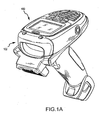
- FIG. 1A is a perspective view of a first embodiment of an RFID reader 100 that incorporates a polarization insensitive antenna component 102
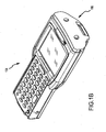
- FIG. 1B is a perspective view of a second embodiment of an RFID reader 104 that incorporates a polarization insensitive antenna component 106
- FIG. 2 is a perspective view of a third embodiment of an RFID reader 200 that incorporates a polarization insensitive antenna component 202.
- RFID reader 100 is a relatively small and compact handheld device that can be operated to interrogate RFID tags within its interrogation range.
- RFID reader 100 utilizes antenna component 102 to transmit RFID interrogation signals, and to receive response signals generated by RFID tags.
- RFID reader 100 is gun-shaped, and it uses a front-mounted antenna component 102 that is naturally pointed toward the intended target during normal handheld operation of RFID reader 100.
- RFID reader 104 is another relatively small and compact handheld device, which utilizes antenna component 106 to transmit RFID interrogation signals, and to receive response signals generated by RFID tags.
- This particular embodiment of RFID reader 104 has its antenna component 106 located at the top of the housing, to accommodate pointing toward the intended target during normal handheld operation of RFID reader 104.
- RFID reader 200 represents a hybrid device that includes antenna component 202 for purposes of supporting RFID operations.
- RFID reader 200 may include another scanning element 204 that supports non-RFID operations.
- scanning element 204 may be a wireless bar code scanner.
- the polarization insensitive antenna designs described herein can be deployed in any number of RFID reader (or mobile computing device) configurations, and the embodiments depicted in FIG. 1 and FIG. 2 are merely exemplary.
- FIG. 3 is a schematic representation of an embodiment of an RFID reader 300 that utilizes a polarization insensitive antenna.
- RFID readers 100, 104, and 200 may incorporate the arrangement depicted in FIG. 3 . It should be apparent that FIG. 3 depicts RFID reader 300 in a very simplified manner, and a practical embodiment will of course include many additional features and components.
- RFID reader 300 generally includes, without limitation: an RF communication module 302; an antenna 304 coupled to RF communication module 302; a power supply 306; a processor 308; and an appropriate amount of memory 310.
- RFID reader 300 may also include a housing, a display element, a keypad, an interrogation trigger, a touch panel, other input/output elements, or the like. The various operating elements of RFID reader are coupled together as needed to facilitate the delivery of operating power from power supply 306, the transfer of data, the transfer of control signals and commands, and the like.
- RF communication module 302 is suitably configured to process RF signals associated with the operation of RFID reader 300, and to otherwise support the RFID functions of RFID reader 300.
- RF communication module 302 may include a transceiver or radio element that generates RFID interrogation signals and receives reflected RFID signals generated by RFID tags in response to the interrogation signals.
- RF communication module 302 is suitably configured to generate the RF drive signals for antenna 304.
- RF communication module 302 is designed to operate in the UHF frequency band designated for RFID systems. Alternate embodiments may instead utilize the High Frequency band or the Low Frequency band designated for RFID systems.
- RFID systems may utilize the 902-928 MHz frequency band, and in Europe, RFID systems may utilize the 865-868 MHz frequency band.
- antenna 304 can be designed, configured, and tuned to accommodate the particular operating frequency band of the host RFID reader.
- Antenna 304 is suitably configured to transmit and receive RF energy associated with the operation of RFID reader 300. Accordingly, antenna 304 can be coupled to RF communication module 302 using two RF transmission lines 312/314.
- antenna 304 preferably includes a conductive loop element that functions as a loop antenna, and a slot formed in the conductive loop element (the slot functions as a slot antenna). Accordingly, RF transmission line 312 is utilized for the conductive loop element, and RF transmission line 314 is utilized for the slot (or vice versa).
- two-conductor RF coaxial cables can be used for RF transmission lines 312/314, in combination with suitable RF connectors, plugs, nodes, or terminals on RF communication module 302 and/or on antenna 304.
- Power supply 306 may be a disposable or rechargeable battery, a set of batteries, or a battery pack that is rated to provide the necessary voltage and energy to support the operation of RFID reader 300. Alternatively or additionally, power supply 306 may receive power from an external source such as an ordinary AC outlet.
- Processor 308 may be any general purpose microprocessor, controller, or microcontroller that is suitably configured to control the operation of RFID reader 300.
- processor 308 may execute one or more software applications that provide the desired functionality for RFID reader 300.
- processor 308 can control, manage, and regulate operation of RFID reader 300 in different polarization modes, different interrogation modes, and the like, where the different modes utilize the conductive loop and/or the radiating slot of antenna 304.
- Memory 310 may be realized as any processor-readable medium, including an electronic circuit, a semiconductor memory device, a ROM, a flash memory, an erasable ROM, a floppy diskette, a CD-ROM, an optical disk, a hard disk, an organic memory element, or the like.
- memory 310 is capable of storing application software utilized by RFID reader 300 and/or RFID data captured by RFID reader 300 during operation.
- antenna 304 may utilize a loop antenna, which can be designed to achieve a desired polarization.
- a loop antenna can be created by cutting a slot approximately one-half wavelength long in conductive material such as a copper sheet.
- This type of antenna is essentially the negative of a dipole or loop antenna because it is the absence of conductive material that creates a resonating structure, as opposed to the conductive material itself.
- the edges of the slot radiate, resulting in reversal of the electric and magnetic fields. Consequently, the polarity of a slot antenna is opposite compared to that of a loop antenna. In other words, a horizontal slot is vertically polarized, and a vertical slot is horizontally polarized.
- the technique described here utilizes a half-wavelength slot formed in the conductive material of a loop antenna.
- two orthogonal polarizations can be achieved using one antenna structure.
- the antenna structure described herein resonates the slot at the same frequency as the conductive loop element, orthogonal in polarization. Adding this second antenna element (the slot) does not increase the overall size of the antenna and, as a result, the size impact to the host RFID reader is negligible.
- FIG. 4 is a layout diagram of a first embodiment of an RF antenna 400 suitable for use in an RFID reader
- FIG. 5 is a cross sectional view of RF antenna 400 as viewed from line 5-5 in FIG. 4.
- FIG. 4 depicts a front or face view of antenna 400, as it might appear when deployed in a handheld RFID reader.
- Antenna includes a conductive loop element 402, which is preferably mounted or affixed to an appropriate substrate 404.
- Conductive loop element 402 is formed from an electrically conductive material such as, without limitation, copper, aluminum, gold, alloys thereof, or the like. In practice, conductive loop element 402 can be formed from a relatively thin sheet or printed film of metal, such as copper.
- Substrate 404 is preferably formed from a dielectric or insulating material such as, without limitation, plastic, an FR-4 circuit board, a ceramic material, a flexible vinyl material, or the like.
- substrate 404 is a distinct component of an antenna module or package, as depicted in FIG. 1 .
- substrate 404 is an integrated part of a housing, shell, or other part of the RFID reader itself.
- conductive loop element 402 may be printed on or attached to the inside wall of the overall housing of the RFID reader.
- Conductive loop element 402 corresponds to the overall conductive trace or pattern of antenna 400.
- conductive loop element 402 is generally oval shaped.
- an embodiment of antenna 400 may employ a conductive loop element having alternative shapes, e.g., circular (see FIG. 6 ), triangular, square, oblong, barbell, elliptical, etc.
- Conductive loop element 402 includes a first end 406 and a second end 408, and the length of conductive loop element 402 is generally defined as the length of its major longitudinal path between first end 406 and second end 408.
- the major longitudinal path of conductive loop element 402 corresponds to approximately one "lap" around the oval shaped route.
- Antenna 400 has a first loop signal node 410 located at or proximate to first end 406, and a second loop signal node 412 located at or proximate to second end 408.
- First loop signal node 410 and second loop signal node 412 represent the RF input/output nodes for conductive loop element 402.
- first loop signal node 410 and second loop signal node 412 are used to apply an appropriate RF drive signal to conductive loop element 402, and to provide return signals from conductive loop element 402.
- a suitably configured RF transmission line (e.g., a two-conductor coaxial cable) can be coupled to first loop signal node 410 and second loop signal node 412 to accommodate the propagation of RF energy to and from conductive loop element 402.
- a suitably configured RF transmission line e.g., a two-conductor coaxial cable
- one conductor of the RF transmission line would be coupled to first loop signal node 410, and the other conductor would be coupled to second loop signal node 412.
- Conductive loop element 402 is suitably sized, shaped, and configured to resonate at the desired frequency or frequency band with a first polarization.
- conductive loop element 402 is horizontally polarized relative to the orientation and perspective of FIG. 4 .
- Horizontal polarization is established because the loop signal nodes 410/412 of conductive loop element 402 are located at the top.
- antenna 400 were instead oriented sideways (i.e., rotated ninety degrees relative to that depicted in FIG. 4 ), then conductive loop element 402 would be vertically polarized.
- Conductive loop element 402 is tuned primarily by adjusting or selecting its length, i.e., the length of its major longitudinal path. A longer path results in a lower resonant frequency, and a shorter path results in a higher resonant frequency.
- the electrical length of conductive loop element 402 (which may be different than its physical length) should be approximately one wavelength long, referring to the desired operating frequency. Accordingly, the path length can be chosen to accommodate the particular frequency or frequency band of interest for the given RFID system.
- one wavelength corresponds to an electrical loop length of about thirteen inches, however, the physical length of conductive loop element 402 can be reduced to about four to six inches using electronic circuits, networks, and/or components (e.g., inductive and capacitive loads, baluns, etc.).
- the height 414 of conductive loop element 402 may be within the range of about 0.5 inches to about 2.5 inches, and the width 416 of conductive loop element 402 may be within the range of about 2.0 inches to about 3.5 inches.
- Antenna 400 also includes at least one slot 418 formed in conductive loop element 402.
- Slot 418 is defined by an area within conductive loop element 402 that lacks conductive material. Slot 418 creates a feature in conductive loop element 402 that operates independently of conductive loop element 402. Simply put, the loop antenna element and the slot antenna element are isolated from each other. Moreover, the impedance of conductive loop element 402 will be much lower than the impedance of slot 418, further enabling their coexistence. It is therefore not necessary to switch between the two antenna elements to make their respective feeds RF-invisible to each other.
- slot 418 is formed between first end 406 and second end 408 of conductive loop element 402, and slot 418 is generally oriented along, and is substantially in alignment with, the major longitudinal path of conductive loop element 402. In other words, slot 418 follows the shape, contour, and path of conductive loop element 402. Although not always required, slot 418 may be centered in the path of conductive loop element 402, i.e., slot is aligned with the central longitudinal axis of the path. Notably, because slot 418 follows the overall geometry of conductive loop element 402, isolation is preserved between slot 418 and conductive loop element 402. In other words, operation of slot 418 as an antenna element is unaffected by operation of conductive loop element 402 as an antenna element, and vice versa. Moreover, tuning of conductive loop element 402 is relatively independent of tuning of slot 418.
- Slot 418 includes a first end 420 and a second end 422.
- first end 420 of slot 418 is located at or proximate to first end 406 of conductive loop element
- second end 422 of slot 418 is located at or proximate to second end 408 of conductive loop element.
- the ends of slot 418 need not be co-located with the ends of conductive loop element 402.
- slot 418 is balanced and symmetrically positioned within conductive loop element 402. Such balance and symmetry is not always required, and alternate embodiments may employ a slot configuration that is offset or skewed within the loop element. However, when the slot is symmetric in the loop, the radiated pattern will tend to be more symmetric as a result.
- the preferred embodiment would have the two radiation patterns significantly overlapping, allowing the user to read both vertical and horizontal tags in the same field of view without physically manipulating the reader.
- the polarization may be affected as the slot becomes asymmetric.
- a symmetric slot inside the loop yields a slot polarization that is orthogonal to the loop polarization.
- a symmetric slot may also be easier to manufacture, and an antenna with a symmetric slot may be easier to assemble into the system.
- Antenna 400 has a first slot signal node 424 and a second slot signal node 426, which are located on conductive loop element 402.
- the location of slot signal nodes 424/426 along the path of slot 418 can affect impedance matching of antenna 400 and, therefore, the particular location may be chosen according to the specifications and characteristics of the system.
- both slot signal nodes 424/426 are located at or proximate to first end 420 of slot 418.
- slot signal nodes 424/426 may instead be located at or proximate to second end 422 of slot 418 without altering the performance of antenna 400.
- slot signal nodes 424/426 are also located at or proximate to first end 406 of conductive loop element 402.
- slot signal nodes 424/426 may instead be located at or proximate to second end 408 of conductive loop element 402 without altering the performance of antenna 400.
- Slot signal nodes 424/426 represent the RF input/output nodes for slot 418.
- slot signal nodes 424/426 are used to apply an appropriate RF drive signal to slot 418, and to provide return signals from slot 418.
- slot signal nodes 424/426 are located on opposite sides of slot 418.
- first slot signal node 424 resides at one side of slot 418
- second slot signal node 426 resides at the other side of slot 418, preferably opposite first slot signal node 424.
- a suitably configured RF transmission line (e.g., a two-conductor coaxial cable) can be coupled to first slot signal node 424 and second slot signal node 426 to accommodate the propagation of RF energy to and from slot 418.
- a suitably configured RF transmission line e.g., a two-conductor coaxial cable
- one conductor of the RF transmission line would be coupled to first slot signal node 424, and the other conductor would be coupled to second slot signal node 426.
- Slot 418 is suitably sized, shaped, and configured to resonate at the desired frequency or frequency band with a second polarization, which is different than the first polarization of conductive loop element 402.
- slot 418 is vertically polarized relative to the orientation and perspective of FIG. 4 .
- antenna 400 were instead oriented sideways (i.e., rotated ninety degrees relative to that depicted in FIG. 4 ), then slot 418 would be horizontally polarized.
- the hybrid/combined structure of antenna 400 allows it to operate in a polarization insensitive manner, where conductive loop element 402 is configured to operate as a first antenna polarized in a first orientation and where slot 418 is configured to operate as a second antenna polarized in a second orientation.
- conductive loop element 402 and slot 418 are orthogonally polarized relative to each other, and they operate as orthogonally polarized antennas.
- slot 418 is tuned such that it resonates at or near the same frequency or frequency band as conductive loop element 402.
- Slot 418 is tuned primarily by adjusting or selecting its length (i.e., the length along the major longitudinal path of conductive loop element 402) and its gap width 428. A longer path results in a lower resonant frequency, and a shorter path results in a higher resonant frequency.
- the gap width 428 of slot 418 tunes the bandwidth of slot 418: a wider gap generally results in more bandwidth, while a narrower gap generally results in less bandwidth.
- the length and gap width 428 of slot 418 can be chosen to accommodate the particular frequency or frequency band of interest for the given RFID system.
- slot 418 may be within the range of about 4.0 to 6.5 inches long and the gap width 428 of slot 418 may be within the range of about 0.025 to 0.150 inches.
- Alternate embodiments of an RF antenna as described herein can utilize more than one slot formed in a conductive loop element. Multiple slots may be used to broaden the frequency response of the antenna. In such alternate embodiments, additional slot signal nodes may also be employed (as needed) to accommodate additional RF transmission lines.
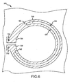
- FIG. 6 is a layout diagram of a second embodiment of an RF antenna 500 suitable for use in an RFID reader.
- Antenna 500 has several different features and characteristics, compared to antenna 400.
- antenna 500 utilizes a circular conductive loop element 502 rather than one having an oval shape.
- conductive loop element 502 is vertically polarized relative to the orientation and perspective of FIG. 5 , because the loop signal nodes 510/512 of conductive loop element 502 are located at the side.
- antenna 500 were rotated ninety degrees relative to that depicted in FIG. 6 , then conductive loop element 502 would be horizontally polarized.
- the slot 518 formed within conductive loop element 502 is not symmetric or balanced. In other words, one end 520 of slot 518 is relatively distant from the first end 506 of conductive loop element 502, while the other end 522 of slot 518 is relatively close to the second end 508 of conductive loop element 502.
- FIG. 6 depicts how slot 518 is skewed or offset within conductive loop element 502.
- FIG. 6 depicts an embodiment where the slot signal nodes 524/526 are located relatively far away from the ends 520/522 of slot 518. Moreover, slot signal nodes 524/526 need not be directly opposite each other - FIG. 6 depicts such an embodiment.
- Processor 308 may be suitably configured to control the operation of RFID reader 300 (and, in particular, RF communication module 302) in accordance with a number of different operating modes.
- RF communication module 302 may be suitably controlled and configured to drive conductive loop element 402 and to not drive slot 418 during a first operating mode (e.g., horizontal polarization mode).
- RF communication module 302 may be suitably controlled and configured to drive slot 418 and to not drive conductive loop element 402 during a second operating mode (e.g., vertical polarization mode).
- RF communication module 302 can switch between operating modes to alternately drive conductive loop element 402 with a first drive signal, and drive slot 418 with a second drive signal (the first and second drive signals in this example may be the same or different).
- This switching mode may be desirable to maintain full transmit power for both polarizations in an alternating manner.
- the switching frequency may be selected to suit the needs of the particular application.
- one polarization mode can be weighted more than the other if desired. Such weighting may be beneficial in environments where the number of horizontally polarized RFID tags is greater than the number of vertically polarized RFID tags (or vice versa).
- RFID reader 300 may be suitably configured to simultaneously drive conductive loop element 402 and slot 418 using the same drive signal or different drive signals. This is possible because at any instant of time one end of conductive loop element 402 is positive and the other end is negative, while one side of slot 418 is positive and the other side is negative.
- conductive loop element 402 and slot 418 are preferably tuned to resonate at the same frequency or frequencies and, therefore, RF communication module 302 can drive both of the orthogonally polarized antenna elements with a common RF drive signal. In practice, this allows RFID reader 300 to interrogate a group of RFID tags that may not be polarized or oriented in the same manner.
Landscapes
- Variable-Direction Aerials And Aerial Arrays (AREA)
Claims (19)
- Agencement d'antennes (400) pour un lecteur d'identification radiofréquence (100), l'agencement d'antennes comprenant :une antenne cadre conductrice configurée pour résonner en tant qu'antenne cadre à une fréquence avec une première polarisation dans une première orientation, l'antenne cadre conductrice définissant un trajet longitudinal principal étant montée sur un substrat isolant (404),l'antenne cadre conductrice comprend une première extrémité (406) et une seconde extrémité (408) et l'agencement d'antennes comprend en outre un premier noeud de signal à boucle (410) au niveau de la première extrémité et un second noeud de signal à boucle (412) au niveau de la seconde extrémité, etune fente de demi-longueur d'onde (418) étant configurée pour résonner en tant qu'antenne à fente à la fréquence avec une seconde polarisation dans une seconde orientation, les première et seconde polarisations étant orthogonales entre elles,l'agencement d'antennes comprend en outre un premier noeud de signal à fente au niveau d'un premier côté de la fente et un second noeud de signal à fente au niveau d'un second côté de la fente,caractérisé en ce que la fente est formée dans le matériau conducteur de l'antenne cadre le long du trajet longitudinal principal.
- Agencement d'antennes selon la revendication 1, dans lequel l'élément à boucle conductrice est de forme ovale.
- Agencement d'antennes selon la revendication 1, dans lequel :l'élément à boucle conductrice comprend la première extrémité (406) et la seconde extrémité (408) à proximité étroite l'une de l'autre de sorte que l'élément à boucle conductrice englobe presque complètement une zone intérieure du substrat isolant.
- Agencement d'antennes selon la revendication 1, dans lequel :l'élément à boucle conductrice comprend la première extrémité (406) et la seconde extrémité (408) à proximité étroite l'une de l'autre de sorte que l'élément à boucle conductrice englobe presque complètement une zone intérieure du substrat isolant, etla fente est formée dans l'élément à boucle conductrice entre la première extrémité et la seconde extrémité.
- Agencement d'antennes selon la revendication 1, dans lequel :la fente a une longueur d'une demi-longueur d'onde de la fréquence.
- Agencement d'antennes selon la revendication 1, ayant
le premier noeud de signal à boucle (410) positionné à proximité de la première extrémité (406) de l'élément à boucle conductrice,
le second noeud de signal à boucle (412) positionné à proximité de la seconde extrémité (408) de l'élément à boucle conductrice,
le premier noeud de signal à fente (424) positionné sur l'élément à boucle conductrice proche d'une extrémité (420) de la fente, et
le second noeud de signal à fente (426) positionné sur l'élément à boucle conductrice proche de l'extrémité (422) de la fente, dans lequel le premier noeud de signal à fente et le second noeud de signal à fente sont positionnés sur des côtés opposés de la fente. - Agencement d'antennes selon la revendication 6, dans lequel le premier noeud de signal à fente et le second noeud de signal à fente sont positionnés à proximité soit de la première extrémité (406) soit de la seconde extrémité (408) de l'élément à boucle conductrice.
- Lecteur d'identification radiofréquence portable (300) incorporant l'agencement d'antennes de la revendication 1, et caractérisé en outre par :un module de communication radiofréquence (302) couplé à l'agencement d'antennes et configuré pour transmettre et recevoir de l'énergie radiofréquence associée au fonctionnement du lecteur d'identification radiofréquence.
- Lecteur d'identification radiofréquence portable selon la revendication 8, dans lequel le substrat est un boîtier du lecteur.
- Lecteur d'identification radiofréquence portable selon la revendication 8, dans lequel le module de communication radiofréquence est configuré pour commander l'élément à boucle conductrice et la fente avec un signal de commande radiofréquence commun.
- Lecteur d'identification radiofréquence portable selon la revendication 10, comprenant en outre :une première ligne de transmission radiofréquence (312) pour l'élément à boucle conductrice, la première ligne de transmission radiofréquence étant couplée entre le module de communication radiofréquence et l'élément à boucle conductrice, etune seconde ligne de transmission radiofréquence (314) pour la fente, la seconde ligne de transmission radiofréquence étant couplée entre le module de communication radiofréquence et la fente.
- Lecteur d'identification radiofréquence portable selon la revendication 8, dans lequel le module de communication radiofréquence est configuré pour commander alternativement l'élément à boucle conductrice et la fente.
- Lecteur d'identification radiofréquence portable selon la revendication 8, dans lequel :le module de communication radiofréquence est configuré pour commander l'élément à boucle conductrice et ne pas commander la fente pendant un premier mode de fonctionnement, etle module de communication radiofréquence est configuré pour commander la fente et ne pas commander l'élément à boucle conductrice pendant un second mode de fonctionnement.
- Agencement d'antennes selon la revendication 1, caractérisé en outre par :une première ligne de transmission radiofréquence (312) ayant un premier conducteur couplé à proximité de la première extrémité de l'élément à boucle conductrice, et un deuxième conducteur couplé à proximité de la seconde extrémité de l'élément à boucle conductrice, etune seconde ligne de transmission radiofréquence (314) ayant un troisième conducteur couplé à l'élément à boucle conductrice, et un quatrième conducteur couplé à l'élément à boucle conductrice, le troisième conducteur et le quatrième conducteur étant couplés à l'élément à boucle conductrice au niveau des côtés opposés de la fente, dans lequelun premier signal de commande qui se propage le long de la première ligne de transmission radiofréquence commande l'élément à boucle conductrice, etun second signal d'attaque qui se propage le long de la seconde ligne de transmission radiofréquence commande la fente.
- Agencement d'antennes selon la revendication 14, dans lequel l'impédance de l'élément à boucle conductrice est inférieure à l'impédance de la fente.
- Agencement d'antennes selon la revendication 14, dans lequel le troisième conducteur et le quatrième conducteur sont couplés à l'élément à boucle conductrice à proximité soit de la première extrémité soit de la seconde extrémité de l'élément à boucle conductrice.
- Agencement d'antennes selon la revendication 14, comprenant en outre un module de communication radiofréquence (302) couplé à la première ligne de transmission radiofréquence et à la seconde ligne de transmission radiofréquence, le module de communication radiofréquence étant configuré pour générer le premier signal de commande et le second signal de commande
- Agencement d'antennes selon la revendication 17, dans lequel la fente est positionnée de manière symétrique à l'intérieur de l'élément à boucle conductrice.
- Agencement d'antennes selon la revendication 17, dans lequel la fente est positionnée de manière asymétrique à l'intérieur de l'élément à boucle conductrice.
Applications Claiming Priority (2)
| Application Number | Priority Date | Filing Date | Title |
|---|---|---|---|
| US12/129,363 US7876227B2 (en) | 2008-05-29 | 2008-05-29 | Polarization insensitive antenna for handheld radio frequency identification readers |
| PCT/US2009/044463 WO2009146272A1 (fr) | 2008-05-29 | 2009-05-19 | Antenne insensible à la polarisation pour des lecteurs à identification par radiofréquence manuels |
Publications (3)
| Publication Number | Publication Date |
|---|---|
| EP2281326A1 EP2281326A1 (fr) | 2011-02-09 |
| EP2281326A4 EP2281326A4 (fr) | 2013-01-09 |
| EP2281326B1 true EP2281326B1 (fr) | 2014-02-12 |
Family
ID=41377535
Family Applications (1)
| Application Number | Title | Priority Date | Filing Date |
|---|---|---|---|
| EP09755634.4A Active EP2281326B1 (fr) | 2008-05-29 | 2009-05-19 | Antenne insensible à la polarisation pour des lecteurs à identification par radiofréquence manuels |
Country Status (5)
| Country | Link |
|---|---|
| US (1) | US7876227B2 (fr) |
| EP (1) | EP2281326B1 (fr) |
| CN (1) | CN102047501B (fr) |
| CA (1) | CA2725867C (fr) |
| WO (1) | WO2009146272A1 (fr) |
Families Citing this family (29)
| Publication number | Priority date | Publication date | Assignee | Title |
|---|---|---|---|---|
| JP5439376B2 (ja) * | 2007-09-06 | 2014-03-12 | デカ・プロダクツ・リミテッド・パートナーシップ | Rfidシステム及びその使用方法 |
| TW200935315A (en) * | 2008-02-01 | 2009-08-16 | Taiwan Name Plate Co Ltd | An ordering catalog with electronic bookmarks |
| US8508342B2 (en) * | 2009-11-19 | 2013-08-13 | Panasonic Corporation | Transmitting / receiving antenna and transmitter / receiver device using the same |
| JP2011114633A (ja) * | 2009-11-27 | 2011-06-09 | Fujitsu Ltd | アンテナ装置、及びアンテナ装置を含むシステム |
| US8279125B2 (en) * | 2009-12-21 | 2012-10-02 | Symbol Technologies, Inc. | Compact circular polarized monopole and slot UHF RFID antenna systems and methods |
| CN102668241B (zh) * | 2010-03-24 | 2015-01-28 | 株式会社村田制作所 | Rfid系统 |
| US8508416B2 (en) * | 2010-04-23 | 2013-08-13 | Psion Inc. | Cap assembly |
| DE102010034156A1 (de) * | 2010-08-11 | 2012-02-16 | Ovd Kinegram Ag | Folienelement |
| USD677663S1 (en) * | 2011-11-04 | 2013-03-12 | Datalogic Ip Tech S.R.L. | Portable terminal |
| JP5928188B2 (ja) * | 2012-06-22 | 2016-06-01 | 富士通株式会社 | アンテナおよびrfidタグ |
| USD716307S1 (en) * | 2013-05-16 | 2014-10-28 | Datalogic Ip Tech S.R.L. | Portable terminal |
| US9325070B1 (en) * | 2013-06-24 | 2016-04-26 | Amazon Technologies, Inc. | Dual-loop-slot antenna |
| CN103715499B (zh) * | 2013-12-17 | 2016-06-29 | 华南理工大学 | 环形uhf近场rfid读写器天线 |
| US9444145B2 (en) | 2014-03-04 | 2016-09-13 | Symbol Technologies, Llc | Compact, polarization-insensitive antenna for handheld RFID reader and method of making and using same |
| DE102014003409A1 (de) | 2014-03-13 | 2015-09-17 | Checkpoint Systems, Inc. | RFID-Lesegerät und Antennenvorrichtung |
| US9443121B2 (en) | 2014-03-31 | 2016-09-13 | Symbol Technologies, Llc | Locally-powered, polarization-insensitive antenna for RFID reader, and RFID system for, and method of, scanning item tags with one or more such antennas |
| CN106575347B (zh) * | 2014-06-10 | 2020-09-25 | 标记与寻找无线解决方案有限公司 | 使用行动装置来定位物品的射频识别读取器及天线系统 |
| US9363794B1 (en) * | 2014-12-15 | 2016-06-07 | Motorola Solutions, Inc. | Hybrid antenna for portable radio communication devices |
| US9653821B1 (en) * | 2015-06-26 | 2017-05-16 | Amazon Technologies, Inc. | Dual band antenna with a first order mode and a second order mode |
| USD824908S1 (en) | 2015-10-28 | 2018-08-07 | Rgis, Llc | Hand-held inventory data collection device |
| USD808391S1 (en) * | 2015-10-28 | 2018-01-23 | Rgis, Llc | Scanner for hand-held inventory data collection device |
| DE102016110425B4 (de) * | 2016-06-06 | 2023-07-20 | X-Fab Semiconductor Foundries Gmbh | Halbleitertransformator |
| US10312571B2 (en) * | 2017-09-11 | 2019-06-04 | Apple Inc. | Electronic device having isolated antenna structures |
| US11108156B2 (en) | 2017-09-27 | 2021-08-31 | Intel Corporation | Differential on-chip loop antenna |
| USD883286S1 (en) * | 2018-02-06 | 2020-05-05 | Symbol Technologies, Llc | Data capture device |
| WO2020118058A1 (fr) * | 2018-12-05 | 2020-06-11 | Vubiq Networks, Inc. | Systèmes rfid à ondes millimétriques à haute densité binaire, dispositifs et procédés d'utilisation de ceux-ci |
| USD955390S1 (en) * | 2019-11-11 | 2022-06-21 | Intermec Ip Corporation | RFID handheld scanner |
| US11600916B2 (en) * | 2020-02-18 | 2023-03-07 | Qualcomm Incorporated | Area-efficient balun |
| US12451591B2 (en) * | 2023-02-28 | 2025-10-21 | Zebra Technologies Corporation | Antenna arrangement for RFID-integrated scanning device |
Family Cites Families (13)
| Publication number | Priority date | Publication date | Assignee | Title |
|---|---|---|---|---|
| US3328800A (en) * | 1964-03-12 | 1967-06-27 | North American Aviation Inc | Slot antenna utilizing variable standing wave pattern for controlling slot excitation |
| US6483473B1 (en) * | 2000-07-18 | 2002-11-19 | Marconi Communications Inc. | Wireless communication device and method |
| US6750771B1 (en) * | 2000-08-10 | 2004-06-15 | Savi Technology, Inc. | Antenna system and method for reading low frequency tags |
| JP4423831B2 (ja) * | 2001-08-29 | 2010-03-03 | 株式会社日本自動車部品総合研究所 | 携帯型送信器 |
| US6762723B2 (en) * | 2002-11-08 | 2004-07-13 | Motorola, Inc. | Wireless communication device having multiband antenna |
| US7317901B2 (en) * | 2004-02-09 | 2008-01-08 | Motorola, Inc. | Slotted multiple band antenna |
| US20050264455A1 (en) * | 2004-05-26 | 2005-12-01 | Nokia Corporation | Actively tunable planar antenna |
| US7427955B2 (en) * | 2004-12-08 | 2008-09-23 | Electronics And Telecommunications Research Institute | Dual polarization antenna and RFID reader employing the same |
| US7298251B2 (en) * | 2005-01-07 | 2007-11-20 | Honeywell International Inc. | Hand held RFID reader with dipole antenna |
| JP4570552B2 (ja) * | 2005-11-18 | 2010-10-27 | 京セラ株式会社 | ループアンテナおよび通信機器 |
| US20080042846A1 (en) | 2006-08-08 | 2008-02-21 | M/A-Com, Inc. | Antenna for radio frequency identification systems |
| KR100842271B1 (ko) * | 2006-12-05 | 2008-06-30 | 한국전자통신연구원 | Rfid 리더용 선형 편파 다이버시티 안테나 장치 및 그제어 방법 |
| US7667602B2 (en) * | 2007-01-19 | 2010-02-23 | Wal-Mart Stores, Inc. | Multi-directional RFID reader for controlling inventory and shelf stock |
-
2008
- 2008-05-29 US US12/129,363 patent/US7876227B2/en active Active
-
2009
- 2009-05-19 CA CA2725867A patent/CA2725867C/fr active Active
- 2009-05-19 WO PCT/US2009/044463 patent/WO2009146272A1/fr not_active Ceased
- 2009-05-19 CN CN200980119783.2A patent/CN102047501B/zh active Active
- 2009-05-19 EP EP09755634.4A patent/EP2281326B1/fr active Active
Also Published As
| Publication number | Publication date |
|---|---|
| CA2725867C (fr) | 2013-08-13 |
| EP2281326A1 (fr) | 2011-02-09 |
| CN102047501A (zh) | 2011-05-04 |
| US7876227B2 (en) | 2011-01-25 |
| WO2009146272A1 (fr) | 2009-12-03 |
| CA2725867A1 (fr) | 2009-12-03 |
| EP2281326A4 (fr) | 2013-01-09 |
| CN102047501B (zh) | 2015-06-24 |
| US20090295567A1 (en) | 2009-12-03 |
Similar Documents
| Publication | Publication Date | Title |
|---|---|---|
| EP2281326B1 (fr) | Antenne insensible à la polarisation pour des lecteurs à identification par radiofréquence manuels | |
| US8077044B2 (en) | RFID tags with enhanced range and bandwidth obtained by spatial antenna diversity | |
| EP1993168B1 (fr) | Double étiquette croisée et système RFID utilisant la double étiquette croisée | |
| US20090174557A1 (en) | Compact flexible high gain antenna for handheld rfid reader | |
| EP2907078B1 (fr) | Lecteur rfid uhf avec système d'antennes amélioré | |
| US20110068987A1 (en) | Multiband RFID tag | |
| US9444145B2 (en) | Compact, polarization-insensitive antenna for handheld RFID reader and method of making and using same | |
| US20080143620A1 (en) | Increasing the bandwidth of a RFID dipole tag | |
| KR20080042662A (ko) | Rfid 태그 판독 시스템 및 rfid 태그 판독 방법 | |
| CN110364824B (zh) | 双频天线模块 | |
| EP2345983B1 (fr) | Étiquette d'identification de fréquence radio | |
| KR20160027446A (ko) | Rfid 라벨 프린터용 루프 안테나 및 그 설치방법 | |
| JP5050021B2 (ja) | アンテナ装置 | |
| CN107369921A (zh) | 近远场rfid读写器可切换天线及其设计方法 | |
| CA3012151C (fr) | Meta antenne | |
| US20130043315A1 (en) | RFID tag with open-cavity antenna structure | |
| KR101014624B1 (ko) | 다중대역에서 동작하는 안테나 모듈 및 상기 안테나 모듈을포함하는 통신 시스템 | |
| AU2006346817A1 (en) | Antenna for near field and far field radio frequency identification | |
| JP4926195B2 (ja) | Rfidタグ及びこれを用いたrfidシステム | |
| CN111092286B (zh) | 便携式rfid读写器用天线及其使用结合方法 | |
| Abdulhadi et al. | Dual printed meander monopole antennas for passive UHF RFID tags | |
| KR101720688B1 (ko) | 마이크로스트립 안테나 | |
| CN121529177A (zh) | 天线结构及电子装置 | |
| Wang et al. | RFID Antenna Investigation at ITM Department MID Sweden University | |
| Wang et al. | A Novel Dual Ports Antenna for Handheld RFID Reader Applications |
Legal Events
| Date | Code | Title | Description |
|---|---|---|---|
| PUAI | Public reference made under article 153(3) epc to a published international application that has entered the european phase |
Free format text: ORIGINAL CODE: 0009012 |
|
| 17P | Request for examination filed |
Effective date: 20101125 |
|
| AK | Designated contracting states |
Kind code of ref document: A1 Designated state(s): AT BE BG CH CY CZ DE DK EE ES FI FR GB GR HR HU IE IS IT LI LT LU LV MC MK MT NL NO PL PT RO SE SI SK TR |
|
| AX | Request for extension of the european patent |
Extension state: AL BA RS |
|
| DAX | Request for extension of the european patent (deleted) | ||
| A4 | Supplementary search report drawn up and despatched |
Effective date: 20121212 |
|
| RIC1 | Information provided on ipc code assigned before grant |
Ipc: H01Q 21/24 20060101ALI20121204BHEP Ipc: H01Q 13/10 20060101AFI20121204BHEP Ipc: H01Q 1/22 20060101ALI20121204BHEP Ipc: H01Q 7/00 20060101ALI20121204BHEP Ipc: H01Q 13/16 20060101ALI20121204BHEP |
|
| 17Q | First examination report despatched |
Effective date: 20130606 |
|
| GRAP | Despatch of communication of intention to grant a patent |
Free format text: ORIGINAL CODE: EPIDOSNIGR1 |
|
| INTG | Intention to grant announced |
Effective date: 20130821 |
|
| GRAS | Grant fee paid |
Free format text: ORIGINAL CODE: EPIDOSNIGR3 |
|
| GRAA | (expected) grant |
Free format text: ORIGINAL CODE: 0009210 |
|
| AK | Designated contracting states |
Kind code of ref document: B1 Designated state(s): AT BE BG CH CY CZ DE DK EE ES FI FR GB GR HR HU IE IS IT LI LT LU LV MC MK MT NL NO PL PT RO SE SI SK TR |
|
| REG | Reference to a national code |
Ref country code: GB Ref legal event code: FG4D |
|
| REG | Reference to a national code |
Ref country code: CH Ref legal event code: EP |
|
| REG | Reference to a national code |
Ref country code: AT Ref legal event code: REF Ref document number: 652487 Country of ref document: AT Kind code of ref document: T Effective date: 20140215 |
|
| REG | Reference to a national code |
Ref country code: IE Ref legal event code: FG4D |
|
| REG | Reference to a national code |
Ref country code: DE Ref legal event code: R096 Ref document number: 602009021808 Country of ref document: DE Effective date: 20140327 |
|
| REG | Reference to a national code |
Ref country code: NL Ref legal event code: VDEP Effective date: 20140212 |
|
| REG | Reference to a national code |
Ref country code: AT Ref legal event code: MK05 Ref document number: 652487 Country of ref document: AT Kind code of ref document: T Effective date: 20140212 |
|
| REG | Reference to a national code |
Ref country code: LT Ref legal event code: MG4D |
|
| PG25 | Lapsed in a contracting state [announced via postgrant information from national office to epo] |
Ref country code: LT Free format text: LAPSE BECAUSE OF FAILURE TO SUBMIT A TRANSLATION OF THE DESCRIPTION OR TO PAY THE FEE WITHIN THE PRESCRIBED TIME-LIMIT Effective date: 20140212 Ref country code: NO Free format text: LAPSE BECAUSE OF FAILURE TO SUBMIT A TRANSLATION OF THE DESCRIPTION OR TO PAY THE FEE WITHIN THE PRESCRIBED TIME-LIMIT Effective date: 20140512 Ref country code: IS Free format text: LAPSE BECAUSE OF FAILURE TO SUBMIT A TRANSLATION OF THE DESCRIPTION OR TO PAY THE FEE WITHIN THE PRESCRIBED TIME-LIMIT Effective date: 20140612 |
|
| PG25 | Lapsed in a contracting state [announced via postgrant information from national office to epo] |
Ref country code: FI Free format text: LAPSE BECAUSE OF FAILURE TO SUBMIT A TRANSLATION OF THE DESCRIPTION OR TO PAY THE FEE WITHIN THE PRESCRIBED TIME-LIMIT Effective date: 20140212 Ref country code: AT Free format text: LAPSE BECAUSE OF FAILURE TO SUBMIT A TRANSLATION OF THE DESCRIPTION OR TO PAY THE FEE WITHIN THE PRESCRIBED TIME-LIMIT Effective date: 20140212 Ref country code: SE Free format text: LAPSE BECAUSE OF FAILURE TO SUBMIT A TRANSLATION OF THE DESCRIPTION OR TO PAY THE FEE WITHIN THE PRESCRIBED TIME-LIMIT Effective date: 20140212 Ref country code: ES Free format text: LAPSE BECAUSE OF FAILURE TO SUBMIT A TRANSLATION OF THE DESCRIPTION OR TO PAY THE FEE WITHIN THE PRESCRIBED TIME-LIMIT Effective date: 20140212 Ref country code: PT Free format text: LAPSE BECAUSE OF FAILURE TO SUBMIT A TRANSLATION OF THE DESCRIPTION OR TO PAY THE FEE WITHIN THE PRESCRIBED TIME-LIMIT Effective date: 20140612 Ref country code: CY Free format text: LAPSE BECAUSE OF FAILURE TO SUBMIT A TRANSLATION OF THE DESCRIPTION OR TO PAY THE FEE WITHIN THE PRESCRIBED TIME-LIMIT Effective date: 20140212 Ref country code: NL Free format text: LAPSE BECAUSE OF FAILURE TO SUBMIT A TRANSLATION OF THE DESCRIPTION OR TO PAY THE FEE WITHIN THE PRESCRIBED TIME-LIMIT Effective date: 20140212 |
|
| PG25 | Lapsed in a contracting state [announced via postgrant information from national office to epo] |
Ref country code: BE Free format text: LAPSE BECAUSE OF FAILURE TO SUBMIT A TRANSLATION OF THE DESCRIPTION OR TO PAY THE FEE WITHIN THE PRESCRIBED TIME-LIMIT Effective date: 20140212 Ref country code: LV Free format text: LAPSE BECAUSE OF FAILURE TO SUBMIT A TRANSLATION OF THE DESCRIPTION OR TO PAY THE FEE WITHIN THE PRESCRIBED TIME-LIMIT Effective date: 20140212 Ref country code: HR Free format text: LAPSE BECAUSE OF FAILURE TO SUBMIT A TRANSLATION OF THE DESCRIPTION OR TO PAY THE FEE WITHIN THE PRESCRIBED TIME-LIMIT Effective date: 20140212 |
|
| PG25 | Lapsed in a contracting state [announced via postgrant information from national office to epo] |
Ref country code: RO Free format text: LAPSE BECAUSE OF FAILURE TO SUBMIT A TRANSLATION OF THE DESCRIPTION OR TO PAY THE FEE WITHIN THE PRESCRIBED TIME-LIMIT Effective date: 20140212 Ref country code: DK Free format text: LAPSE BECAUSE OF FAILURE TO SUBMIT A TRANSLATION OF THE DESCRIPTION OR TO PAY THE FEE WITHIN THE PRESCRIBED TIME-LIMIT Effective date: 20140212 Ref country code: CZ Free format text: LAPSE BECAUSE OF FAILURE TO SUBMIT A TRANSLATION OF THE DESCRIPTION OR TO PAY THE FEE WITHIN THE PRESCRIBED TIME-LIMIT Effective date: 20140212 Ref country code: EE Free format text: LAPSE BECAUSE OF FAILURE TO SUBMIT A TRANSLATION OF THE DESCRIPTION OR TO PAY THE FEE WITHIN THE PRESCRIBED TIME-LIMIT Effective date: 20140212 |
|
| REG | Reference to a national code |
Ref country code: DE Ref legal event code: R097 Ref document number: 602009021808 Country of ref document: DE |
|
| PG25 | Lapsed in a contracting state [announced via postgrant information from national office to epo] |
Ref country code: PL Free format text: LAPSE BECAUSE OF FAILURE TO SUBMIT A TRANSLATION OF THE DESCRIPTION OR TO PAY THE FEE WITHIN THE PRESCRIBED TIME-LIMIT Effective date: 20140212 Ref country code: SK Free format text: LAPSE BECAUSE OF FAILURE TO SUBMIT A TRANSLATION OF THE DESCRIPTION OR TO PAY THE FEE WITHIN THE PRESCRIBED TIME-LIMIT Effective date: 20140212 |
|
| PLBE | No opposition filed within time limit |
Free format text: ORIGINAL CODE: 0009261 |
|
| STAA | Information on the status of an ep patent application or granted ep patent |
Free format text: STATUS: NO OPPOSITION FILED WITHIN TIME LIMIT |
|
| PG25 | Lapsed in a contracting state [announced via postgrant information from national office to epo] |
Ref country code: LU Free format text: LAPSE BECAUSE OF FAILURE TO SUBMIT A TRANSLATION OF THE DESCRIPTION OR TO PAY THE FEE WITHIN THE PRESCRIBED TIME-LIMIT Effective date: 20140519 |
|
| REG | Reference to a national code |
Ref country code: CH Ref legal event code: PL |
|
| 26N | No opposition filed |
Effective date: 20141113 |
|
| PG25 | Lapsed in a contracting state [announced via postgrant information from national office to epo] |
Ref country code: CH Free format text: LAPSE BECAUSE OF NON-PAYMENT OF DUE FEES Effective date: 20140531 Ref country code: LI Free format text: LAPSE BECAUSE OF NON-PAYMENT OF DUE FEES Effective date: 20140531 Ref country code: MC Free format text: LAPSE BECAUSE OF FAILURE TO SUBMIT A TRANSLATION OF THE DESCRIPTION OR TO PAY THE FEE WITHIN THE PRESCRIBED TIME-LIMIT Effective date: 20140212 |
|
| REG | Reference to a national code |
Ref country code: IE Ref legal event code: MM4A |
|
| REG | Reference to a national code |
Ref country code: DE Ref legal event code: R097 Ref document number: 602009021808 Country of ref document: DE Effective date: 20141113 |
|
| PG25 | Lapsed in a contracting state [announced via postgrant information from national office to epo] |
Ref country code: IT Free format text: LAPSE BECAUSE OF FAILURE TO SUBMIT A TRANSLATION OF THE DESCRIPTION OR TO PAY THE FEE WITHIN THE PRESCRIBED TIME-LIMIT Effective date: 20140212 |
|
| PG25 | Lapsed in a contracting state [announced via postgrant information from national office to epo] |
Ref country code: IE Free format text: LAPSE BECAUSE OF NON-PAYMENT OF DUE FEES Effective date: 20140519 |
|
| PG25 | Lapsed in a contracting state [announced via postgrant information from national office to epo] |
Ref country code: SI Free format text: LAPSE BECAUSE OF FAILURE TO SUBMIT A TRANSLATION OF THE DESCRIPTION OR TO PAY THE FEE WITHIN THE PRESCRIBED TIME-LIMIT Effective date: 20140212 |
|
| REG | Reference to a national code |
Ref country code: DE Ref legal event code: R119 Ref document number: 602009021808 Country of ref document: DE |
|
| REG | Reference to a national code |
Ref country code: DE Ref legal event code: R073 Ref document number: 602009021808 Country of ref document: DE |
|
| PG25 | Lapsed in a contracting state [announced via postgrant information from national office to epo] |
Ref country code: MT Free format text: LAPSE BECAUSE OF FAILURE TO SUBMIT A TRANSLATION OF THE DESCRIPTION OR TO PAY THE FEE WITHIN THE PRESCRIBED TIME-LIMIT Effective date: 20140212 |
|
| REG | Reference to a national code |
Ref country code: FR Ref legal event code: PLFP Year of fee payment: 8 |
|
| PG25 | Lapsed in a contracting state [announced via postgrant information from national office to epo] |
Ref country code: DE Free format text: LAPSE BECAUSE OF NON-PAYMENT OF DUE FEES Effective date: 20151201 |
|
| REG | Reference to a national code |
Ref country code: DE Ref legal event code: R074 Ref document number: 602009021808 Country of ref document: DE |
|
| PG25 | Lapsed in a contracting state [announced via postgrant information from national office to epo] |
Ref country code: BG Free format text: LAPSE BECAUSE OF FAILURE TO SUBMIT A TRANSLATION OF THE DESCRIPTION OR TO PAY THE FEE WITHIN THE PRESCRIBED TIME-LIMIT Effective date: 20140212 Ref country code: GR Free format text: LAPSE BECAUSE OF FAILURE TO SUBMIT A TRANSLATION OF THE DESCRIPTION OR TO PAY THE FEE WITHIN THE PRESCRIBED TIME-LIMIT Effective date: 20140513 |
|
| PG25 | Lapsed in a contracting state [announced via postgrant information from national office to epo] |
Ref country code: HU Free format text: LAPSE BECAUSE OF FAILURE TO SUBMIT A TRANSLATION OF THE DESCRIPTION OR TO PAY THE FEE WITHIN THE PRESCRIBED TIME-LIMIT; INVALID AB INITIO Effective date: 20090519 Ref country code: TR Free format text: LAPSE BECAUSE OF FAILURE TO SUBMIT A TRANSLATION OF THE DESCRIPTION OR TO PAY THE FEE WITHIN THE PRESCRIBED TIME-LIMIT Effective date: 20140212 |
|
| PGRI | Patent reinstated in contracting state [announced from national office to epo] |
Ref country code: DE Effective date: 20160607 |
|
| REG | Reference to a national code |
Ref country code: DE Ref legal event code: R082 Ref document number: 602009021808 Country of ref document: DE Representative=s name: LKGLOBAL | LORENZ & KOPF PARTG MBB PATENTANWAE, DE Ref country code: DE Ref legal event code: R082 Ref document number: 602009021808 Country of ref document: DE Representative=s name: KOPF, KORBINIAN, DIPL.-ING.UNIV., MA, DE Ref country code: DE Ref legal event code: R082 Ref document number: 602009021808 Country of ref document: DE Representative=s name: LKGLOBAL LORENZ UND KOPF PATENTANWALT, ATTORNE, DE |
|
| REG | Reference to a national code |
Ref country code: FR Ref legal event code: PLFP Year of fee payment: 9 |
|
| REG | Reference to a national code |
Ref country code: DE Ref legal event code: R082 Ref document number: 602009021808 Country of ref document: DE Representative=s name: LKGLOBAL | LORENZ & KOPF PARTG MBB PATENTANWAE, DE Ref country code: DE Ref legal event code: R082 Ref document number: 602009021808 Country of ref document: DE Representative=s name: LKGLOBAL LORENZ UND KOPF PATENTANWALT, ATTORNE, DE |
|
| REG | Reference to a national code |
Ref country code: FR Ref legal event code: CA Effective date: 20171120 Ref country code: FR Ref legal event code: CD Owner name: SYMBOL TECHNOLOGIES, LLC, US Effective date: 20171120 Ref country code: FR Ref legal event code: CJ Effective date: 20171120 |
|
| REG | Reference to a national code |
Ref country code: FR Ref legal event code: PLFP Year of fee payment: 10 |
|
| PG25 | Lapsed in a contracting state [announced via postgrant information from national office to epo] |
Ref country code: MK Free format text: LAPSE BECAUSE OF FAILURE TO SUBMIT A TRANSLATION OF THE DESCRIPTION OR TO PAY THE FEE WITHIN THE PRESCRIBED TIME-LIMIT Effective date: 20140212 |
|
| P01 | Opt-out of the competence of the unified patent court (upc) registered |
Effective date: 20230416 |
|
| PGFP | Annual fee paid to national office [announced via postgrant information from national office to epo] |
Ref country code: DE Payment date: 20250423 Year of fee payment: 17 |
|
| PGFP | Annual fee paid to national office [announced via postgrant information from national office to epo] |
Ref country code: GB Payment date: 20250423 Year of fee payment: 17 |
|
| PGFP | Annual fee paid to national office [announced via postgrant information from national office to epo] |
Ref country code: FR Payment date: 20250423 Year of fee payment: 17 |