EP2282197A2 - Systèmes et procédés de faisceau à particules - Google Patents
Systèmes et procédés de faisceau à particules Download PDFInfo
- Publication number
- EP2282197A2 EP2282197A2 EP10008253A EP10008253A EP2282197A2 EP 2282197 A2 EP2282197 A2 EP 2282197A2 EP 10008253 A EP10008253 A EP 10008253A EP 10008253 A EP10008253 A EP 10008253A EP 2282197 A2 EP2282197 A2 EP 2282197A2
- Authority
- EP
- European Patent Office
- Prior art keywords
- detector
- sample
- particle beam
- detection signals
- electrons
- Prior art date
- Legal status (The legal status is an assumption and is not a legal conclusion. Google has not performed a legal analysis and makes no representation as to the accuracy of the status listed.)
- Granted
Links
Images


Classifications
-
- G—PHYSICS
- G01—MEASURING; TESTING
- G01N—INVESTIGATING OR ANALYSING MATERIALS BY DETERMINING THEIR CHEMICAL OR PHYSICAL PROPERTIES
- G01N23/00—Investigating or analysing materials by the use of wave or particle radiation, e.g. X-rays or neutrons, not covered by groups G01N3/00 – G01N17/00, G01N21/00 or G01N22/00
- G01N23/22—Investigating or analysing materials by the use of wave or particle radiation, e.g. X-rays or neutrons, not covered by groups G01N3/00 – G01N17/00, G01N21/00 or G01N22/00 by measuring secondary emission from the material
- G01N23/225—Investigating or analysing materials by the use of wave or particle radiation, e.g. X-rays or neutrons, not covered by groups G01N3/00 – G01N17/00, G01N21/00 or G01N22/00 by measuring secondary emission from the material using electron or ion
- G01N23/2251—Investigating or analysing materials by the use of wave or particle radiation, e.g. X-rays or neutrons, not covered by groups G01N3/00 – G01N17/00, G01N21/00 or G01N22/00 by measuring secondary emission from the material using electron or ion using incident electron beams, e.g. scanning electron microscopy [SEM]
- G01N23/2252—Measuring emitted X-rays, e.g. electron probe microanalysis [EPMA]
-
- H—ELECTRICITY
- H01—ELECTRIC ELEMENTS
- H01J—ELECTRIC DISCHARGE TUBES OR DISCHARGE LAMPS
- H01J37/00—Discharge tubes with provision for introducing objects or material to be exposed to the discharge, e.g. for the purpose of examination or processing thereof
- H01J37/02—Details
- H01J37/22—Optical, image processing or photographic arrangements associated with the tube
- H01J37/222—Image processing arrangements associated with the tube
-
- H—ELECTRICITY
- H01—ELECTRIC ELEMENTS
- H01J—ELECTRIC DISCHARGE TUBES OR DISCHARGE LAMPS
- H01J37/00—Discharge tubes with provision for introducing objects or material to be exposed to the discharge, e.g. for the purpose of examination or processing thereof
- H01J37/02—Details
- H01J37/244—Detectors; Associated components or circuits therefor
-
- H—ELECTRICITY
- H01—ELECTRIC ELEMENTS
- H01J—ELECTRIC DISCHARGE TUBES OR DISCHARGE LAMPS
- H01J37/00—Discharge tubes with provision for introducing objects or material to be exposed to the discharge, e.g. for the purpose of examination or processing thereof
- H01J37/252—Tubes for spot-analysing by electron or ion beams; Microanalysers
- H01J37/256—Tubes for spot-analysing by electron or ion beams; Microanalysers using scanning beams
-
- H—ELECTRICITY
- H01—ELECTRIC ELEMENTS
- H01J—ELECTRIC DISCHARGE TUBES OR DISCHARGE LAMPS
- H01J37/00—Discharge tubes with provision for introducing objects or material to be exposed to the discharge, e.g. for the purpose of examination or processing thereof
- H01J37/26—Electron or ion microscopes; Electron or ion diffraction tubes
- H01J37/28—Electron or ion microscopes; Electron or ion diffraction tubes with scanning beams
-
- H—ELECTRICITY
- H01—ELECTRIC ELEMENTS
- H01J—ELECTRIC DISCHARGE TUBES OR DISCHARGE LAMPS
- H01J2237/00—Discharge tubes exposing object to beam, e.g. for analysis treatment, etching, imaging
- H01J2237/22—Treatment of data
- H01J2237/226—Image reconstruction
-
- H—ELECTRICITY
- H01—ELECTRIC ELEMENTS
- H01J—ELECTRIC DISCHARGE TUBES OR DISCHARGE LAMPS
- H01J2237/00—Discharge tubes exposing object to beam, e.g. for analysis treatment, etching, imaging
- H01J2237/244—Detection characterized by the detecting means
- H01J2237/2441—Semiconductor detectors, e.g. diodes
- H01J2237/24415—X-ray
- H01J2237/2442—Energy-dispersive (Si-Li type) spectrometer
-
- H—ELECTRICITY
- H01—ELECTRIC ELEMENTS
- H01J—ELECTRIC DISCHARGE TUBES OR DISCHARGE LAMPS
- H01J2237/00—Discharge tubes exposing object to beam, e.g. for analysis treatment, etching, imaging
- H01J2237/244—Detection characterized by the detecting means
- H01J2237/2446—Position sensitive detectors
- H01J2237/24465—Sectored detectors, e.g. quadrants
-
- H—ELECTRICITY
- H01—ELECTRIC ELEMENTS
- H01J—ELECTRIC DISCHARGE TUBES OR DISCHARGE LAMPS
- H01J2237/00—Discharge tubes exposing object to beam, e.g. for analysis treatment, etching, imaging
- H01J2237/244—Detection characterized by the detecting means
- H01J2237/2448—Secondary particle detectors
Definitions
- the present disclosure relates to particle beam systems using a particle beam, wherein the particle beam can be, for example, an electron beam and an ion beam.
- the present disclosure further relates to inspection methods for obtaining information relating to a structure of a sample using a particle beam.
- a conventional particle beam microscope comprises a particle beam source for generating a primary particle beam, and an electron detector.
- particle beam microscopes include an electron microscope having an electron beam source and an ion microscope having an ion beam source.
- An electron microscope may have a X-ray detector for detecting X-rays generated by the primary particle beam incident on the sample.
- the X-rays may include characteristic X-rays indicative of chemical elements contained in the sample such that an elemental composition of the sample can be determined from an analysis of detection signals generated by the X-ray detector, wherein the analysis may include an analysis of an energy of detected X-rays.
- Such method is known as energy dispersive X-ray spectroscopy (EDX).
- a conventional electron microscope having an X-ray detector is known from US 2006/0138325 A1 .
- the X-ray detector of this microscope receives X-rays originating from the sample and generated at the sample by a primary electron beam focused onto the sample. Since the primary particle beam generates also secondary electrons emanating from the sample, the X-ray detector includes an electron trap to prevent secondary electrons from generating detection signals in the X-ray detector.
- the electron trap may comprise a magnetic electron trap.
- a detector which can detect both electrons and X-rays and which is arranged close to the sample. This detector generates detection signals corresponding to incident electrons and X-rays. By analyzing a larger number of detection signals it is possible to separate a signal component related to electrons incident on the detector from a signal component related to X-rays incident on the detector.
- the at least one detector is used which is a semiconductor detector.
- the semiconductor detector is a silicon drift detector.
- an analysis of detection signals comprises an analysis of an intensity spectrum or an energy spectrum of the detection signals.
- an analysis of detection signals comprises assigning detection signals generated by the detector to plural different intensity intervals, determining, based on the detection signals assigned to the intensity intervals, at least one first signal component related to electrons incident on the detector, and determining, based on the detection signals assigned to the intensity intervals, at least one second signal component related to X-rays incident on the detector.
- the detector may be configured such that detection signals generated by the detector vary with respect to their intensities, wherein the intensities depend on an intensity of a detected event. If the detected event is an electron incident on the detector, its intensity will depend on the kinetic energy of the electron which is incident on the detector. The intensity of the detection signal will represent the kinetic energy of the detected electron, accordingly. Similarly, if the detected event is a X-ray incident on the detector, the intensity of the detection signal will represent the energy of the incident X-ray.
- Different detection signals may differ with respect to their intensity since they cause, depending on a type of the detector, different electric voltages, different electric currents, different electric resistances, different electric charge amounts or other different effects at an output of the detector.
- the different electric voltages, currents, resistances, charge amounts and other effects can be amplified, transformed and further processed by electric circuits connected to the output of the detector.
- the detection signals of the detector are assigned to intensity intervals.
- the intensity intervals may correspond to energy intervals of the detected events.
- the intensity intervals may partially overlap, or the intensity intervals can be disjoint.
- a counter is assigned to each intensity interval to count a number of detection signals having an intensity falling within the respective intensity interval.
- a multi-channel analyzer can be used to assign the detection signals to intensity intervals.
- An energy spectrum of the detected events can be determined by counting the detection signals assigned to respective intensity intervals and displaying the counts according to increasing intensities of the intensity intervals, for example.
- the energy spectrum represents two types of events, i.e. the incidence of electrons on the detector and the incidence of X-rays on the detector.
- the incident electrons result in a broad spectral peak having a maximum and a width of several keV.
- the incident X-rays result in one or more spectral peaks having a maximum and a width of less than 1 keV. It is apparent that signal components related to electrons incident on the detector can be separated from signal components related to X-rays incident on the detector based on an analysis of the energy spectrum due to the different spectral properties of the electron events and the X-ray events.
- At least one chemical element contained in the sample is determined based on at least one signal component related to X-rays incident on the detector and determined based on detection signals assigned to intensity intervals.
- narrow maxima of the signal components related to X-rays are indicative of a presence of chemical elements in the sample at a location onto which the particle beam is focused. It is possible to determine chemical elements present at that location of the sample by analyzing the maxima of the energy spectrum. Again it is possible to determine the chemical elements present at the location of the sample by assigning the detection signals to the different intensity intervals, without calculating an energy spectrum.
- the focused particle beam is subsequently directed to plural different locations of the sample. According to particular embodiments herein, the focused particle beam is scanned across the sample.
- a method as illustrated above is performed for each of the different locations, such that, for each location at which the particle beam is focused, a plurality of detection signals is assigned to intensity intervals in order to separate signal components related to electrons from signal components related to X-rays.
- the signal components related to electrons represent an electron microscopic image of the sample, whereas the signal components related to X-rays represent an image or a map of an elemental composition of the sample. These images can be displayed either individually or in superposition with each other.
- plural detectors are arranged close to the sample.
- the plural detectors may differ with respect to their positions relative to the sample.
- the different detectors may cover different solid angels relative to the sample.
- the information obtained from detection signals of the different detectors may then be used to determine a three-dimensional structure of the sample.
- the plural detectors may also differ with respect to their detection sensitivity for detecting electrons and X-rays.
- membranes are arranged between the detectors and the sample, wherein the membranes differ with respect to their transmission characteristics for electrons and X-rays.
- the membranes differ with respect to their thickness or their chemical composition.
- FIG. 1 is a schematic illustration of an exemplary embodiment of a particle beam system 1.
- the particle beam system 1 comprises an electron beam source 5 having a cathode 7 and extractor and suppressor electrodes 9 for generating a primary particle beam 13.
- the primary particle beam 13 traverses a condenser lens 11, an aperture 15 provided in an electron detector 17, and an objective lens 19 for focusing the primary particle beam 13 at a location 21 in an object plane 23.
- a surface of an object 25 to be inspected is disposed in the object plane 25.
- the objective lens 19 comprises a ring coil 27 provided in a ring-shaped yoke having a ring-shaped upper pole piece 31 and a ring-shaped lower pole piece 32 such that a ring-shaped gap is formed between the upper and lower pole pieces 31, 32.
- a magnetic field for generating the electron beam 13 is generated in this gap.
- the particle beam system 1 further includes a beam tube 35 which enters and partially traverses the objective lens 19.
- An end electrode 37 is provided at a bottom end of the beam tube 35.
- a terminal electrode 36 is disposed between the end electrode 37 and the object plane, wherein an electrostatic field generated between the end electrode 37 and terminal electrode 36 provides a focusing power on the primary electron beam 13.
- the focusing power provided by the electrostatic field between the electrodes 36 and 37 and the focusing power provided by the magnetic field between the pole pieces 31 and 32 commonly provide the focusing power of the objective lens 19 of the particle beam system 1.
- a controller 39 is provided for supplying suitable voltages to the terminal electrode 36, the end electrode 37, the cathode 7 and the extractor and suppressor electrodes 9 such that an electron beam focus is formed in the object plane.
- These voltages can be selected such that the electrons of the primary electron beam have a predetermined kinetic energy when they are incident on the object 25 at location 21. It is in particular possible that the controller 39 supplies a voltage corresponding to ground potential or a voltage differing from ground potential to the terminal electrode 36.
- the objective lens 19 further includes deflectors 41 which are also controlled by the controller 39 for deflecting the electron beam 13 and for varying the location 21 at which the primary electron beam 13 is incident on the object 25 in the object plane 23. By deflecting the primary electron beam it is in particular possible to systematically scan the primary particle beam across a portion of the surface of the object 25.
- the primary particle beam incident on the object 25 results in that secondary electrons emerge from the object 25.
- a portion of such secondary electrons may enter into the beam tube 35 such that they are detected by the electron detector 17.
- the term secondary electrons comprises all types of electrons which are caused to emerge from the object by directing the primary particle beam onto the object and which can be detected by the electron detector 17.
- the term secondary electrons in particular comprises backscattered electrons having a kinetic energy which corresponds to or is somewhat smaller than the kinetic energy of the primary particles incident on the object.
- the term further comprises secondary electrons having, when they emerge from the surface of the object, a kinetic energy which is substantially smaller than the kinetic energy of the primary particles upon their incidence onto the object.
- Figure 1 schematically shows an exemplary trajectory of a secondary electron which is incident on the electron detector 17 at reference numeral 43.
- the particle beam system 1 further comprises a further detector 47 disposed in between of the objective lens 19 and the object plane 23.
- the detector 47 comprises a central aperture 49 allowing the primary particle beam 13 and secondary electrons 43 to traverse the detector 47.
- the detector 47 comprises plural detection surfaces 51 located at a radial distance from a main axis 12 of the objective lens.
- the detector 47 is provided for detecting both secondary electrons and X-rays generated by the primary particle beam 13 incident on the object.
- An exemplary trajectory of a secondary electron or X-ray generated by the primary electron beam 13 at location 21 and incident on the detector 47 is indicated in Figure 1 at reference numeral 53.
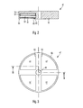
- a configuration of the detector 47 is illustrated as a sectional view in Figure 2 and as an elevational view in Figure 3 .
- the detector 47 comprises a ring-shaped carrier including an upper plate 55 having a central bore for providing the aperture 49 allowing the primary particle beam 13 and the secondary electrons 43 to pass through.
- Four semiconductor detectors are attached to a bottom surface of plate 55 such that a detection surface 59 of each semiconductor detector 57 is oriented towards the object plane 23.
- a membrane or window 61 is mounted in front of the detection surface 59 of each semiconductor detector 57.
- the membranes 61 have a function to at least partially prevent incidence of secondary electrons on the detection surfaces 59 of the semiconductor detectors 57.
- the membrane 61 is disposed at a small distance from the detection surface 59. It is, however, also possible that the membrane contacts or is directly attached as a membrane layer to the detection surface of the semiconductor detector and such that the membrane is carried by the semiconductor detector.
- the semiconductor detector can be a silicon drift detector, such as a detector obtainable under the product name Xflash® QUAD from Bruker AXS Microanalysis GmbH, Berlin, Germany.
- the membranes 61 can be configured such that they are not fixedly attached to the semiconductor detector or the ring structure such that they can be readily removed and replaced by other membranes.
- the exemplary embodiment shown in Figures 2 and 3 has axial projections 63 provided on the plate 55.
- the projections 63 include radially extending portions 65 adapted to carry the membranes 61 such that they are mounted on the detector 47.
- the membranes 61 can be clamped between the radial projections 65 and an outer axial ring-shaped projection 66 provided on the plate 55.
- the X-ray detector 57 comprises four separate semiconductor detectors 57 arranged in a configuration of four quadrants distributed around the aperture 49.
- the four semiconductor detectors 57 each have a same configuration and same properties, and detection signals of the four semiconductor detectors 57 are separately received by the controller 39.
- the detection surface of the detector is ring-shaped, traversed by the primary beam and located close to the location 21 of incidence of the particle beam 13 on the surface of the object 45. It is, however, possible to use other configurations of the detector.
- a detection surface of a detector can be located close to the location 21 without surrounding the electron beam 13.
- the detector may have plural separate detection surfaces which are located close to the location 21 for detecting electrons and X-rays. Different membranes can be arranged in front of the plural detection surfaces in order to change the detection efficiency for electrons relative to a detection efficiency for X-rays of a respective detector.
- the different detection surfaces may cover different amounts of solid angle relative to the location 21, such that an analysis of the detection signals of the different detectors allows to determine a three-dimensional structure of the sample.
- the four detectors 57 may all have same detection properties for electrons and X-rays. They will then differ by the fact that they cover different solid angles relative to the location 21 on the sample. The detectors will detect signals depending on an orientation of the surface of the sample at the location 21. Detection signals of the detectors may then be used to determine the three-dimensional structure of the sample. Background information relating to such determination of the three-dimensional structure can be obtained from the article " Three-Dimensional Characterization of Microstructures in a SEM", Wlodzimierz Drzazga et al., Meas. Sci. Technol. 17 (2006), pages 28-31 .
- the four membranes 61 arranged in front of the detection surfaces 59 of the four semiconductor detectors have different properties. Two different types of membranes are provided. Two membranes which are indicated by reference numeral 61 in Figure 3 have a transmittance for secondary electrons which is greater than a transmittance for secondary electrons of the two other membranes which are indicated in Figure 3 with reference numeral 61'.
- the two different types of membranes having different transmittances for secondary electrons are provided to modify a detection efficiency for secondary electrons of the detector.
- the membranes 61 can be made of a material including elements having a low atomic number such that a transmittance for X-rays is high. All membranes can be made from the same material and have different thicknesses for providing the different transmittances for secondary electrons.
- the membranes can be made of polyester, for example. Examples of suitable polyesters include terephtalat-polyester, such as polyethylenterephtalat-polyester. Suitable membranes can be obtained from the company DuPont, Wilmington, USA under the product name Mylar. Suitable thicknesses of the membranes can be, for example, within a range from 0.1 ⁇ m to 50 ⁇ m, and in particular from 1.0 ⁇ m to 10 ⁇ m. Other suitable membranes can be obtained from the company MoxTek, Orem, USA under the product name AP3.3. Still further membranes can be made of beryllium, for example.
- a membrane having the greater transmittance for electrons is provided by a foil having a thickness of 1 ⁇ m made of the material AP3.3, and a membrane having a lower transmittance for electrons is made of a foil of a thickness of 6 ⁇ m of the material Mylar.
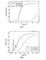
- Figure 4 shows a graph representing transmittances for electrons in dependence on the kinetic energy of the electrons for the two membranes obtained by numerical simulation.
- Figure 5 shows a graph representing transmittances for X-rays in dependence on kinetic energy of the electrons for the two membranes obtained by numerical simulation.
- a membrane having the greater transmittance for electrons is provided by a foil of a thickness of 1 ⁇ m of Mylar material, and a membrane having the smaller transmittance for electrons is provided by a foil having a thickness of 6 ⁇ m of the same Mylar material.
- FIG. 6 shows graphs representing count rates measured in an experiment using the detectors 47 of the particle beam system 1 shown in Figure 1 .
- the primary particle beam is directed onto a sample made of manganese (Mn).
- the graphs shown in Figure 6 illustrate a number of detection events recorded in a given time by the semiconductor detector having the thin foil located in front of it and a number of detection events recorded at the given time by the semiconductor detector having the thick foil located in front of it.
- Each graph is plotted in dependence on a kinetic energy of primary particles incident on the sample.
- Figure 7 shows a result of such analysis of the spectrum of the thin membrane shown in figure 6 .
- the full line of figure 7 shows the X-ray spectrum, and the broken line in figure 7 shows the backscattered electron spectrum.
- the X-ray spectrum can be further analyzed to determine chemical elements for which the spectrum is indicative.
- Background information relating to analyzing X-ray spectra with respect to elemental compositions of samples can be obtained from chapter 10.1 and 10.2 of L. Reimer, "Scanning Electron Microscopy", Second Edition, Springer 1998 .
- each energy spectrum will contain signal components related to electrons and signal components related to X-rays.
- the energy spectrum can be analyzed for each location to obtain the BSE signal and to generate and display an electron microscopic image of the sample based on the BSE signals of the plural locations.
- the signal component related to X-rays can be obtained from the recorded energy spectra for each location.
- An elemental composition can be determined from the signal component related to X-rays.
- Information on the chemical composition at the plural locations can be used to produce a map of the chemical composition of the sample.
- Such map can be displayed on a display medium, such as a monitor, as a color representation, wherein different colors represent different chemical elements. It is also possible to display the map of the chemical composition in superposition with the electron microscopic image. If the detector has plural detection surfaces covering different solid angles about the location 21 of incidence of the primary beam, it is also possible to determine a three-dimensional surface structure of the sample from the different signal components of the plural detection surfaces. The three-dimensional structure can be also shown on the display medium, wherein it is possible to colorize the display of the three-dimensional structure according to the elemental composition.
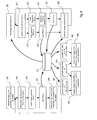
- the method comprises determining a scan strategy according to which a surface of a sample is scanned with a focused particle beam.
- the focused beam can be scanned along a meander shaped path and it can be scanned line by line, for example.
- a starting value of a location on the sample at which the scanning starts is determine in an initial step 101.
- the location can be determined based on coordinates x, y on the sample or based on any other suitable coordinate system.
- plural steps 103, 105 and 107 are repeatedly performed until a next location is determined in a step 109, wherein the steps 103, 105 and 107 will be again performed for the next location.
- the step 109 may also include termination of the repeated performance of steps 103, 105, 107 and 109, if the scanning of the sample is completed.
- the focused particle beam is directed to the location x, y on the sample.
- an energy spectrum S(x,y) associated with this location is recorded by reading detection signals of the detector.
- the energy spectrum S(x,y) will contain signal components related to electrons emanating from the locations O(x,y) and signal components related to X-rays emanating from the location O(x,y).
- the recorded spectrum S(x,y) is stored on a storage medium 111, such as a computer disk drive.
- the stored spectra are analyzed after completion of the scanning according to steps 101 to 109, or during such scanning.
- a computer reads a first spectrum in a step 201 and subsequent spectra in a step 209, in order to analyze the read spectra in steps 211 to 221 until all spectra recorded in the scanning are analyzed.
- the energy spectrum is analyzed in the step 211 in order to determine the signal components contained in the spectrum.
- the signal component related to backscattered electrons is extracted from the energy spectrum in a step 213, and a signal component related to X-rays is extracted from the energy spectrum in a step 217.
- Step 213 further includes integrating the signal component related to backscattered electrons to determine a BSE-value associated with the location O(x,y).
- This BSE-value BSE(x,y) is stored on the storage medium 111 in a step 215.
- the signal component R(x,y) related to X-ray is analyzed in step 219 in order to determine amounts C i of chemical elements at the location O(x,y).
- the determined amounts C i (x,y) are stored on the storage medium 111 in step 221.
- the procedure of recording of the spectra in the steps 101 to 109 and the procedure of analyzing the spectra in the steps 201 to 221 are independently performed in the flow chart shown in figure 8 . It is, however, also possible to transmit the spectra recorded in step 105 directly to the analyzing step 211 without storing in the storage medium 111.
- a step 303 an image is generated from the values C i (x,y), wherein this image represents a distribution of chemical elements in the sample.
- the images generated in steps 301 and 303 can be displayed on the display 81 ( figure 1 ) of the particle beam system. It is further possible to superimpose the images generated in steps 301 and 303 to form a common image in a step 305 and to display such image on display 81. This can be achieved by associating different colors with different chemical elements i and representing the amounts C i as intensities of the different colors. Such generated color image can be superimposed with the grey scale image obtained from the values BSE(x,y).
- the detector has plural detection surfaces covering different solid angles relative to the location of incidence of the particle beam, it is possible to determine the three-dimensional structure of the sample in a step 307.
- An image of the three-dimensional structure of the sample is superimposed with the chemical composition of the sample in a step 309. Again, this can be achieved by associating different colors with different chemical elements and colorizing the three-dimensional image according to these colors.
- Embodiments of the inspection method and system allows for a simultaneous detection of backscattered electrons and X-rays generated by the incident focused particle beam.
- the signal components related to backscattered electrons and the signal components related to X-rays can be associated with a same location on the sample defined by the location of incidence of the primary particle beam.
- the backscattered electrons typically emanate from a volume around this location which is smaller than a volume from which the X-rays emanate. This is a reason why BSE images generally have a better spatial resolution than EDX images. According to the present embodiments it is, however, possible to improve a spatial resolution of detected EDX images based on structure information obtained from the BSE images.
- a sample made of a first chemical element includes a narrow band formed of a second chemical element wherein a width of the narrow band is smaller than the spatial resolution of the EDX image but greater than the spatial resolution of the BSE image
- a detection signal related to the second chemical element can originate only from the narrow band having a width determined from the BSE image. This information can be used to improve the EDX image such that a width of the narrow band corresponding to the second chemical element as displayed in the image as reduced.
- the X-rays emanate from a larger volume of the sample than the backscattered electrons, it is also possible to detect defects in the sample which are located below the surface of the sample and which would not be detected using only backscattered electrons. It is further possible to identify, by analyzing the BSE image, a region of the sample where a defect is potentially present, and to verify the presence of such defect by analyzing the corresponding X-ray spectra associated with that region.
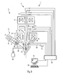
- FIG 9 is a schematic illustration of a particle beam apparatus 71 which can be used in a method of manufacture of an object.
- the particle beam apparatus 71 comprises a particle beam system 1 having a configuration similar to the particle beam system shown in figure 1 .
- the particle beam system 1 comprises a particle beam source 5 generating a particle beam 13 which can be focused at a location 21 via lenses 11, 29.
- the particle beam apparatus 71 further comprises a second particle beam system 73 configured to focus a second particle beam 75 also at location 21.
- the particle beam system 73 is an ion beam system comprising an ion source 77 and electrodes 79 for shaping and accelerating the ion beam 75, and beam deflectors 81 and focusing coils or focusing electrodes 83 for focusing the ion beam 75 at the location 21 and to scan the beam across a region about location 21.
- the particle beams 75 and 13 will be incident under different angles of incidence on a common region of the sample 21 and can be scanned across this regions by controlling the deflectors 81 and 41, respectively.
- An angle between the directions of the particle beams 75, 13 can be 45°, for example. Examples of conventional systems providing two particle beams are disclosed in US 2005/0184251 A1 and US 6,855,938 , the full disclosure of which is incorporated herein by reference.
- the particle beam apparatus illustrated with reference to figure 9 can be used in a method in which a thin plate or lamella 22 is manufactured from a sample 21 using the particle beam 75.
- the thin material plate or lamella 22 can be used as a sample in a subsequent inspection using a transmission electron microscope.
- the lamella should have a thickness of less than 1000 nm or less than 500 nm or even less than 200 nm.
- Conventional methods of manufacturing such thin material plates or lamellas are known from WO 2008/051937 A2 and WO 2008/051880 A2 , the full disclosure of which is incorporated herein by reference.
- the thin lamella 22 is manufactured by etching from the bulk material of the sample 25.
- the etching comprises supplying a reactive gas from a reservoir 84 via a supply pipe 85 towards the lamella 22.
- the reactive gas is activated by the ion beam 75 close to the lamella, and reacts with the sample 22 in a region close to the location of incidence of the ion beam 75 on the sample 22. Due to such reaction, material of the sample is released from the sample and can be removed via a vacuum system of the particle beam apparatus. Accordingly, it is possible to remove material from selected regions of the sample by operating the ion beam system 73 and supplying reactive gas via the supply pipe 85.
- Such process can be observed using the particle beam system 1 by obtaining an electron microscopic image of the lamella 22 under preparation, wherein such electron microscopic image can be continuously recorded or can be recorded after a predefined number of etching steps.
- the particle beam system 1 is used as an imaging tool.
- a thickness of the lamella under preparation can be determined based on detection signal components related to backscattered electrons and detection signal components related to X-rays.
- the particle beam 13 is directed to a location on the surface of the lamella.
- An intensity of the generated backscattered electrons is indicative of a thickness of the lamella since particles of the beam which are incident on and traverse a relatively thicker portion of the lamella will generate a greater amount of backscattered electrons than the particle beam incident on and traversing a relatively thinner portion of the lamella.
- the amount of backscattered electrons depends not only on the thickness of the lamella but also on the chemical composition of the lamella since different chemical elements produce different amounts of backscattered electrons upon irradiation with the particle beam 13.
- the chemical composition of the lamella at the location of incidence of the particle beam 13 can be determined by analyzing the detection signal components related to X-rays.
- the particle beam onto a location on the surface of the lamella and to determine the chemical composition of the lamella at the location of incidence of the particle beam on the sample based on the analysis of the signal components related to X-rays.
- the information on the chemical composition can be used in an analysis of the intensity of the backscattered electrons to finally determine the thickness of the lamella at the location of incidence of the beam 13. Based on the determined thickness of the lamella it is then possible to decide whether the particle beam system 73 should be operated to further remove material from that location or not.
- the chemical composition of the lamella may vary from location to location, it is possible to determine a thickness of the lamella at all locations with a relatively high accuracy since the chemical composition is taken into account.
- the removal of material is controlled based on detected electron intensities and detected X-ray intensities.
- a detector as illustrated with reference to figures 1 to 7 above can be used to obtain the detected electron intensities and the detected X-ray intensities.
- Such detector is shown at 47 in figure 9 , wherein the particle beam apparatus 71 further comprises a plate 89 which can be laterally displaced by an actuator as indicated by an arrow 91. Such that the plate 89 can be selectively positioned as shown in figure 9 and in a position in front of detector 47. In the position in front of the detector 47 the plate 89 covers the detector 47 when seen from a location 22 of incidence of the particle beam 75.
- the plate 89 then prevents small particles released from the sample due to the operation of the particle beam system 73 from being incident on and damaging the detector 49.
- the detector 47 is used to detect both electron intensities and X-ray intensities. It is, however, also possible to use separate detectors, i. e. an electron detector optimized for detecting electrons and substantially not detecting X-rays, and a separate X-ray detector optimized for detecting X-rays and substantially not detecting electrons.
- the particle beam apparatus illustrated with reference to figure 9 above uses separate particle beam systems for removing material and for observing the material removal. It is, however, also possible to perform the material removal using other systems using other methods than the combination of a focused ion beam and the supply of a reactive gas, wherein the apparatus performing the material removal can be separate from the apparatus performing the imaging for monitoring the material removal wherein the sample can be transported back and forth between the apparatus for removal and the apparatus for imaging.
Landscapes
- Chemical & Material Sciences (AREA)
- Analytical Chemistry (AREA)
- Engineering & Computer Science (AREA)
- Computer Vision & Pattern Recognition (AREA)
- Physics & Mathematics (AREA)
- Health & Medical Sciences (AREA)
- Life Sciences & Earth Sciences (AREA)
- Biochemistry (AREA)
- General Health & Medical Sciences (AREA)
- General Physics & Mathematics (AREA)
- Immunology (AREA)
- Pathology (AREA)
- Analysing Materials By The Use Of Radiation (AREA)
Applications Claiming Priority (1)
| Application Number | Priority Date | Filing Date | Title |
|---|---|---|---|
| DE102009036701A DE102009036701A1 (de) | 2009-08-07 | 2009-08-07 | Teilchenstrahlsystem und Untersuchungsverfahren hierzu |
Publications (3)
| Publication Number | Publication Date |
|---|---|
| EP2282197A2 true EP2282197A2 (fr) | 2011-02-09 |
| EP2282197A3 EP2282197A3 (fr) | 2012-01-04 |
| EP2282197B1 EP2282197B1 (fr) | 2020-06-17 |
Family
ID=43334757
Family Applications (1)
| Application Number | Title | Priority Date | Filing Date |
|---|---|---|---|
| EP10008253.6A Active EP2282197B1 (fr) | 2009-08-07 | 2010-08-06 | Systèmes et procédés de faisceau à particules |
Country Status (5)
| Country | Link |
|---|---|
| US (1) | US8450215B2 (fr) |
| EP (1) | EP2282197B1 (fr) |
| JP (1) | JP5584551B2 (fr) |
| CN (1) | CN102072913B (fr) |
| DE (1) | DE102009036701A1 (fr) |
Cited By (7)
| Publication number | Priority date | Publication date | Assignee | Title |
|---|---|---|---|---|
| DE102011080341A1 (de) | 2011-08-03 | 2013-02-07 | Carl Zeiss Nts Gmbh | Verfahren und Teilchenstrahlgerät zur Erzeugung eines Bildes eines Objekts |
| EP2697815A4 (fr) * | 2011-04-14 | 2014-09-10 | Coxem Co Ltd | Appareil combiné de microscope électronique à balayage et de spectroscopie des rayons x à dispersion d'énergie |
| WO2014202608A1 (fr) * | 2013-06-18 | 2014-12-24 | Bruker Nano Gmbh | Procédé de détection de rayons x ainsi que dispositif |
| EP2835817A1 (fr) * | 2013-08-09 | 2015-02-11 | Carl Zeiss Microscopy Ltd. | Procédé et système d'analyse de données pour l'analyse semi-automatique de particules au moyen d'un faisceau de particules chargées |
| EP3614414A1 (fr) * | 2018-08-20 | 2020-02-26 | FEI Company | Procédé d'examen d'un échantillon à l'aide d'un microscope à particules chargées |
| EP3648137A1 (fr) * | 2018-11-05 | 2020-05-06 | Jeol Ltd. | Microscope électronique et procédé de traitement d'image |
| GB2621003A (en) * | 2023-01-13 | 2024-01-31 | Oxford Instruments Nanotechnology Tools Ltd | Live chemical imaging with multiple detectors |
Families Citing this family (26)
| Publication number | Priority date | Publication date | Assignee | Title |
|---|---|---|---|---|
| JP5328264B2 (ja) * | 2008-08-21 | 2013-10-30 | 株式会社日立ハイテクサイエンス | 元素マッピング装置及び元素マッピング画像表示方法 |
| DE102009008063A1 (de) * | 2009-02-09 | 2010-08-19 | Carl Zeiss Nts Gmbh | Teilchenstrahlsystem |
| US8487252B2 (en) * | 2010-09-29 | 2013-07-16 | Carl Zeiss Nts Gmbh | Particle beam microscope and method for operating the particle beam microscope |
| DE102010056321B9 (de) * | 2010-12-27 | 2018-03-22 | Carl Zeiss Microscopy Gmbh | Partikelstrahlmikroskop |
| EP2544025A1 (fr) * | 2011-07-07 | 2013-01-09 | FEI Company | Détecteur au silicium à diffusion pour une utilisation dans un appareil de particules chargées |
| EP2605005A1 (fr) * | 2011-12-14 | 2013-06-19 | FEI Company | Groupage de données multimodales |
| JP2013033671A (ja) * | 2011-08-03 | 2013-02-14 | Hitachi High-Technologies Corp | 荷電粒子線装置 |
| MX2014003968A (es) * | 2011-10-14 | 2014-08-27 | Ingrain Inc | Metodo de imagen doble y sistema para generar una imagen multidimensional de una muestra. |
| US9153417B2 (en) | 2011-11-25 | 2015-10-06 | Totoltd. | Back scattered electron detector |
| JP5865676B2 (ja) * | 2011-11-25 | 2016-02-17 | 株式会社日立ハイテクノロジーズ | 荷電粒子線装置 |
| JP5951985B2 (ja) * | 2011-12-27 | 2016-07-13 | 株式会社ホロン | 円筒状原版検査装置および円筒状原版検査方法 |
| CN102592932A (zh) * | 2012-02-21 | 2012-07-18 | 南京特能电子有限公司 | 半导体背散射电子探测器 |
| JP6150991B2 (ja) | 2012-07-18 | 2017-06-21 | 株式会社日立ハイテクノロジーズ | 電子ビーム照射装置 |
| CN103344789B (zh) * | 2013-07-05 | 2015-09-09 | 北京工业大学 | 扫描电镜薄样品透射过滤-反射接收式衬度分离成像方法 |
| WO2017023574A1 (fr) * | 2015-07-31 | 2017-02-09 | Pulsetor, Llc | Détecteur segmenté destiné à un dispositif à faisceau de particules chargées |
| JP6174188B2 (ja) * | 2016-04-15 | 2017-08-02 | 株式会社ホロン | 円筒状原版検査装置および円筒状原版検査方法 |
| DE102016215419A1 (de) | 2016-08-17 | 2018-02-22 | Fraunhofer-Gesellschaft zur Förderung der angewandten Forschung e.V. | Messanordnung und Verfahren zum Lenken und Detektieren von Partikeln |
| JP6749189B2 (ja) * | 2016-09-16 | 2020-09-02 | キオクシア株式会社 | 組成分析方法および組成分析システム |
| JP7083629B2 (ja) * | 2017-11-27 | 2022-06-13 | 日本電子株式会社 | 定量分析方法および電子顕微鏡 |
| DE102018204683B3 (de) * | 2018-03-27 | 2019-08-08 | Carl Zeiss Microscopy Gmbh | Elektronenstrahlmikroskop |
| JP7085258B2 (ja) * | 2018-04-13 | 2022-06-16 | 株式会社ホロン | 超高速電子検出器および該検出器を組み込んだ走査型電子ビーム検査装置 |
| LU100806B1 (en) * | 2018-05-30 | 2019-12-02 | Luxembourg Inst Science & Tech List | Joint nanoscale three-dimensional imaging and chemical analysis |
| DE102019126200A1 (de) * | 2019-09-27 | 2021-04-01 | Carl Zeiss Microscopy Gmbh | EDX-Verfahren |
| DE102020102502A1 (de) * | 2020-01-31 | 2021-08-05 | Carl Zeiss Microscopy Gmbh | Verfahren, Teilchenstrahlsystem und Computerprogrammprodukt zur energiedispersiven Röntgenspektroskopie |
| US11577320B2 (en) * | 2020-06-15 | 2023-02-14 | Thermo Electron Scientific Instruments Llc | Shutter assembly for x-ray detection |
| WO2022122322A1 (fr) * | 2020-12-08 | 2022-06-16 | Asml Netherlands B.V. | Appareil et procédé permettant de diriger un faisceau de particules chargées vers un échantillon |
Citations (5)
| Publication number | Priority date | Publication date | Assignee | Title |
|---|---|---|---|---|
| US6855938B2 (en) | 2002-07-19 | 2005-02-15 | Carl Zeiss Nts Gmbh | Objective lens for an electron microscopy system and electron microscopy system |
| US20050184251A1 (en) | 2004-02-24 | 2005-08-25 | Masamichi Oi | FIB-SEM complex apparatus |
| US20060138325A1 (en) | 2004-12-29 | 2006-06-29 | Kyung-Duk Choi | X-ray detecting devices and apparatus for analyzing a sample using the same |
| WO2008051937A2 (fr) | 2006-10-20 | 2008-05-02 | Fei Company | Procédé pour créer un échantillon s/tem, et structure d'échantillon |
| WO2008051880A2 (fr) | 2006-10-20 | 2008-05-02 | Fei Company | Procédé et appareil pour extraire un échantillon, et le manipuler |
Family Cites Families (33)
| Publication number | Priority date | Publication date | Assignee | Title |
|---|---|---|---|---|
| NL231278A (fr) | 1957-09-26 | |||
| US3030512A (en) | 1958-11-21 | 1962-04-17 | Gen Electric | Monochromator system |
| US3100261A (en) | 1960-07-29 | 1963-08-06 | Gen Electric | X-ray analyzing apparatus wherein two comparative detector channels have different absorption versus frequency characteristics |
| US3204095A (en) | 1960-12-21 | 1965-08-31 | Hitachi Ltd | Electron probe microanalyzer with means to eliminate the effect of surface irregularities |
| JPS56153656A (en) | 1980-04-28 | 1981-11-27 | Hitachi Ltd | Electron microscope equipped with x-ray analyzing device |
| CA1170375A (fr) | 1980-06-11 | 1984-07-03 | Alan F. Reid | Methode et dispositif d'analyse de matieres |
| JPS5769655A (en) | 1980-10-16 | 1982-04-28 | Jeol Ltd | Electron beam device |
| JP2738761B2 (ja) | 1990-01-23 | 1998-04-08 | 日本電信電話株式会社 | X線計数管 |
| JP2637871B2 (ja) | 1991-12-26 | 1997-08-06 | 日本電信電話株式会社 | X線計数管 |
| JP3119959B2 (ja) * | 1993-02-05 | 2000-12-25 | セイコーインスツルメンツ株式会社 | 集束イオンビーム装置および加工観察装置 |
| GB2295454B (en) | 1994-11-25 | 1997-01-08 | Hitachi Ltd | Energy dispersive x-ray analyzer |
| US5903004A (en) | 1994-11-25 | 1999-05-11 | Hitachi, Ltd. | Energy dispersive X-ray analyzer |
| US5943388A (en) * | 1996-07-30 | 1999-08-24 | Nova R & D, Inc. | Radiation detector and non-destructive inspection |
| US5900667A (en) | 1996-10-04 | 1999-05-04 | Etec Systems, Inc. | Operating a solid state particle detector within a magnetic deflection field so as to minimize eddy currents |
| US5847388A (en) | 1997-06-11 | 1998-12-08 | Noran Instruments, Inc. | Collimator for high takeoff angle energy dispersive spectroscopy (EDS) detectors |
| JP3688160B2 (ja) * | 1999-09-17 | 2005-08-24 | 株式会社日立製作所 | 走査電子顕微鏡 |
| JP2002042713A (ja) | 2000-07-28 | 2002-02-08 | Jeol Ltd | 対物レンズ内検出器を備えた走査電子顕微鏡 |
| JP2002221504A (ja) * | 2001-01-26 | 2002-08-09 | Hitachi Ltd | X線検出装置および荷電粒子線装置 |
| JP3820964B2 (ja) * | 2001-11-13 | 2006-09-13 | 株式会社日立製作所 | 電子線を用いた試料観察装置および方法 |
| JP3909669B2 (ja) | 2002-01-29 | 2007-04-25 | 株式会社トプコンテクノハウス | 分析電子顕微鏡 |
| US20050103272A1 (en) * | 2002-02-25 | 2005-05-19 | Leo Elektronenmikroskopie Gmbh | Material processing system and method |
| US6843927B2 (en) * | 2002-08-27 | 2005-01-18 | Kla-Tencor Technologies Corporation | Method and apparatus for endpoint detection in electron beam assisted etching |
| JP4318962B2 (ja) * | 2003-06-02 | 2009-08-26 | エスアイアイ・ナノテクノロジー株式会社 | 薄膜加工における膜厚制御方法とそれを実行するシステム |
| US20070228287A1 (en) | 2006-03-20 | 2007-10-04 | Alis Technology Corporation | Systems and methods for a gas field ionization source |
| US7601953B2 (en) | 2006-03-20 | 2009-10-13 | Alis Corporation | Systems and methods for a gas field ion microscope |
| JP4497889B2 (ja) * | 2003-10-29 | 2010-07-07 | アルバック・ファイ株式会社 | 電子分光分析方法及び分析装置 |
| US7330535B2 (en) | 2005-11-10 | 2008-02-12 | General Electric Company | X-ray flux management device |
| DE102005061663B4 (de) | 2005-12-22 | 2008-07-17 | RUHR-UNIVERSITäT BOCHUM | Ionenimplantationsvorrichtung |
| US7851755B2 (en) * | 2006-12-20 | 2010-12-14 | Jeol Ltd. | Apparatus for detecting backscattered electrons in a beam apparatus |
| GB0712052D0 (en) * | 2007-06-21 | 2007-08-01 | Oxford Instr Molecular Biotool | Method for quantitive analysis of a material |
| EP2105944A1 (fr) | 2008-03-28 | 2009-09-30 | FEI Company | "Cellule environnementale" pour appareil optique à particules chargées |
| DE102009008063A1 (de) * | 2009-02-09 | 2010-08-19 | Carl Zeiss Nts Gmbh | Teilchenstrahlsystem |
| DE102009024928B4 (de) * | 2009-04-06 | 2012-07-12 | Bruker Nano Gmbh | Detektor, Vorrichtung und Verfahren zur gleichzeitigen, energiedispersiven Aufnahme von Rückstreuelektronen und Röntgenquanten |
-
2009
- 2009-08-07 DE DE102009036701A patent/DE102009036701A1/de not_active Ceased
-
2010
- 2010-08-05 US US12/806,111 patent/US8450215B2/en active Active
- 2010-08-06 EP EP10008253.6A patent/EP2282197B1/fr active Active
- 2010-08-06 JP JP2010178163A patent/JP5584551B2/ja active Active
- 2010-08-09 CN CN201010529590.9A patent/CN102072913B/zh active Active
Patent Citations (5)
| Publication number | Priority date | Publication date | Assignee | Title |
|---|---|---|---|---|
| US6855938B2 (en) | 2002-07-19 | 2005-02-15 | Carl Zeiss Nts Gmbh | Objective lens for an electron microscopy system and electron microscopy system |
| US20050184251A1 (en) | 2004-02-24 | 2005-08-25 | Masamichi Oi | FIB-SEM complex apparatus |
| US20060138325A1 (en) | 2004-12-29 | 2006-06-29 | Kyung-Duk Choi | X-ray detecting devices and apparatus for analyzing a sample using the same |
| WO2008051937A2 (fr) | 2006-10-20 | 2008-05-02 | Fei Company | Procédé pour créer un échantillon s/tem, et structure d'échantillon |
| WO2008051880A2 (fr) | 2006-10-20 | 2008-05-02 | Fei Company | Procédé et appareil pour extraire un échantillon, et le manipuler |
Non-Patent Citations (2)
| Title |
|---|
| L. REIMER: "Scanning Electron Microscopy, Second Edition", 1998, SPRINGER |
| WLODZIMIERZ DRZAZGA ET AL.: "Three-Dimensional Characterization of Microstructures in a SEM", MEAS. SCI. TECHNOL., vol. 17, 2006, pages 28 - 31, XP020103337, DOI: doi:10.1088/0957-0233/17/1/006 |
Cited By (14)
| Publication number | Priority date | Publication date | Assignee | Title |
|---|---|---|---|---|
| EP2697815A4 (fr) * | 2011-04-14 | 2014-09-10 | Coxem Co Ltd | Appareil combiné de microscope électronique à balayage et de spectroscopie des rayons x à dispersion d'énergie |
| DE102011080341A1 (de) | 2011-08-03 | 2013-02-07 | Carl Zeiss Nts Gmbh | Verfahren und Teilchenstrahlgerät zur Erzeugung eines Bildes eines Objekts |
| WO2014202608A1 (fr) * | 2013-06-18 | 2014-12-24 | Bruker Nano Gmbh | Procédé de détection de rayons x ainsi que dispositif |
| EP3011582B1 (fr) * | 2013-06-18 | 2021-03-03 | Bruker Nano GmbH | Procédé de détection de rayons x ainsi que dispositif |
| EP2835817A1 (fr) * | 2013-08-09 | 2015-02-11 | Carl Zeiss Microscopy Ltd. | Procédé et système d'analyse de données pour l'analyse semi-automatique de particules au moyen d'un faisceau de particules chargées |
| EP2881972A1 (fr) * | 2013-08-09 | 2015-06-10 | Carl Zeiss Microscopy Ltd. | Procédé et système d'analyse de données pour l'analyse semi-automatique de particules au moyen d'un faisceau de particules chargées |
| US10955368B2 (en) | 2013-08-09 | 2021-03-23 | Carl Zeiss Microscopy Ltd. | Method and data analysis system for semi-automated particle analysis using a charged particle beam |
| US11002692B2 (en) | 2018-08-20 | 2021-05-11 | Fei Company | Method of examining a sample using a charged particle microscope |
| EP3614414A1 (fr) * | 2018-08-20 | 2020-02-26 | FEI Company | Procédé d'examen d'un échantillon à l'aide d'un microscope à particules chargées |
| EP3648137A1 (fr) * | 2018-11-05 | 2020-05-06 | Jeol Ltd. | Microscope électronique et procédé de traitement d'image |
| US10957513B2 (en) | 2018-11-05 | 2021-03-23 | Jeol Ltd. | Electron microscope and image processing method |
| GB2621003A (en) * | 2023-01-13 | 2024-01-31 | Oxford Instruments Nanotechnology Tools Ltd | Live chemical imaging with multiple detectors |
| CN118348043A (zh) * | 2023-01-13 | 2024-07-16 | 牛津仪器纳米技术工具有限公司 | 多探测器实时化学成像 |
| GB2621003B (en) * | 2023-01-13 | 2024-09-04 | Oxford Instruments Nanotechnology Tools Ltd | Live chemical imaging with multiple detectors |
Also Published As
| Publication number | Publication date |
|---|---|
| DE102009036701A1 (de) | 2011-03-03 |
| US8450215B2 (en) | 2013-05-28 |
| DE102009036701A8 (de) | 2011-06-01 |
| US20110031215A1 (en) | 2011-02-10 |
| JP5584551B2 (ja) | 2014-09-03 |
| JP2011040384A (ja) | 2011-02-24 |
| CN102072913A (zh) | 2011-05-25 |
| EP2282197A3 (fr) | 2012-01-04 |
| CN102072913B (zh) | 2015-09-09 |
| EP2282197B1 (fr) | 2020-06-17 |
Similar Documents
| Publication | Publication Date | Title |
|---|---|---|
| EP2282197B1 (fr) | Systèmes et procédés de faisceau à particules | |
| EP2216798B1 (fr) | Système de faisceau à particules | |
| EP2387062B1 (fr) | Détection simultanée d'électrons | |
| US8624184B1 (en) | Methods for spatially resolved alignment of independent spectroscopic data from scanning transmission electron microscopes | |
| JP6751286B2 (ja) | 荷電粒子ビーム試料検査システムおよびその動作方法 | |
| US8093556B2 (en) | Device and method for analyzing a sample | |
| US20130292568A1 (en) | Scanning electron microscope and length measuring method using the same | |
| EP2365514A1 (fr) | Colonne de particules chargées de faisceau double et son procédé de contrôle | |
| US9535020B2 (en) | Analyzing an object using a particle beam apparatus | |
| US9620331B1 (en) | Method for analyzing an object and charged particle beam device for carrying out the method | |
| CN108538693B (zh) | 带电粒子显微镜的像差测量 | |
| KR102557373B1 (ko) | 집속 이온 빔 불순물 식별 | |
| US20240272099A1 (en) | High resolution, low energy electron microscope for providing topography information and method of mask inspection | |
| US9741525B1 (en) | Charged-particle microscope with astigmatism compensation and energy-selection | |
| EP2219204B1 (fr) | Agencement et procédé pour l'amélioration du contraste dans un dispositif à faisceau de particules chargées pour l'inspection d'un spécimen | |
| US20120326030A1 (en) | Particle Beam Microscope | |
| EP2698805A1 (fr) | Procédé de réalisation EDX dans un microscope à particules chargées | |
| GB2621003A (en) | Live chemical imaging with multiple detectors | |
| JP2005183881A (ja) | 荷電粒子ビームを用いた半導体ウェハ試料の検査方法および装置 | |
| KR20260053555A (ko) | 하전 입자 빔 장치 | |
| Inkson | The University of Sheffield, Sheffield, United Kingdom | |
| TE SG | 10* AAA SSSS _1 l– |
Legal Events
| Date | Code | Title | Description |
|---|---|---|---|
| PUAI | Public reference made under article 153(3) epc to a published international application that has entered the european phase |
Free format text: ORIGINAL CODE: 0009012 |
|
| AK | Designated contracting states |
Kind code of ref document: A2 Designated state(s): AL AT BE BG CH CY CZ DE DK EE ES FI FR GB GR HR HU IE IS IT LI LT LU LV MC MK MT NL NO PL PT RO SE SI SK SM TR |
|
| AX | Request for extension of the european patent |
Extension state: BA ME RS |
|
| RIC1 | Information provided on ipc code assigned before grant |
Ipc: H01J 37/28 20060101ALI20110909BHEP Ipc: H01J 37/244 20060101ALI20110909BHEP Ipc: G01N 23/225 20060101AFI20110909BHEP |
|
| PUAL | Search report despatched |
Free format text: ORIGINAL CODE: 0009013 |
|
| AK | Designated contracting states |
Kind code of ref document: A3 Designated state(s): AL AT BE BG CH CY CZ DE DK EE ES FI FR GB GR HR HU IE IS IT LI LT LU LV MC MK MT NL NO PL PT RO SE SI SK SM TR |
|
| AX | Request for extension of the european patent |
Extension state: BA ME RS |
|
| RIC1 | Information provided on ipc code assigned before grant |
Ipc: H01J 37/305 20060101ALI20111201BHEP Ipc: G01N 1/32 20060101ALI20111201BHEP Ipc: H01J 37/28 20060101ALI20111201BHEP Ipc: H01J 37/244 20060101ALI20111201BHEP Ipc: G01N 23/225 20060101AFI20111201BHEP |
|
| 17P | Request for examination filed |
Effective date: 20120702 |
|
| 17Q | First examination report despatched |
Effective date: 20120914 |
|
| STAA | Information on the status of an ep patent application or granted ep patent |
Free format text: STATUS: EXAMINATION IS IN PROGRESS |
|
| REG | Reference to a national code |
Ref country code: DE Ref legal event code: R079 Ref document number: 602010064616 Country of ref document: DE Free format text: PREVIOUS MAIN CLASS: G01N0023225000 Ipc: G01N0023225200 |
|
| GRAP | Despatch of communication of intention to grant a patent |
Free format text: ORIGINAL CODE: EPIDOSNIGR1 |
|
| STAA | Information on the status of an ep patent application or granted ep patent |
Free format text: STATUS: GRANT OF PATENT IS INTENDED |
|
| RIC1 | Information provided on ipc code assigned before grant |
Ipc: H01J 37/256 20060101ALI20191101BHEP Ipc: H01J 37/22 20060101ALI20191101BHEP Ipc: H01J 37/305 20060101ALI20191101BHEP Ipc: H01J 37/244 20060101ALI20191101BHEP Ipc: G01N 1/32 20060101ALI20191101BHEP Ipc: H01J 37/28 20060101ALI20191101BHEP Ipc: G01N 23/2252 20180101AFI20191101BHEP |
|
| INTG | Intention to grant announced |
Effective date: 20191204 |
|
| RAP1 | Party data changed (applicant data changed or rights of an application transferred) |
Owner name: CARL ZEISS MICROSCOPY GMBH |
|
| GRAS | Grant fee paid |
Free format text: ORIGINAL CODE: EPIDOSNIGR3 |
|
| GRAJ | Information related to disapproval of communication of intention to grant by the applicant or resumption of examination proceedings by the epo deleted |
Free format text: ORIGINAL CODE: EPIDOSDIGR1 |
|
| GRAL | Information related to payment of fee for publishing/printing deleted |
Free format text: ORIGINAL CODE: EPIDOSDIGR3 |
|
| STAA | Information on the status of an ep patent application or granted ep patent |
Free format text: STATUS: EXAMINATION IS IN PROGRESS |
|
| GRAR | Information related to intention to grant a patent recorded |
Free format text: ORIGINAL CODE: EPIDOSNIGR71 |
|
| STAA | Information on the status of an ep patent application or granted ep patent |
Free format text: STATUS: GRANT OF PATENT IS INTENDED |
|
| GRAA | (expected) grant |
Free format text: ORIGINAL CODE: 0009210 |
|
| STAA | Information on the status of an ep patent application or granted ep patent |
Free format text: STATUS: THE PATENT HAS BEEN GRANTED |
|
| INTC | Intention to grant announced (deleted) | ||
| AK | Designated contracting states |
Kind code of ref document: B1 Designated state(s): AL AT BE BG CH CY CZ DE DK EE ES FI FR GB GR HR HU IE IS IT LI LT LU LV MC MK MT NL NO PL PT RO SE SI SK SM TR |
|
| INTG | Intention to grant announced |
Effective date: 20200512 |
|
| REG | Reference to a national code |
Ref country code: GB Ref legal event code: FG4D |
|
| REG | Reference to a national code |
Ref country code: CH Ref legal event code: EP |
|
| REG | Reference to a national code |
Ref country code: IE Ref legal event code: FG4D |
|
| REG | Reference to a national code |
Ref country code: DE Ref legal event code: R096 Ref document number: 602010064616 Country of ref document: DE |
|
| REG | Reference to a national code |
Ref country code: AT Ref legal event code: REF Ref document number: 1281930 Country of ref document: AT Kind code of ref document: T Effective date: 20200715 |
|
| PG25 | Lapsed in a contracting state [announced via postgrant information from national office to epo] |
Ref country code: GR Free format text: LAPSE BECAUSE OF FAILURE TO SUBMIT A TRANSLATION OF THE DESCRIPTION OR TO PAY THE FEE WITHIN THE PRESCRIBED TIME-LIMIT Effective date: 20200918 Ref country code: LT Free format text: LAPSE BECAUSE OF FAILURE TO SUBMIT A TRANSLATION OF THE DESCRIPTION OR TO PAY THE FEE WITHIN THE PRESCRIBED TIME-LIMIT Effective date: 20200617 Ref country code: SE Free format text: LAPSE BECAUSE OF FAILURE TO SUBMIT A TRANSLATION OF THE DESCRIPTION OR TO PAY THE FEE WITHIN THE PRESCRIBED TIME-LIMIT Effective date: 20200617 Ref country code: FI Free format text: LAPSE BECAUSE OF FAILURE TO SUBMIT A TRANSLATION OF THE DESCRIPTION OR TO PAY THE FEE WITHIN THE PRESCRIBED TIME-LIMIT Effective date: 20200617 Ref country code: NO Free format text: LAPSE BECAUSE OF FAILURE TO SUBMIT A TRANSLATION OF THE DESCRIPTION OR TO PAY THE FEE WITHIN THE PRESCRIBED TIME-LIMIT Effective date: 20200917 |
|
| REG | Reference to a national code |
Ref country code: LT Ref legal event code: MG4D |
|
| REG | Reference to a national code |
Ref country code: NL Ref legal event code: MP Effective date: 20200617 |
|
| PG25 | Lapsed in a contracting state [announced via postgrant information from national office to epo] |
Ref country code: HR Free format text: LAPSE BECAUSE OF FAILURE TO SUBMIT A TRANSLATION OF THE DESCRIPTION OR TO PAY THE FEE WITHIN THE PRESCRIBED TIME-LIMIT Effective date: 20200617 Ref country code: LV Free format text: LAPSE BECAUSE OF FAILURE TO SUBMIT A TRANSLATION OF THE DESCRIPTION OR TO PAY THE FEE WITHIN THE PRESCRIBED TIME-LIMIT Effective date: 20200617 Ref country code: BG Free format text: LAPSE BECAUSE OF FAILURE TO SUBMIT A TRANSLATION OF THE DESCRIPTION OR TO PAY THE FEE WITHIN THE PRESCRIBED TIME-LIMIT Effective date: 20200917 |
|
| REG | Reference to a national code |
Ref country code: AT Ref legal event code: MK05 Ref document number: 1281930 Country of ref document: AT Kind code of ref document: T Effective date: 20200617 |
|
| PG25 | Lapsed in a contracting state [announced via postgrant information from national office to epo] |
Ref country code: NL Free format text: LAPSE BECAUSE OF FAILURE TO SUBMIT A TRANSLATION OF THE DESCRIPTION OR TO PAY THE FEE WITHIN THE PRESCRIBED TIME-LIMIT Effective date: 20200617 Ref country code: AL Free format text: LAPSE BECAUSE OF FAILURE TO SUBMIT A TRANSLATION OF THE DESCRIPTION OR TO PAY THE FEE WITHIN THE PRESCRIBED TIME-LIMIT Effective date: 20200617 |
|
| PG25 | Lapsed in a contracting state [announced via postgrant information from national office to epo] |
Ref country code: IT Free format text: LAPSE BECAUSE OF FAILURE TO SUBMIT A TRANSLATION OF THE DESCRIPTION OR TO PAY THE FEE WITHIN THE PRESCRIBED TIME-LIMIT Effective date: 20200617 Ref country code: RO Free format text: LAPSE BECAUSE OF FAILURE TO SUBMIT A TRANSLATION OF THE DESCRIPTION OR TO PAY THE FEE WITHIN THE PRESCRIBED TIME-LIMIT Effective date: 20200617 Ref country code: AT Free format text: LAPSE BECAUSE OF FAILURE TO SUBMIT A TRANSLATION OF THE DESCRIPTION OR TO PAY THE FEE WITHIN THE PRESCRIBED TIME-LIMIT Effective date: 20200617 Ref country code: CZ Free format text: LAPSE BECAUSE OF FAILURE TO SUBMIT A TRANSLATION OF THE DESCRIPTION OR TO PAY THE FEE WITHIN THE PRESCRIBED TIME-LIMIT Effective date: 20200617 Ref country code: EE Free format text: LAPSE BECAUSE OF FAILURE TO SUBMIT A TRANSLATION OF THE DESCRIPTION OR TO PAY THE FEE WITHIN THE PRESCRIBED TIME-LIMIT Effective date: 20200617 Ref country code: SM Free format text: LAPSE BECAUSE OF FAILURE TO SUBMIT A TRANSLATION OF THE DESCRIPTION OR TO PAY THE FEE WITHIN THE PRESCRIBED TIME-LIMIT Effective date: 20200617 Ref country code: ES Free format text: LAPSE BECAUSE OF FAILURE TO SUBMIT A TRANSLATION OF THE DESCRIPTION OR TO PAY THE FEE WITHIN THE PRESCRIBED TIME-LIMIT Effective date: 20200617 Ref country code: PT Free format text: LAPSE BECAUSE OF FAILURE TO SUBMIT A TRANSLATION OF THE DESCRIPTION OR TO PAY THE FEE WITHIN THE PRESCRIBED TIME-LIMIT Effective date: 20201019 |
|
| PG25 | Lapsed in a contracting state [announced via postgrant information from national office to epo] |
Ref country code: IS Free format text: LAPSE BECAUSE OF FAILURE TO SUBMIT A TRANSLATION OF THE DESCRIPTION OR TO PAY THE FEE WITHIN THE PRESCRIBED TIME-LIMIT Effective date: 20201017 Ref country code: PL Free format text: LAPSE BECAUSE OF FAILURE TO SUBMIT A TRANSLATION OF THE DESCRIPTION OR TO PAY THE FEE WITHIN THE PRESCRIBED TIME-LIMIT Effective date: 20200617 Ref country code: SK Free format text: LAPSE BECAUSE OF FAILURE TO SUBMIT A TRANSLATION OF THE DESCRIPTION OR TO PAY THE FEE WITHIN THE PRESCRIBED TIME-LIMIT Effective date: 20200617 |
|
| REG | Reference to a national code |
Ref country code: DE Ref legal event code: R097 Ref document number: 602010064616 Country of ref document: DE |
|
| PG25 | Lapsed in a contracting state [announced via postgrant information from national office to epo] |
Ref country code: MC Free format text: LAPSE BECAUSE OF FAILURE TO SUBMIT A TRANSLATION OF THE DESCRIPTION OR TO PAY THE FEE WITHIN THE PRESCRIBED TIME-LIMIT Effective date: 20200617 |
|
| REG | Reference to a national code |
Ref country code: CH Ref legal event code: PL |
|
| PLBE | No opposition filed within time limit |
Free format text: ORIGINAL CODE: 0009261 |
|
| STAA | Information on the status of an ep patent application or granted ep patent |
Free format text: STATUS: NO OPPOSITION FILED WITHIN TIME LIMIT |
|
| PG25 | Lapsed in a contracting state [announced via postgrant information from national office to epo] |
Ref country code: CH Free format text: LAPSE BECAUSE OF NON-PAYMENT OF DUE FEES Effective date: 20200831 Ref country code: DK Free format text: LAPSE BECAUSE OF FAILURE TO SUBMIT A TRANSLATION OF THE DESCRIPTION OR TO PAY THE FEE WITHIN THE PRESCRIBED TIME-LIMIT Effective date: 20200617 Ref country code: LI Free format text: LAPSE BECAUSE OF NON-PAYMENT OF DUE FEES Effective date: 20200831 Ref country code: LU Free format text: LAPSE BECAUSE OF NON-PAYMENT OF DUE FEES Effective date: 20200806 |
|
| 26N | No opposition filed |
Effective date: 20210318 |
|
| REG | Reference to a national code |
Ref country code: BE Ref legal event code: MM Effective date: 20200831 |
|
| PG25 | Lapsed in a contracting state [announced via postgrant information from national office to epo] |
Ref country code: SI Free format text: LAPSE BECAUSE OF FAILURE TO SUBMIT A TRANSLATION OF THE DESCRIPTION OR TO PAY THE FEE WITHIN THE PRESCRIBED TIME-LIMIT Effective date: 20200617 |
|
| PG25 | Lapsed in a contracting state [announced via postgrant information from national office to epo] |
Ref country code: FR Free format text: LAPSE BECAUSE OF NON-PAYMENT OF DUE FEES Effective date: 20200817 |
|
| PG25 | Lapsed in a contracting state [announced via postgrant information from national office to epo] |
Ref country code: IE Free format text: LAPSE BECAUSE OF NON-PAYMENT OF DUE FEES Effective date: 20200806 Ref country code: BE Free format text: LAPSE BECAUSE OF NON-PAYMENT OF DUE FEES Effective date: 20200831 |
|
| PG25 | Lapsed in a contracting state [announced via postgrant information from national office to epo] |
Ref country code: TR Free format text: LAPSE BECAUSE OF FAILURE TO SUBMIT A TRANSLATION OF THE DESCRIPTION OR TO PAY THE FEE WITHIN THE PRESCRIBED TIME-LIMIT Effective date: 20200617 Ref country code: MT Free format text: LAPSE BECAUSE OF FAILURE TO SUBMIT A TRANSLATION OF THE DESCRIPTION OR TO PAY THE FEE WITHIN THE PRESCRIBED TIME-LIMIT Effective date: 20200617 Ref country code: CY Free format text: LAPSE BECAUSE OF FAILURE TO SUBMIT A TRANSLATION OF THE DESCRIPTION OR TO PAY THE FEE WITHIN THE PRESCRIBED TIME-LIMIT Effective date: 20200617 |
|
| PG25 | Lapsed in a contracting state [announced via postgrant information from national office to epo] |
Ref country code: MK Free format text: LAPSE BECAUSE OF FAILURE TO SUBMIT A TRANSLATION OF THE DESCRIPTION OR TO PAY THE FEE WITHIN THE PRESCRIBED TIME-LIMIT Effective date: 20200617 |
|
| PGFP | Annual fee paid to national office [announced via postgrant information from national office to epo] |
Ref country code: DE Payment date: 20250820 Year of fee payment: 16 |
|
| PGFP | Annual fee paid to national office [announced via postgrant information from national office to epo] |
Ref country code: GB Payment date: 20250820 Year of fee payment: 16 |