EP2282377B1 - Elektrischer Steckverbinder mit verbesserter Übersprechungskompensation - Google Patents
Elektrischer Steckverbinder mit verbesserter Übersprechungskompensation Download PDFInfo
- Publication number
- EP2282377B1 EP2282377B1 EP10075635.2A EP10075635A EP2282377B1 EP 2282377 B1 EP2282377 B1 EP 2282377B1 EP 10075635 A EP10075635 A EP 10075635A EP 2282377 B1 EP2282377 B1 EP 2282377B1
- Authority
- EP
- European Patent Office
- Prior art keywords
- plug
- jack
- trace
- leg
- compensation
- Prior art date
- Legal status (The legal status is an assumption and is not a legal conclusion. Google has not performed a legal analysis and makes no representation as to the accuracy of the status listed.)
- Expired - Lifetime
Links
- 230000001976 improved effect Effects 0.000 title abstract description 9
- 230000008878 coupling Effects 0.000 claims abstract description 82
- 238000010168 coupling process Methods 0.000 claims abstract description 82
- 238000005859 coupling reaction Methods 0.000 claims abstract description 82
- 230000008859 change Effects 0.000 claims description 19
- 239000003990 capacitor Substances 0.000 claims description 6
- 230000010363 phase shift Effects 0.000 abstract description 17
- 230000003247 decreasing effect Effects 0.000 abstract description 4
- 239000013598 vector Substances 0.000 description 43
- 238000000034 method Methods 0.000 description 38
- 238000004891 communication Methods 0.000 description 32
- 230000001939 inductive effect Effects 0.000 description 23
- 238000013461 design Methods 0.000 description 22
- 239000000696 magnetic material Substances 0.000 description 17
- 238000010586 diagram Methods 0.000 description 16
- 239000000463 material Substances 0.000 description 13
- 239000004020 conductor Substances 0.000 description 12
- 230000000694 effects Effects 0.000 description 11
- 230000001965 increasing effect Effects 0.000 description 10
- 239000011162 core material Substances 0.000 description 9
- 229910000859 α-Fe Inorganic materials 0.000 description 8
- 238000012545 processing Methods 0.000 description 5
- UQSXHKLRYXJYBZ-UHFFFAOYSA-N Iron oxide Chemical compound [Fe]=O UQSXHKLRYXJYBZ-UHFFFAOYSA-N 0.000 description 4
- 238000006073 displacement reaction Methods 0.000 description 4
- 230000008569 process Effects 0.000 description 4
- SXZSFWHOSHAKMN-UHFFFAOYSA-N 2,3,4,4',5-Pentachlorobiphenyl Chemical compound C1=CC(Cl)=CC=C1C1=CC(Cl)=C(Cl)C(Cl)=C1Cl SXZSFWHOSHAKMN-UHFFFAOYSA-N 0.000 description 3
- 230000008901 benefit Effects 0.000 description 3
- 230000005540 biological transmission Effects 0.000 description 3
- 230000001419 dependent effect Effects 0.000 description 3
- 230000002441 reversible effect Effects 0.000 description 3
- 238000004804 winding Methods 0.000 description 3
- RYGMFSIKBFXOCR-UHFFFAOYSA-N Copper Chemical compound [Cu] RYGMFSIKBFXOCR-UHFFFAOYSA-N 0.000 description 2
- XEEYBQQBJWHFJM-UHFFFAOYSA-N Iron Chemical compound [Fe] XEEYBQQBJWHFJM-UHFFFAOYSA-N 0.000 description 2
- PXHVJJICTQNCMI-UHFFFAOYSA-N Nickel Chemical compound [Ni] PXHVJJICTQNCMI-UHFFFAOYSA-N 0.000 description 2
- 229910052802 copper Inorganic materials 0.000 description 2
- 239000010949 copper Substances 0.000 description 2
- 230000001934 delay Effects 0.000 description 2
- 230000002500 effect on skin Effects 0.000 description 2
- 230000004907 flux Effects 0.000 description 2
- 238000003780 insertion Methods 0.000 description 2
- 230000037431 insertion Effects 0.000 description 2
- 238000004519 manufacturing process Methods 0.000 description 2
- 238000012986 modification Methods 0.000 description 2
- 230000004048 modification Effects 0.000 description 2
- QELJHCBNGDEXLD-UHFFFAOYSA-N nickel zinc Chemical compound [Ni].[Zn] QELJHCBNGDEXLD-UHFFFAOYSA-N 0.000 description 2
- 230000035699 permeability Effects 0.000 description 2
- 239000004033 plastic Substances 0.000 description 2
- 230000004044 response Effects 0.000 description 2
- 238000012216 screening Methods 0.000 description 2
- CWYNVVGOOAEACU-UHFFFAOYSA-N Fe2+ Chemical compound [Fe+2] CWYNVVGOOAEACU-UHFFFAOYSA-N 0.000 description 1
- 239000004952 Polyamide Substances 0.000 description 1
- 229910000831 Steel Inorganic materials 0.000 description 1
- 239000002131 composite material Substances 0.000 description 1
- 150000001875 compounds Chemical class 0.000 description 1
- 238000010276 construction Methods 0.000 description 1
- 230000003111 delayed effect Effects 0.000 description 1
- 230000008021 deposition Effects 0.000 description 1
- 238000005530 etching Methods 0.000 description 1
- 238000007654 immersion Methods 0.000 description 1
- 230000006872 improvement Effects 0.000 description 1
- 238000009413 insulation Methods 0.000 description 1
- 239000012212 insulator Substances 0.000 description 1
- 230000003993 interaction Effects 0.000 description 1
- 229910052742 iron Inorganic materials 0.000 description 1
- WJZHMLNIAZSFDO-UHFFFAOYSA-N manganese zinc Chemical compound [Mn].[Zn] WJZHMLNIAZSFDO-UHFFFAOYSA-N 0.000 description 1
- 230000007246 mechanism Effects 0.000 description 1
- 239000002184 metal Substances 0.000 description 1
- 229910052751 metal Inorganic materials 0.000 description 1
- 150000002739 metals Chemical class 0.000 description 1
- 230000000116 mitigating effect Effects 0.000 description 1
- 239000000203 mixture Substances 0.000 description 1
- 229910052759 nickel Inorganic materials 0.000 description 1
- 229920002647 polyamide Polymers 0.000 description 1
- 150000003071 polychlorinated biphenyls Chemical class 0.000 description 1
- 229920006149 polyester-amide block copolymer Polymers 0.000 description 1
- 239000012256 powdered iron Substances 0.000 description 1
- 230000000630 rising effect Effects 0.000 description 1
- 239000004065 semiconductor Substances 0.000 description 1
- 238000000926 separation method Methods 0.000 description 1
- 238000004904 shortening Methods 0.000 description 1
- 238000005476 soldering Methods 0.000 description 1
- 239000007787 solid Substances 0.000 description 1
- 239000010959 steel Substances 0.000 description 1
- 239000000758 substrate Substances 0.000 description 1
- 238000003466 welding Methods 0.000 description 1
Images


Classifications
-
- H—ELECTRICITY
- H01—ELECTRIC ELEMENTS
- H01R—ELECTRICALLY-CONDUCTIVE CONNECTIONS; STRUCTURAL ASSOCIATIONS OF A PLURALITY OF MUTUALLY-INSULATED ELECTRICAL CONNECTING ELEMENTS; COUPLING DEVICES; CURRENT COLLECTORS
- H01R13/00—Details of coupling devices of the kinds covered by groups H01R12/70 or H01R24/00 - H01R33/00
- H01R13/646—Details of coupling devices of the kinds covered by groups H01R12/70 or H01R24/00 - H01R33/00 specially adapted for high-frequency, e.g. structures providing an impedance match or phase match
- H01R13/6461—Means for preventing cross-talk
- H01R13/6464—Means for preventing cross-talk by adding capacitive elements
- H01R13/6466—Means for preventing cross-talk by adding capacitive elements on substrates, e.g. printed circuit boards [PCB]
-
- H—ELECTRICITY
- H01—ELECTRIC ELEMENTS
- H01R—ELECTRICALLY-CONDUCTIVE CONNECTIONS; STRUCTURAL ASSOCIATIONS OF A PLURALITY OF MUTUALLY-INSULATED ELECTRICAL CONNECTING ELEMENTS; COUPLING DEVICES; CURRENT COLLECTORS
- H01R13/00—Details of coupling devices of the kinds covered by groups H01R12/70 or H01R24/00 - H01R33/00
- H01R13/66—Structural association with built-in electrical component
- H01R13/719—Structural association with built-in electrical component specially adapted for high frequency, e.g. with filters
-
- H—ELECTRICITY
- H01—ELECTRIC ELEMENTS
- H01R—ELECTRICALLY-CONDUCTIVE CONNECTIONS; STRUCTURAL ASSOCIATIONS OF A PLURALITY OF MUTUALLY-INSULATED ELECTRICAL CONNECTING ELEMENTS; COUPLING DEVICES; CURRENT COLLECTORS
- H01R24/00—Two-part coupling devices, or either of their cooperating parts, characterised by their overall structure
- H01R24/60—Contacts spaced along planar side wall transverse to longitudinal axis of engagement
- H01R24/62—Sliding engagements with one side only, e.g. modular jack coupling devices
- H01R24/64—Sliding engagements with one side only, e.g. modular jack coupling devices for high frequency, e.g. RJ 45
-
- H—ELECTRICITY
- H05—ELECTRIC TECHNIQUES NOT OTHERWISE PROVIDED FOR
- H05K—PRINTED CIRCUITS; CASINGS OR CONSTRUCTIONAL DETAILS OF ELECTRIC APPARATUS; MANUFACTURE OF ASSEMBLAGES OF ELECTRICAL COMPONENTS
- H05K1/00—Printed circuits
- H05K1/02—Details
- H05K1/0213—Electrical arrangements not otherwise provided for
- H05K1/0216—Reduction of cross-talk, noise or electromagnetic interference
- H05K1/0228—Compensation of cross-talk by a mutually correlated lay-out of printed circuit traces, e.g. for compensation of cross-talk in mounted connectors
-
- Y—GENERAL TAGGING OF NEW TECHNOLOGICAL DEVELOPMENTS; GENERAL TAGGING OF CROSS-SECTIONAL TECHNOLOGIES SPANNING OVER SEVERAL SECTIONS OF THE IPC; TECHNICAL SUBJECTS COVERED BY FORMER USPC CROSS-REFERENCE ART COLLECTIONS [XRACs] AND DIGESTS
- Y10—TECHNICAL SUBJECTS COVERED BY FORMER USPC
- Y10S—TECHNICAL SUBJECTS COVERED BY FORMER USPC CROSS-REFERENCE ART COLLECTIONS [XRACs] AND DIGESTS
- Y10S439/00—Electrical connectors
- Y10S439/941—Crosstalk suppression
Definitions
- the present invention relates generally to electrical connectors, and more particularly, to a modular communication jack design with crosstalk compensation that is less susceptible to propagation delay effects at high frequencies.
- the electrical connector is a modular jack that is adapted to receive a modular plug.
- a known amount of offending crosstalk A0 which is approximately canceled by the two or more stages of compensating crosstalk.
- compensating crosstalk A1 is introduced between the pairs, and it has a first predetermined magnitude and phase at a given frequency.
- compensating crosstalk A2 is introduced between the pairs, and it has a second predetermined magnitude and phase at the given frequency.
- Multiple compensation stages are needed because, at high frequencies, compensating crosstalk cannot be introduced that is exactly 180 degrees out of phase with the offending crosstalk because of propagation delay.
- the electrical connector is constructed using a multi-layer printed wiring board having input and output terminals where connection to metallic wires is made. These terminals are interconnected on the printed wiring board by metallic paths that are arranged to provide multiple stages of compensating crosstalk.
- the near-end crosstalk of the combined structure is extremely low at frequencies up to at least 200 MHz.
- Claim 1 discloses a plug-jack combination according to the invention.
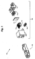
- Fig. 1 is an exploded perspective illustration of a communication connector 100 comprising a plug 102 and a jack 104, into which the plug 102 may be inserted.
- the plug 102 terminates a length of twisted pair communication cable (not shown), while the jack 104 may be connected to another piece of twisted pair communication cable or punch-down block (neither of which is shown in Fig. 1 )
- the jack 104 includes a main housing 106 and a bottom front sled 108 and top front sled 110 arranged to support eight plug interface contacts 112.
- the plug interface contacts 112 engage a PCB (Printed Circuit Board) 114 from the front via through-holes in the PCB 114.
- eight IDCs (Insulation Displacement Contacts) 116 engage the PCB 114 from the rear via additional through-holes in the PCB 114.
- a rear housing 118 having passageways for the IDCs 116 serves to provide an interface to a twisted pair communication cable or punch-down block.
- the general connector 100 Illustrated in Fig. 1 serves as background for the following discussion of improvements that may be made to the connector 100 to improve crosstalk performance.
- the simplified schematic diagram of Fig. 2 conceptually Illustrates parts of a connector assembly 300 that are primarily responsible for causing near end crosstalk, as well as those that may be used to compensate for near end crosstalk.
- the plug 302 and plug interface contacts 304 contribute respective capacitive and inductive crosstalk components C plug + L plug and C ontacts + L contacts , which may be approximated as a lumped crosstalk vector A (see Fig. 4 ).
- a compensation zone 306 on the PCB 308 provides crosstalk compensation to produce compensation vector B .
- a near end crosstalk zone 310 may contribute some additional crosstalk C to reduce the phase shift's effect on combined crosstalk.
- Fig. 3 illustrates vectors A , B , and C on a time axis. Note that the crosstalk vectors A and C are opposite in polarity from compensation vector B . The vectors' relative displacement along the time axis is caused by the physical distance of the compensation zone 306 and the crosstalk zone 310 from where the plug 302 meets the plug interface contacts 304 (causing propagation delays T 1 and T 2 ) and the relative permittivity of the intervening conduction paths.
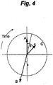
- Fig. 4 illustrates vectors A , B , and C on a polar axis, wherein displacement along the time axis of Fig. 3 has been translated to phase shift with reference to crosstalk vector A .
- the phase shift of B will grow toward A and that of C will grow in opposition to A .
- combined crosstalk can be minimized by designing the compensation zone and crosstalk zone so that
- Figs. 2-4 For frequencies up to about 300 MHz, the multi-zone crosstalk compensation technique illustrated in Figs. 2-4 is suitable to comply with Cat. 6 (TIA-568B) requirements for near end crosstalk. At higher frequencies, however, this technique is unsatisfactory.
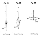
- Fig. 5 shows vectors A , B , and C on a polar axis, but with reference to compensation vector B .
- should be selected to be close to
- a and C experience larger phase shifts, evidenced by larger angles from vertical on the polar axis of Fig. 5 .
- Fig. 7 shows combined crosstalk performance of a typical Cat. 6 connector using the technique discussed with reference to Figs. 2-6 . Note the frequency at which the NEXT crosses the TIA-568B requirements limit.
- an additional coupling having a magnitude that grows disproportionate to frequency relative to a typical coupling may be included in the connector.
- one of the existing couplings can be modified to have a magnitude that varies disproportionally relative to the other couplings.
- Past typical connector couplings have been capacitive or mutually inductive, resulting In a magnitude that is proportional to frequency (approximately 20 dB per decade).
- the relative magnitudes of these typical connector couplings have remained approximately the same throughout various frequencies.
- FIGs. 8A-15 and their accompanying descriptions show alternative implementations of additional couplings having a magnitude that grows at a disproportionate rate relative to typical couplings, in response to frequency. Other implementations may also be used without departing from the spirit and scope of the present invention.
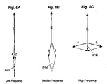
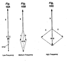
- Figs. 8A-10C are vector diagrams showing desired coupling characteristics. The description of Figs. 8A-10C is followed by a discussion of alternative methods for achieving the desired coupling characteristics.
- the additional coupling is a fourth coupling, D , having a magnitude with a frequency dependency that is different than that of A , B , and C .
- D a fourth coupling
- a , B , and C change at a rate of 20 dB per decade
- D could change at a lower rate, such as approximately 5 dB per decade.
- D could change at a higher rate (such as 30 dB per decade)
- a , B , and C remain relatively constant at 20 dB per decade.
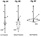
- compensation zone vector B is designed to have a magnitude with a frequency dependency that differs from that of A and C . For example, at low frequencies, if A and C change at a rate of 20 dB per decade, then B could be selected to vary at a lower rate, such as 15 dB per decade. At higher frequencies (such as those greater than a null frequency of interest), B could negatively change at a higher rate (such as -30 dB per decade), while A , and C remain relatively constant at 20 dB per decade. In contrast to the first implementation illustrated in Figs. 8A-8C , no additional coupling is needed in this second implementation.
- couplings A and C are selected to have a greater magnitude dependence on frequency than B at frequencies higher than the null frequency.
- a , B , and C could all change at a rate of 20 dB per decade.
- a and C could be selected to vary at a higher rate, such as 25 dB per decade, while B remains at approximately 20 dB per decade.
- the three Implementations described above are merely examples of possible implementations.
- the relative rates of change in magnitude given in dB per decade may vary from one application to the next, depending on the specific construction and materials of the connector assembly.
- the concept of relative magnitude variation over frequency may be applied to improve performance at frequencies other than at or around the null frequency.
- the null frequency was chosen for the above examples because it serves as a good starting point for making adjustments to improve high frequency operation. For current communications applications, null frequencies are generally observed around 100-250 MHz. Different connector designs will likely exhibit different null frequencies.
- the communication jack includes plug interface contacts for making electrical contact with the plug contacts in a plug, where the plug interface contacts and plug contacts introduce crosstalk to the connector.
- the crosstalk has an associated first frequency dependency based on a frequency of a communication signal being communicated.
- the jack has at least two crosstalk compensation zones, with at least one of the crosstalk compensation zones including a coupling having an associated second frequency dependency that substantially differs from the first frequency dependency associated with the plug Interface contacts and plug contacts.
- the first frequency dependency Is a magnitude change of approximately 20 dB per decade.
- the second frequency dependency is a magnitude that changes from approximately 0 dB per decade at a first frequency to approximately 20 dB per decade at a second frequency.
- the second frequency dependency is a magnitude that changes from approximately 20 dB per decade at a first frequency to less than 20 dB per decade at a second frequency.
- the second frequency dependency is a magnitude change of 20 dB per decade
- the first frequency dependency is a magnitude that changes from approximately 20 dB per decade at a first frequency to greater than 25 dB per decade at a second frequency.
- FIGs. 11A-11C illustrate an example of a first embodiment, in which a capacitance is placed in series with a mutual-inductive coupling.
- the mutual inductive coupling generates a current in the reverse direction of the current flowing through the capacitor, as shown in Fig. 11A , self inductance equivalent circuit 11 B, and impedance equivalent circuit 11 C.
- coupling through the capacitor is low; therefore, the reverse current generated in the secondary side of the inductance is also low.
- With rising frequency coupling through the capacitor will rise, increasing the current through the primary side of the inductor, thereby causing a higher reverse current through the secondary side of the inductor. As a result, coupling declines proportionally to frequency.
- Fig. 11A the "balanced source” 1262 shown in Fig. 11A is pairs 3 and 6, while the “balanced sink” 1264 is pairs 4 and 5.
- Fig. 12 shows an alternative arrangement of this embodiment, with pairs 3-4 and 5-6 illustrated on the left side.
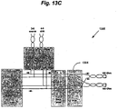
- Figs. 13A-13C illustrate how coupling alternative #1 may be implemented in either a back-rotated plug contact design 1300 or a front-rotated plug contact design 1302.
- Figs. 14A and 14B illustrate the location in a front-rotated design 1400 and a back-rotated design 1406 where the capacitive couplings may be located.
- the capacitance is placed in the tip nose region 1404 in a way that avoids physical interference with the plug 1402.
- the capacitance may again be located in the tip nose region 1410, which Is on the opposite side of the plug 1408 when compared to the front-rotated design.
- the capacitance may be placed above or below the contacts of the tip nose region 1410, so long as it does not physically interfere with insertion of the plug 1408.
- the placements shown in Figs. 14A and 14B result in capacitive couplings C35 and C46 (from pairs 3 and 5 and 4 and 6, respectively) and mutual inductive couplings M43 and M56 (from pairs 4 and 3 and 5 and 6, respectively).
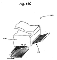
- Fig. 14C illustrates another location in an alternative front-rotated design 1412, as schematically illustrated In Fig. 12 , where the couplings may be located.
- the couplings are placed even closer to the point of electrical contact between the plug 1414 and the plug interface contacts 1416. This closer placement results from locating the couplings on the opposite side of the plug interface contacts 1416 from the plug 1414. This is achieved by moving the Inductive compensation from the conductors seen in the Tip Nose 1404 of Fig. 14A into a PCB, such as the flexible PCB shown in Fig. 24A . This results in reduced propagation delay and thus, reduced phase shift, which in turn provides better crosstalk performance.
- Coupling alternative #2 In a second alternative, the coupling takes the form of a capacitance that varies with frequency relative to other couplings.
- a capacitance is a capacitor having a dielectric with a permittivity that changes with frequency.
- Coupling alternative #3 According to a third alternative, the coupling is mutually inductive with a relative frequency-dependent inductance.
- an inductance is an inductive element composed of a ferrite material.
- Ferrites e.g. compounds with iron oxide and nickel-zinc or manganese-zinc
- a mixture of iron oxide and nickel-zinc has an initial permeability ranging from 10 to 1,500 over a range of 1 MHz to 1 GHz.
- Coupling alternative #4 In a fourth alternative, the coupling is a capacitance in series with one or more resistors that are frequency-dependent.
- a conductor or semiconductor resistor can be constructed to take advantage of the skin-effect to increase resistance at high frequencies.
- Coupling alternative #5 According to a fifth alternative, a capacitance is placed in series with a self-Inductive coupling. Increased inductance at higher frequencies will result In less coupling through the capacitance.
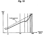
- Fig. 15 shows improved combined crosstalk performance of a typical Cat. 6 connector that may be obtained using the inventive techniques discussed above with reference to Figs. 8A-14 . Note that the frequency at which the NEXT crosses the TIA-568B requirements limit is much higher than in Fig. 7 .
- Figs. 16-28 illustrate physical changes that may be made to a jack to shorten the distance between the plug interface contacts and first compensation. These changes may be made in lieu of, or in combination with, the techniques described above. Optimal crosstalk performance will result from implementing the combination.
- Fig. 16 is a right-side schematic diagram illustrating a front rotated contact configuration 1600, including a plurality of plug interface contacts 1602 disposed in a contact carrier and front sled 1604 and a vertical interface PCB 1606 having a contact portion 1608 connected to a crosstalk compensation zone (not shown).
- the plug interface contacts 1602 are longer so that they come into contact with the contact portion 1608 of the vertical interface PCB 1606.
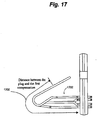
- the distance 1610 between the contact portion 1608 and the point at which contact is made between an inserted plug and the plug interface contacts 1602 is significantly smaller than for typical plug interface contacts, as can be seen by comparing the distance 1610 to distance 1700 in Fig. 17 .
- Fig. 17 includes inductive couplings shown generally at 1702, which assist in crosstalk compensation.
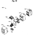
- Fig. 18 is an upper right-side exploded perspective view of a connector jack 1800 employing the above concept.
- the jack 1800 includes a bottom front sled 1804 and a top front sled 1808, each mechanically attached to a plurality of plug interface contacts 1806.
- a first end 1810 of the plug interface contacts 1806 may be inserted into through-holes in an interface PCB 1812, while a second end 1814 includes plug interface contact ends that are longer than for a typical jack to allow contact with a compensation zone on the interface PCB 1812.
- the sub-assembly comprising the bottom front sled 1804, plug interface contacts1806, top front sled 1808, and interface PCB 1812 is then inserted into a housing 1802.
- a rear sled 1820 is snapped into the housing 1802.
- a wire containment cap 1818 is configured to accept a four-pair twisted-pair communication cable for connection to the IDCs 1816 through the rear sled 1820. The wire containment cap 1818 may then be snapped onto the rear sled 1820, forming an integrated communication jack assembly.
- a second technique consists of placing the first compensation zone closer to the plug contact point by attaching a flexible PCB to the plug interface contacts.
- pad capacitors could be etched onto the flexible PCB to provide capacitive crosstalk compensation, thereby improving the electrical performance of the jack.
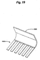
- Fig. 19 shows a six-position flexible PCB 1900 having six fingers 1902 that may be used to attach the flexible PCB 1900 to plug interface contacts 2000 carried in a front sled 2002, as shown in Fig. 20 . While a six-position flexible PCB 1900 is shown, an eight-position implementation is also possible. A six-position design may be preferred to avoid damage to standard RJ-45 jacks when a six-position RJ-45 plug is inserted. A standard six-position RJ-45 plug has plastic that protrudes further than the six contacts, which may lead to excessive displacement of plug interface contacts in the jack. The six-position flexible PCB 1900 allows plug interface contacts 1 and 8 to be displaced further than plug Interface contacts 2 though 7.
- the flexible PCB 1900 is preferably constructed of a layer of copper adhered to a polyester or polyamide substrate.
- the copper can be removed (e.g. by etching) in various configurations to create a crosstalk compensation zone.
- the fingers 1902 of the flexible PCB 1900 may be attached to the plug interface contacts 2000 in any of a number of ways. Attachment techniques may include ultrasonically welding or heat soldering, for example.
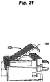
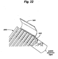
- Figs. 21 and 22 are perspective illustrations showing that the flexible PCB 1900 may be folded upward or downward. Other orientations and configurations are also possible.
- Fig. 22 also shows a suitable region of the plug interface contacts 2000 for attaching the fingers 1902 to the plug interface contacts 2000. Depending on the number of fingers 1902, the flexible PCB 1900 will be attached to the appropriate contacts for tuning.
- Figs. 23 and 24 are simplified right-side cross-sectional views illustrating that the flexible PCB 1900 may experience deflection upward ( Fig. 23 ) or downward ( Fig. 24 ) in the jack as the plug interface contacts travel in response to insertion of a plug.
- the flexible PCB 1900 follows the free deflection of each contact regardless of whether or not it is attached to the flexible PCB 1900.
- the fingers of the flexible PCB 1900 also accommodate the natural variation in contact deflection due to variation in the plug contact termination height. Clearance may need to be built Into the housing for the upward-deflecting flexible PCB 1900 of Fig. 23 or into the front top sled for the downward-deflecting flexible PCB 1900 of Fig. 24 .
- the vertically-spaced layout of plug interface contacts 2350 shown in Figs. 23 and 24 advantageously provides additional inductive crosstalk compensation. While this layout is preferred, other layouts may alternatively be used.
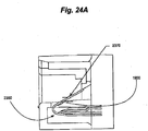
- Fig. 24A is a simplified right-side cross-sectional view illustrating an alternative placement of the flexible PCB 1900 on the plug interface contacts 2350.
- the flexible PCB 1900 and plug are on opposite sides of the plug Interface contacts 2350. This allows the couplings on the flexible PCB 1900 to be very close to the plug contact point 2370, resulting in reduced propagation delay and thus, reduced phase shift. This, in turn, provides better crosstalk performance.
- the flexible PCB 1900 may be designed to avoid contact with other parts of the jack, such as the lower part of the plug interface contacts 2350.
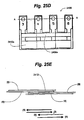
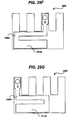
- Fig. 25A is an upper right-side perspective view
- Fig. 25B is a side view
- Fig. 25C is a front elevational view of one embodiment of a flexible PCB 2400 that may be utilized in accordance with the present invention to provide crosstalk compensation.
- the PCB 2400 includes a main portion 2402 and attachment fingers, such as the finger 2404.
- the main portion 2402 supports a plurality of capacitive plates (in this case, four plates, corresponding to plug interface contacts 3-6) to provide capacitive coupling.
- the leads to the capacitive plates provide an inductive coupling component as well.
- the fingers 2404 serve as an attachment mechanism for attaching the PCB 2400 to the plug interface contacts, using one of the schemes shown in Figs. 23-24A , for example. While any suitable attachment technique may be used, in the Illustrated embodiment, a resistance weld rivet 2406 is used. In addition to attaching the PCB 2400 to the plug interface contacts (or another conductor connected to the plug interface contacts), the rivet 2406 acts as a contact post for the capacitive plates and their leads. This is illustrated in Figs. 25B-I , which show four layers of capacitive plates 2412 and leads (2408a-d), through which the rivet 2406 protrudes to make appropriate contact in the fingers 2404.
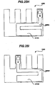
- Fig. 25D is a front elevational view of the PCB 2400 with the fingers in an unbent configuration, for ease of illustration.
- Fig. 25E is a cross-sectional view of the capacitive plates and leads as viewed upward from the bottom of the PCB 2400 toward line A/A in Fig. 25D .
- Fig. 25E does not show portions of the PCB 2400 that merely support the capacitive plates and leads or serve as a dielectric or insulator.
- Figs 25D-I show how the capacitive plates and leads are placed with respect to one another to result in a relatively high density of inductive coupling in a relatively short distance. For example, in Fig.
- the capacitive plate 2412a and lead 2408a for conductor 5 Is the topmost plate and lead shown, having a sideways "U" shape. The same "U" shape, but with varying orientation, is used for conductors 3, 4, and 6, as shown by the dashed and solid lines of Fig. 25D .
- the physical placement and overlapping area of the capacitive plates determines the amount of capacitive coupling.
- the separation of the leads from one another and the length of overlap determine the amount of inductive coupling.
- Fig. 25E also illustrates the relative direction of current flow in the respective leads, which provides a high density of inductive coupling.
- Figs. 25F-25I show, respectively, leads 2408a-d and capacitive plates 2412a-d associated with, respectively, fifth, third, sixth, and fourth conductors of an eight-conductor jack.
- Fig. 26 is an upper right-side exploded perspective view of a connector jack 2500 employing the flexible PCB concept.
- the jack 2500 includes a bottom front sled 2504 and a top front sled 2508, each mechanically attached to a plurality of plug interface contacts 2506.
- a first end 2510 of the plug Interface contacts 2506 may be inserted Into through-holes in an interface PCB 2512, while a second end 2514 is attached to a flexible PCB 2516 that provides crosstalk compensation.
- the sub-assembly comprising the bottom front sled 2504, plug interface contacts 2506, top front sled 2508, interface PCB 2512, and flexible PCB 2516 is then inserted into a housing 2502.
- a rear sled 2520 Is snapped into the housing 2502.
- a wire containment cap 2522 is configured to accept a four-pair twisted-pair communication cable (not shown) for connection to the IDCs 2518 through the rear sled 2520. The wire containment cap 2522 may then be snapped onto the rear sled 2520, forming an integrated communication jack assembly.
- FIGs. 19-26 are described with reference to a flexible PCB, this is merely one embodiment, and other embodiment using rigid PCBs or other compensation schemes may also be possible without departing from the intended scope of the invention.
- a flexible PCB may assist in meeting mechanical constraints that may exist in some connector designs.
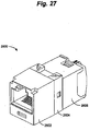
- Fig. 27 is an upper right-side perspective view of an assembled jack 2600.
- the jack 2600 includes a housing 2602 designed to accept a plug (not shown), a rear sled 2604, and a wire containment cap 2606 configured to accept a communication cable (not shown).
- the housing 2602, rear sled 2604, and wire containment cap 2606 latch together to form the assembled jack 2600.
- Fig. 28 is an upper right-side perspective exploded view of the jack 2600.
- the jack 2600 includes a PCB support 2708 designed to support a compensation PCB 2710 and an interface PCB 2712.
- a plurality of plug interface contacts 2714 have first ends 2716 pressed Into through-holes in the interface PCB 2712 and second ends 2718, at least some of which slide along the compensation PCB 2710 as a plug is received into the jack 2600.
- a plurality of IDCs 2720 are inserted in through-holes in the interface PCB 2712.
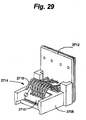
- FIG. 29 shows a closer perspective view of this plug interface contact sub-assembly (with the exception of IDCs 2720), which is inserted Into the housing 2602, prior to the rear sled 2604 being snapped onto the housing 2602.
- Assembly of the jack 2600 further includes positioning and installing a communication cable in the wire containment cap 2606, which is then snapped onto the rear sled 2604.
- the plug interface contact sub-assembly (without IDCs 2720) shown in Fig. 29 is designed to accommodate either 8-position plugs or 6-position plugs.
- a downward force causes contacts 2 through 7 to slide along the compensation PCB 2710.
- Contacts 1 and 8 deflect, but don't slide along the compensation PCB 2710.
- contacts 2 through 7 still slide along the compensation PCB 2710.
- contacts 1 and 8 deflect more than contacts 2 through 7, due to additional plastic material on the 6-position plug.
- the clearance over the compensation PCB 2710 provided by plug interface contacts 1 and 8 allows for this additional deflection, while maintaining adequate normal force between the plug and plug interface contacts 2714.
- the compensation circuits described above with reference to Figs. 11A-14C may be realized using standard layout and processing techniques composed of well-known electrical components. Additionally, generating mutual inductance circuits with substantial inductive properties to act as these compensators is relatively simple, when limits are not placed on the trace length of the circuit. However, the limited space provided by the PCB board attached to the plug interface contacts within the jack housing requires novel processing techniques and devices in order to create optimal inductive properties in as short of a trace as possible. These techniques should allow phase delay to be effectively introduced into the compensation circuitry despite the shortened trace lengths required of limited PCB area.
- One technique is to use magnetic ferrite materials to increase the mutual inductance between two signal traces.
- the magnetic material reacts strongly to the movement of electrical charges in a first signal trace, which also generate a magnetic flux. This magnetic flux is exhibited in the orientation of magnetic poles with the magnetic material, which then Influences the moving electrical charges associated with a second electrical trace.
- the magnetic material acts as a medium by which the two signal traces can be magneto-electrically coupled to a degree determined by the geometry and magnetic properties of the ferrous or magnetic material used.
- Fig. 30 shows an attachment of a ferrite material structure that serves as external inductor element for the two signal traces running through it.
- the core structure may be in the shape of several arches with the traces passing below the structure.
- the structure may have a solid half-cylindrical shape, or may be in the form of several rectangular arches.
- the external magnetic core may be composed of powdered iron, iron, nickel, steel, or a composite of these metals. Alternatively, it may be composed of another magnetic ferrite material with magneto-electric inductive properties.
- the magnetic core may be fabricated separately from the board, and may be soldered, glued, or snapped into place at prefabricated sites on the PCB. Attaching this component may be performed at a different site than that of the PCB manufacturer after PCB processing has been completed.
- Fig. 31 shows another method that can be used to increase mutual inductance between signal traces.
- no external components are required to generate the inductive coupling between the traces.
- the geometry of the traces themselves is altered to maximize coupling between the two signals.
- one trace is formed into a first winding, while the second trace is formed Into a second winding.
- the two windings overlap by a specified amount and geometry, allowing for an increased interaction between the two traces per trace length.
- different trace geometries may be used in order to increase the inductive coupling between the signals, such as elliptical or rectangular spirals.
- Fig. 32 illustrates two similar methods that may be used to increase the mutual inductance between signal traces. Like the first method presented, the methods shown in Fig. 32 utilize magnetic core materials to Increase the inductive coupling between two signal traces. In one method, the coupling is achieved by placing a magnetic coupler directly over two parallel traces.
- the magnetic material may be applied to the surface of the board using a variety of techniques. For example, the material may be melted and deposited onto the surface using a drop dispenser, it may be screened on, it may be added using an immersion and etch process, it may be rolled on, or the magnetic materials may be added using a similar process that allows for the patterned and localized deposition of material onto the surface of the circuit board.
- the magnetic coupling material may be inserted into the PCB through fabricated holes in the board.
- the holes may then be filled with magnetic material using, for example, a screening process.
- the magnetic material may be press fit into the PCB.
- the holes may be circular with cylindrical magnetic plugs used to fill the vacancies.
- the holes may consist of a different geometry that allows for inductive coupling between the traces through the magnetic core material.
- the magnetic material may be any magnetic ferrite material, such as those described above. Additionally, the magnetic components may ideally be incorporated into the PCB manufacturing process. However, the addition of the magnetic couplers may also take place after the board has been created at a different site from the PCB manufacturer.
- Fig. 33 illustrates a similar method to the embodiments shown in Figure 32 .
- the two signal traces are located in parallel on separate layers within the PCB. Holes are drilled into the PCB next to the signal traces and are then filled with magnetic material.
- the signal traces may be laid out so that they wrap around the magnetic cores, thereby increasing the amount of coupling induced by the magnetic material. Alternatively, other layouts may be used that either increase or decrease the amount of coupling, as required by the electrical specifications of the circuit.
- Filling the holes with magnetic core material may be accomplished via a screening process.
- the creation of the PCB holes and subsequent filling with magnetic material may be accomplished during the PCB manufacturing process, although such processing may also take place following the creation of the board and at a different site from the PCB manufacturer.
- Fig. 34 Another method for increasing the mutual inductance between signal traces is illustrated in Fig. 34 .
- the signal traces are fabricated onto PCB in the normal fashion.
- an internal layer of magnetic core material is laid on top of the board followed by another capping layer of PCB material.
- a layer of magnetic material may be embedded within the circuit board.
- the internal layer of magnetic core material may be patterned and selectively removed prior to the application of the capping PCB layer. This would allow the magnetic material to be present only in specific areas where increased inductive coupling is desired, and would also prevent inadvertent coupling between unrelated signal traces.
- the creation of this type of circuit would need to be performed at the PCB manufacturer site and may require additional processing steps to incorporate the magnetic material into the board.
- All of the above methods may be used to increase the inductive coupling per trace length in PCB manufactured circuits. These methods help to realize the crosstalk compensation circuits necessary for mitigating propagation delay effects at high frequencies in modular communication jacks.
- a communication jack comprising: plug interface contacts for making electrical contact with plug contacts in a plug, the plug interface contacts and plug contacts introducing crosstalk having an associated first frequency dependency based on a frequency of a communication signal being communicated; a plurality of crosstalk compensation zones, wherein at least one of the crosstalk compensation zones comprises a coupling having an associated second frequency dependency that substantially differs from the first frequency dependency.
- the plurality of crosstalk compensation zones includes a first zone to provide crosstalk compensation and a second zone to introduce additional crosstalk, and preferably the crosstalk introduced by the plug interface contacts and the plug contacts has an associated crosstalk vector, the first zone includes one or more couplings to provide a compensation vector, the additional crosstalk introduced by the second zone has an associated additional crosstalk vector, and the crosstalk vector is approximately equal in magnitude and opposite in polarity to the sum of the compensation vector and the additional crosstalk vector at a null frequency, and preferably the crosstalk vector is approximately equal in magnitude and opposite in polarity to the sum of the compensation vector and the additional crosstalk vector at a second frequency that is substantially greater than the first frequency.
- the first frequency dependency is a magnitude change of approximately 20 dB per decade
- the second frequency dependency is a magnitude that changes from approximately 0 dB per decade at a first frequency to approximately 20 dB per decade at a second frequency
- the plurality of crosstalk compensation zones includes a first zone to provide crosstalk compensation, a second zone to introduce additional crosstalk, and a third zone to compensate for a phase shift of the first zone at high frequencies
- the first and second zones have approximately the first frequency dependency and wherein the third zone has approximately the associated second frequency dependency that substantially differs from the first frequency dependency
- the crosstalk introduced by the plug interface contacts and the plug contacts has an associated crosstalk vector[A]
- the first zone includes one or more couplings to provide a compensation vector [B]
- the additional crosstalk introduced by the second zone has an associated additional crosstalk vector [C]
- the third zone includes one or more couplings to provide a phase shift compensation vector [D]
- the plurality of crosstalk compensation zones includes a first zone to provide crosstalk compensation and a second zone to introduce additional crosstalk, wherein the second zone has approximately the first frequency dependency, and wherein the first zone has approximately the associated second frequency dependency that substantially differs from the first frequency dependency, and preferably at a first frequency, the crosstalk introduced by the plug interface contacts and the plug contacts has an associated crosstalk vector [A], the first zone includes one or more couplings to provide a compensation vector [B], and the additional crosstalk introduced by the second zone has an associated additional crosstalk vector [C], and wherein, at a null frequency, [B] is selected to approximately equal [A] +[C], or wherein the first frequency dependency is a magnitude change of approximately 20 dB per decade, and wherein the second frequency dependency is a magnitude that changes from approximately 20 dB per decade at a first frequency to less than 20 dB per decade at a second frequency, or at a first frequency, the crosstalk introduced by the plug interface contacts and the plug contacts has an associated crosstalk vector
- At least one of the crosstalk compensation zones comprises a capacitance placed in series with a mutual-inductive coupling, and preferably the capacitance and mutual-inductive coupling are located at the opposite side of the plug-interface contacts from where the plug contacts electrically contact the plug interface contacts when the plug is inserted into the jack.
- At least one of the crosstalk compensation zones comprises a capacitance that varies with frequency relative to other capacitances in the jack, or the capacitance has a permittivity that changes with frequency, or at least one of the crosstalk compensation zones comprises an inductance that varies with frequency relative to other inductances in the jack, and preferably wherein the inductance includes a ferrite material.
- At least one of the crosstalk compensation zones comprises a capacitance in series with a frequency-dependent resistance, or at least one of the crosstalk compensation zones comprises a capacitance placed in series with a self-inductive coupling, or at least one of the crosstalk compensation zones is located less than approximately 0.508 cm (0.200 inches) from where the plug contacts electrically contact the plug interface contacts when the plug is inserted into the jack, or the communication jack further comprises first and second circuit boards, both in electrical contact with at least some of the plug interface contacts, and preferably the plug interface contacts end in through-holes located in the first circuit board, and wherein the second circuit board is a flexible printed circuit mechanically and electrically connected to the plug interface contacts less than approximately 0.200 inches from where the plug contacts electrically contact the plug interface contacts when the plug is inserted into the jack, or the plug interface contacts end in through-holes located in the first circuit board, and wherein the second circuit board is a flexible printed circuit mechanically and electrically connected at the opposite side of the plug-interface
- At least one of the circuit boards is attached to the plug interface contacts by flexible members, and preferably the flexible members attach to all but two of the plug interface contacts.
- an electrical connector comprising a plug having plug contacts, a jack having plug interface contacts, a first crosstalk compensation zone connected to at least two of the plug interface contacts, and a second crosstalk compensation zone connected to the at least two plug interface contacts, wherein the second crosstalk compensation zone comprises a purely resistive coupling between two signal traces in the second crosstalk compensation zone whereby impedance of the resistive coupling increases at high frequencies as a result of a skin-effect associated with the resistive coupling.
- a communication jack for communicating a signal comprising a first crosstalk compensation zone for offsetting crosstalk, a second crosstalk compensation zone to provide additional compensation to offset a phase-shift effect and a third crosstalk compensation zone to provide crosstalk compensation that adjusts with the frequency of the signal.
Landscapes
- Details Of Connecting Devices For Male And Female Coupling (AREA)
- Coupling Device And Connection With Printed Circuit (AREA)
Claims (14)
- Stecker-Buchse-Kombination umfassend eine Buchse (104) und einen Stecker (102, 302) mit Steckkontakten, wobei die Buchse umfasst: mehrere Steckerschnittstellenkontakte (304) in der Buchse, wobei die Steckerkontakte die Steckerschnittstellenkontakte an Stecker/Buchse-Schnittstellen der Steckerschnittstellenkontakte kontaktieren, wenn sie in die Buchse gesteckt werden; eine Kompensationszone (306) neben den Steckerschnittstellenkontakten; und eine Übersprechzone (310), die weiter von den Stecker/Buchse-Schnittstellen entfernt ist als die Kompensationszone, wobei die Kompensationszone eine erste Kompensationsanordnung enthält, die eine erste Kompensationskopplung mit einer ersten Größe bei irgendeiner bestimmten Frequenz der Normalbetriebsfrequenzen der Buchse und die Übersprechzone eine zweite Kompensationsanordnung enthält, die eine zweite Kompensationskupplung mit einer zweiten Größe bei derselben bestimmten Frequenz bereitstellt, dadurch gekennzeichnet, dass die Änderungsrate der ersten und/oder der zweiten Größe mit der Frequenz variiert.
- Stecker-Buchse-Kombination nach Anspruch 1, wobei die Änderungsrate der Größe der ersten oder zweiten Kompensationskupplung größer ist als die Änderungsrate der Größe der anderen ersten oder zweiten Kompensationskupplung bei einer der normalen Betriebsfrequenzen der Buchse (104).
- Stecker-Buchse-Kombination nach Anspruch 1, wobei die erste und/oder zweite Kompensationsstruktur eine Induktor-Kondensator-Kombination umfasst.
- Stecker-Buchse-Kombination nach Anspruch 1, wobei die erste und die zweite Kompensationskupplung entgegengesetzte Polarität zueinander aufweisen, und die Änderungsrate der zweiten Größe größer ist als die Änderungsrate der ersten Größe.
- Stecker-Buchse-Kombination nach Anspruch 1, wobei die Funktionen der ersten und zweiten Kompensationsstruktur unabhängig voneinander sind.
- Stecker-Buchse-Kombination nach Anspruch 1, wobei die Kompensationszone (306) eine Übersprechkompensationsschaltung enthält, die erste und zweite überlappende "U"-förmige Leiterbahnen umfasst, wobei jede "U"-förmige Leiterbahn einen ersten Schenkel, einen zweiten Schenkel, eine Basis, die den ersten und den zweiten Schenkel verbindet, und ein offenes Ende gegenüber der Basis definiert, die überlappenden Leiterbahnen so angeordnet sind, dass der erste Schenkel der ersten Leiterbahn direkt den ersten Schenkel der zweiten Leiterbahn überlappt, der zweite Schenkel der ersten Leiterbahn direkt den zweiten Schenkel der zweiten Leiterbahn überlappt und das offene Ende der ersten Leiterbahn direkt die Basis der zweiten Leiterbahn überlappt.
- Stecker-Buchse-Kombination nach Anspruch 6, wobei die Kompensationsschaltung auf einer flexiblen Leiterplatte (1900) angeordnet ist.
- Stecker-Buchse-Kombination nach Anspruch 7, wobei die flexible Leiterplatte (1900) an mindestens einem Buchsenkontakt der mehreren Buchsenkontakte an einer Stecker/Buchse-Schnittstelle angebracht ist.
- Stecker-Buchse-Kombination nach Anspruch 6, wobei die überlappenden Leiterbahnen so angeordnet sind, dass der im ersten Schenkel der ersten überlappenden Leiterbahn fließende Strom in die entgegengesetzte Richtung als der im ersten Schenkel der zweiten überlappenden Leiterbahn fließende Strom fließt.
- Stecker-Buchse-Kombination nach Anspruch 9, wobei die überlappenden Leiterbahnen so angeordnet sind, dass der im zweiten Schenkel der ersten überlappenden Leiterbahn fließende Strom in die entgegengesetzte Richtung als der im zweiten Schenkel der zweiten überlappenden Leiterbahn fließende Strom fließt.
- Stecker-Buchse-Kombination nach Anspruch 6, wobei der zweite Schenkel der ersten Leiterbahn dicker ist als der erste Schenkel der ersten Leiterbahn und der zweite Schenkel der zweiten Leiterbahn dicker ist als der erste Schenkel der zweiten Leiterbahn.
- Stecker-Buchse-Kombination nach Anspruch 6, die ferner dritte und vierte "U"-förmige Leiterbahnen umfasst, wobei jede "U"-förmige Leiterbahn einen ersten Schenkel, einen zweiten Schenkel, eine Basis, die den ersten und zweiten Schenkel verbindet, und ein offenes Ende gegenüber der Basis definiert, wobei die dritte und vierte Leiterbahn so angeordnet sind, dass der erste Schenkel der dritten Leiterbahn direkt den ersten Schenkel der vierten Leiterbahn überlappt, der zweite Schenkel der dritten Leiterbahn direkt den zweiten Schenkel der vierten Leiterbahn überlappt und das offene Ende der dritten Leiterbahn die Basis der vierten Leiterbahn überlappt.
- Stecker-Buchse-Kombination nach Anspruch 1, wobei die dritte und vierte Leiterbahn so angeordnet sind, dass der Strom im ersten Schenkel der dritten Leiterbahn in die entgegengesetzte Richtung als der Strom im ersten Schenkel der vierten Leiterbahn fließt.
- Stecker-Buchse-Kombination nach Anspruch 10, wobei die dritte und vierte Leiterbahn so angeordnet sind, dass der Strom im zweiten Schenkel der dritten Leiterbahn in die entgegengesetzte Richtung als der Strom im zweiten Schenkel der vierten Leiterbahn fließt.
Applications Claiming Priority (5)
| Application Number | Priority Date | Filing Date | Title |
|---|---|---|---|
| US55984604P | 2004-04-06 | 2004-04-06 | |
| US11/099,110 US7153168B2 (en) | 2004-04-06 | 2005-04-05 | Electrical connector with improved crosstalk compensation |
| EP05733102A EP1738442B1 (de) | 2004-04-06 | 2005-04-06 | Elektrischer verbinder mit verbesserter übersprechkompensation |
| EP08008642A EP1953879A1 (de) | 2004-04-06 | 2005-04-06 | Elektrischer Steckverbinder mit verbesserter Übersprechungskompensation |
| PCT/US2005/011728 WO2005101588A1 (en) | 2004-04-06 | 2005-04-06 | Electrical connector with improved crosstalk compensation |
Related Parent Applications (6)
| Application Number | Title | Priority Date | Filing Date |
|---|---|---|---|
| EP08008642A Division EP1953879A1 (de) | 2004-04-06 | 2005-04-06 | Elektrischer Steckverbinder mit verbesserter Übersprechungskompensation |
| EP05733102.7 Division | 2005-04-06 | ||
| EP05733102A Division EP1738442B1 (de) | 2004-04-06 | 2005-04-06 | Elektrischer verbinder mit verbesserter übersprechkompensation |
| EP80086424 Previously-Filed-Application | 2005-04-06 | ||
| EP80086424 Previously-Filed-Application | 2005-04-06 | ||
| EP08008642.4 Division | 2008-05-08 |
Publications (2)
| Publication Number | Publication Date |
|---|---|
| EP2282377A1 EP2282377A1 (de) | 2011-02-09 |
| EP2282377B1 true EP2282377B1 (de) | 2018-08-22 |
Family
ID=34965091
Family Applications (4)
| Application Number | Title | Priority Date | Filing Date |
|---|---|---|---|
| EP10184050A Ceased EP2270930A1 (de) | 2004-04-06 | 2005-04-06 | Elektrischer Steckverbinder mit verbesserter Übersprechungskompensation |
| EP10075635.2A Expired - Lifetime EP2282377B1 (de) | 2004-04-06 | 2005-04-06 | Elektrischer Steckverbinder mit verbesserter Übersprechungskompensation |
| EP08008642A Withdrawn EP1953879A1 (de) | 2004-04-06 | 2005-04-06 | Elektrischer Steckverbinder mit verbesserter Übersprechungskompensation |
| EP05733102A Expired - Lifetime EP1738442B1 (de) | 2004-04-06 | 2005-04-06 | Elektrischer verbinder mit verbesserter übersprechkompensation |
Family Applications Before (1)
| Application Number | Title | Priority Date | Filing Date |
|---|---|---|---|
| EP10184050A Ceased EP2270930A1 (de) | 2004-04-06 | 2005-04-06 | Elektrischer Steckverbinder mit verbesserter Übersprechungskompensation |
Family Applications After (2)
| Application Number | Title | Priority Date | Filing Date |
|---|---|---|---|
| EP08008642A Withdrawn EP1953879A1 (de) | 2004-04-06 | 2005-04-06 | Elektrischer Steckverbinder mit verbesserter Übersprechungskompensation |
| EP05733102A Expired - Lifetime EP1738442B1 (de) | 2004-04-06 | 2005-04-06 | Elektrischer verbinder mit verbesserter übersprechkompensation |
Country Status (6)
| Country | Link |
|---|---|
| US (7) | US7153168B2 (de) |
| EP (4) | EP2270930A1 (de) |
| JP (2) | JP4758422B2 (de) |
| AT (1) | ATE401683T1 (de) |
| DE (1) | DE602005008216D1 (de) |
| WO (1) | WO2005101588A1 (de) |
Families Citing this family (89)
| Publication number | Priority date | Publication date | Assignee | Title |
|---|---|---|---|---|
| US7265300B2 (en) * | 2003-03-21 | 2007-09-04 | Commscope Solutions Properties, Llc | Next high frequency improvement using hybrid substrates of two materials with different dielectric constant frequency slopes |
| US7182649B2 (en) | 2003-12-22 | 2007-02-27 | Panduit Corp. | Inductive and capacitive coupling balancing electrical connector |
| US7179131B2 (en) | 2004-02-12 | 2007-02-20 | Panduit Corp. | Methods and apparatus for reducing crosstalk in electrical connectors |
| US7153168B2 (en) * | 2004-04-06 | 2006-12-26 | Panduit Corp. | Electrical connector with improved crosstalk compensation |
| US7980900B2 (en) * | 2004-05-14 | 2011-07-19 | Commscope, Inc. Of North Carolina | Next high frequency improvement by using frequency dependent effective capacitance |
| US7190594B2 (en) * | 2004-05-14 | 2007-03-13 | Commscope Solutions Properties, Llc | Next high frequency improvement by using frequency dependent effective capacitance |
| EP1774625B1 (de) | 2004-07-13 | 2014-06-25 | Panduit Corporation | Nachrichtenverbindungsstecker mit flexibler leiterplatte |
| USD553572S1 (en) * | 2004-10-14 | 2007-10-23 | Cisco Technology, Inc. | Module assembly |
| US7175476B2 (en) * | 2005-01-11 | 2007-02-13 | Daeun Electronics Co., Ltd. | Crosstalk canceling pattern for high-speed communications and modular jack having the same |
| WO2006078760A1 (en) * | 2005-01-19 | 2006-07-27 | Panduit Corp. | Communication channels with suppression cores |
| US8094019B1 (en) * | 2005-11-29 | 2012-01-10 | Vanguard Products Group, Inc. | Self-shunting security device |
| US8011972B2 (en) * | 2006-02-13 | 2011-09-06 | Panduit Corp. | Connector with crosstalk compensation |
| US7367849B2 (en) * | 2006-03-07 | 2008-05-06 | Surtec Industries, Inc. | Electrical connector with shortened contact and crosstalk compensation |
| US20070197102A1 (en) * | 2006-02-23 | 2007-08-23 | Hung-Lin Wang | Connector for communications systems having category 6 performance using a single compensation signal or higher performance using plural compensation signals |
| US7381098B2 (en) * | 2006-04-11 | 2008-06-03 | Adc Telecommunications, Inc. | Telecommunications jack with crosstalk multi-zone crosstalk compensation and method for designing |
| US7479043B2 (en) * | 2006-05-08 | 2009-01-20 | The Siemon Company | Targeted compensation in telecommunications connectors |
| US7686650B2 (en) * | 2006-05-17 | 2010-03-30 | Bel Fuse Ltd. | High speed modular jack with flexible compensation circuit |
| JP4915585B2 (ja) * | 2006-09-21 | 2012-04-11 | パナソニック株式会社 | モジュラプラグ |
| WO2008048467A2 (en) | 2006-10-13 | 2008-04-24 | Adc Gmbh | Connecting hardware with multi-stage inductive and capacitive crosstalk compensation |
| DE102006056001B4 (de) * | 2006-11-24 | 2008-12-04 | Phoenix Contact Gmbh & Co. Kg | Konfektionierbarer Rundsteckverbinder für Ethernet |
| WO2008076813A2 (en) | 2006-12-13 | 2008-06-26 | Panduit Corp. | Communication jack having layered plug interface contacts |
| JP4449990B2 (ja) * | 2007-02-22 | 2010-04-14 | ソニー株式会社 | 接続構造及び信号伝送ケーブル |
| AU2012265604B2 (en) * | 2007-03-20 | 2013-05-30 | Panduit Corp. | Plug/jack system having PCB with lattice network |
| US7874878B2 (en) * | 2007-03-20 | 2011-01-25 | Panduit Corp. | Plug/jack system having PCB with lattice network |
| CN201039270Y (zh) * | 2007-04-03 | 2008-03-19 | 许庆仁 | 一种网络线接口 |
| US8758047B2 (en) | 2007-05-07 | 2014-06-24 | Ortronics, Inc. | Port replication assembly with adapter cable and related methods of use |
| US7628657B2 (en) * | 2007-05-07 | 2009-12-08 | Ortronics, Inc. | Connector assembly for use with plugs and preterminated cables |
| US8182294B2 (en) | 2007-05-07 | 2012-05-22 | Ortronics, Inc. | Connector assembly and related methods of use |
| US7481678B2 (en) * | 2007-06-14 | 2009-01-27 | Ortronics, Inc. | Modular insert and jack including bi-sectional lead frames |
| US7967645B2 (en) * | 2007-09-19 | 2011-06-28 | Leviton Manufacturing Co., Inc. | High speed data communications connector circuits, systems, and methods for reducing crosstalk in communications systems |
| CN101796694B (zh) * | 2007-09-19 | 2013-09-11 | 立维腾制造有限公司 | 在位于通信插座内的柔性印刷电路板上形成的内部串扰补偿电路和相关方法及系统 |
| US7736195B1 (en) | 2009-03-10 | 2010-06-15 | Leviton Manufacturing Co., Inc. | Circuits, systems and methods for implementing high speed data communications connectors that provide for reduced modal alien crosstalk in communications systems |
| CA2709965C (en) * | 2007-12-19 | 2016-07-19 | Panduit Corp. | Method and system for reducing common mode signal generation within a plug/jack connection |
| CN201178025Y (zh) * | 2008-01-05 | 2009-01-07 | 富士康(昆山)电脑接插件有限公司 | 磁性线圈模组及设有该模组的电连接器 |
| WO2009100296A1 (en) * | 2008-02-08 | 2009-08-13 | Panduit Corp. | Communications connector with improved contacts |
| AU2015200609B2 (en) * | 2008-02-12 | 2017-01-05 | Commscope Technologies Llc | Improved far end crosstalk compensation |
| US7841909B2 (en) * | 2008-02-12 | 2010-11-30 | Adc Gmbh | Multistage capacitive far end crosstalk compensation arrangement |
| US7641521B2 (en) * | 2008-04-15 | 2010-01-05 | Tyco Electronics Corporation | Electrical connector with compensation loops |
| US7976348B2 (en) * | 2008-05-07 | 2011-07-12 | Ortronics, Inc. | Modular insert and jack including moveable reactance section |
| US7601034B1 (en) | 2008-05-07 | 2009-10-13 | Ortronics, Inc. | Modular insert and jack including moveable reactance section |
| US7686649B2 (en) * | 2008-06-06 | 2010-03-30 | Tyco Electronics Corporation | Electrical connector with compensation component |
| KR101602719B1 (ko) * | 2008-08-13 | 2016-03-11 | 팬듀트 코포레이션 | 멀티스테이지 보상을 하는 통신 커넥터 |
| AU2009282836A1 (en) * | 2008-08-20 | 2010-02-25 | Panduit Corp. | High-speed connector with multi-stage compensation |
| US7794286B2 (en) * | 2008-12-12 | 2010-09-14 | Hubbell Incorporated | Electrical connector with separate contact mounting and compensation boards |
| KR20100081790A (ko) * | 2009-01-07 | 2010-07-15 | 삼성전기주식회사 | 휴대폰 케이스용 조성물 및 이를 이용한 휴대폰 케이스 제조 방법 |
| EP2209172A1 (de) | 2009-01-15 | 2010-07-21 | 3M Innovative Properties Company | Telekommunikationsbuchse mit einer Mehrschicht-Leiterplatte |
| US8047879B2 (en) * | 2009-01-26 | 2011-11-01 | Commscope, Inc. Of North Carolina | Printed wiring boards and communication connectors having series inductor-capacitor crosstalk compensation circuits that share a common inductor |
| IL200209A0 (en) * | 2009-08-03 | 2010-04-29 | Keshet Guy | Universal connector for installing domestic electric devices |
| GB0914025D0 (en) | 2009-08-11 | 2009-09-16 | 3M Innovative Properties Co | Telecommunications connector |
| US8128436B2 (en) * | 2009-08-25 | 2012-03-06 | Tyco Electronics Corporation | Electrical connectors with crosstalk compensation |
| US7967644B2 (en) | 2009-08-25 | 2011-06-28 | Tyco Electronics Corporation | Electrical connector with separable contacts |
| US8016621B2 (en) * | 2009-08-25 | 2011-09-13 | Tyco Electronics Corporation | Electrical connector having an electrically parallel compensation region |
| US8435082B2 (en) | 2010-08-03 | 2013-05-07 | Tyco Electronics Corporation | Electrical connectors and printed circuits having broadside-coupling regions |
| ES2608689T3 (es) | 2009-10-16 | 2017-04-12 | Adc Telecommunications, Inc. | Conectividad dirigida en sistemas eléctricos y sus métodos |
| MX2012004521A (es) | 2009-10-19 | 2012-07-23 | Adc Telecommunications Inc | Sistema de conectividad electrica gestionados. |
| US7850492B1 (en) | 2009-11-03 | 2010-12-14 | Panduit Corp. | Communication connector with improved crosstalk compensation |
| US7909657B1 (en) * | 2009-11-12 | 2011-03-22 | Hubbell Incorporated | Electrical connector with low-stress, reduced-electrical-length contacts |
| EP2403069B1 (de) * | 2010-07-02 | 2017-05-17 | Nexans | Kommunikationsanordnung mit einem Steckverbinder und einer Buchsenanordnung zur gemeinsamen Verbindung |
| US8696369B2 (en) | 2010-09-09 | 2014-04-15 | Adc Telecommunications, Inc. | Electrical plug with main contacts and retractable secondary contacts |
| WO2012054348A1 (en) | 2010-10-22 | 2012-04-26 | Adc Telecommunications, Inc. | Single-piece plug nose |
| WO2012078824A2 (en) | 2010-12-07 | 2012-06-14 | Carlyle, Inc. D/B/A Carlisle Interconnect Technologies | Electrical connector for high-speed data transmission |
| EP2487761B1 (de) | 2011-02-10 | 2013-07-31 | 3M Innovative Properties Company | Telekommunikationsverbinder |
| WO2012158806A2 (en) | 2011-05-17 | 2012-11-22 | Adc Telecommunications, Inc. | Component identification and tracking systems for telecommunication networks |
| MX2014006082A (es) | 2011-11-23 | 2014-06-23 | Panduit Corp | Red de compensacion que utiliza una red de compensacion ortogonal. |
| US9136647B2 (en) | 2012-06-01 | 2015-09-15 | Panduit Corp. | Communication connector with crosstalk compensation |
| US20140027155A1 (en) * | 2012-07-25 | 2014-01-30 | Ametek, Inc. | Differential mode signal connector and cable assembly |
| US8961239B2 (en) | 2012-09-07 | 2015-02-24 | Commscope, Inc. Of North Carolina | Communication jack having a plurality of contacts mounted on a flexible printed circuit board |
| US9306312B2 (en) | 2012-10-29 | 2016-04-05 | Carlisle Interconnect Technologies, Inc. | High density sealed electrical connector with multiple shielding strain relief devices |
| US9306333B2 (en) | 2012-10-29 | 2016-04-05 | Carlisle Interconnect Technologies, Inc. | High density sealed electrical connector with grounding contact for improved mechanical connection and shielding |
| US9246463B2 (en) | 2013-03-07 | 2016-01-26 | Panduit Corp. | Compensation networks and communication connectors using said compensation networks |
| US9379500B2 (en) | 2013-03-11 | 2016-06-28 | Panduit Corp. | Front sled assemblies for communication jacks and communication jacks having front sled assemblies |
| US8894447B2 (en) | 2013-03-14 | 2014-11-25 | Commscope, Inc. Of North Carolina | Communication plug having a plurality of coupled conductive paths |
| US8858267B2 (en) | 2013-03-14 | 2014-10-14 | Commscope, Inc. Of North Carolina | Communications plugs and patch cords with mode conversion control circuitry |
| US9257792B2 (en) | 2013-03-14 | 2016-02-09 | Panduit Corp. | Connectors and systems having improved crosstalk performance |
| US9246274B2 (en) * | 2013-03-15 | 2016-01-26 | Panduit Corp. | Communication connectors having crosstalk compensation networks |
| US8864532B2 (en) | 2013-03-15 | 2014-10-21 | Commscope, Inc. Of North Carolina | Communications jacks having low crosstalk and/or solder-less wire connection assemblies |
| US8979592B2 (en) | 2013-03-15 | 2015-03-17 | Carlisle Interconnect Technologies, Inc. | Electrical connector for high-speed data transmission |
| US9088106B2 (en) * | 2013-05-14 | 2015-07-21 | Commscope, Inc. Of North Carolina | Communications jacks having flexible printed circuit boards with common mode crosstalk compensation |
| CN106415944A (zh) | 2014-04-23 | 2017-02-15 | 泰科电子公司 | 具有屏蔽帽和屏蔽端子的电连接器 |
| WO2017015459A1 (en) | 2015-07-21 | 2017-01-26 | Bel Fuse (Macao Commercial Offshore) Limited | Modular connector plug for high speed data transmission networks |
| US9608379B1 (en) * | 2015-10-14 | 2017-03-28 | Leviton Manufacturing Co., Inc. | Communication connector |
| EP3375052A1 (de) | 2015-11-11 | 2018-09-19 | Bel Fuse (Macao Commercial Offshore) Limited | Modularer klinkensteckverbinder |
| US10637196B2 (en) | 2015-11-11 | 2020-04-28 | Bel Fuse (Macao Commercial Offshore) Limited | Modular jack contact assembly having controlled capacitive coupling positioned within a jack housing |
| US11817659B2 (en) | 2015-12-08 | 2023-11-14 | Panduit Corp. | RJ45 shuttered jacks and related communication systems |
| WO2018081712A1 (en) | 2016-10-31 | 2018-05-03 | Commscope Technologies Llc | Connector with capacitive crosstalk compensation |
| US10342142B2 (en) | 2017-07-28 | 2019-07-02 | International Business Machines Corporation | Implementing customized PCB via creation through use of magnetic pads |
| US10530106B2 (en) | 2018-01-31 | 2020-01-07 | Bel Fuse (Macao Commercial Offshore) Limited | Modular plug connector with multilayer PCB for very high speed applications |
| US11114796B2 (en) | 2018-12-04 | 2021-09-07 | Carlisle Interconnect Technologies, Inc. | Electrical connector with modular housing for accommodating various contact layouts |
| US11031738B1 (en) * | 2020-01-03 | 2021-06-08 | Jyh Eng Technology Co., Ltd. | Multiple socket panel device with anti-crosstalk shielding structure |
Family Cites Families (94)
| Publication number | Priority date | Publication date | Assignee | Title |
|---|---|---|---|---|
| GB238033A (en) * | 1924-06-04 | 1925-08-13 | Edward Bradford Maxted | Oxidation of alcohols and aldehydes |
| FR2646000B1 (fr) | 1989-04-14 | 1995-07-21 | Thomson Csf | Tete magnetique statique de lecture |
| US5006822A (en) * | 1990-01-03 | 1991-04-09 | Prabhakara Reddy | Hybrid RF coupling device with integrated capacitors and resistors |
| US5069641A (en) | 1990-02-03 | 1991-12-03 | Murata Manufacturing Co., Ltd. | Modular jack |
| US5163836A (en) | 1991-03-11 | 1992-11-17 | Apple Computer, Inc. | Integrated connector module with conductive elastomeric contacts |
| US5186647A (en) | 1992-02-24 | 1993-02-16 | At&T Bell Laboratories | High frequency electrical connector |
| US5299956B1 (en) | 1992-03-23 | 1995-10-24 | Superior Modular Prod Inc | Low cross talk electrical connector system |
| US5228872A (en) | 1992-05-05 | 1993-07-20 | Dan-Chief Enterprise Co., Ltd. | Shielded IDC type modular jack adapter |
| CA2072380C (en) | 1992-06-25 | 2000-08-01 | Michel Bohbot | Circuit assemblies of printed circuit boards and telecommunications connectors |
| US5432484A (en) * | 1992-08-20 | 1995-07-11 | Hubbell Incorporated | Connector for communication systems with cancelled crosstalk |
| GB2273397B (en) | 1992-11-16 | 1997-01-29 | Krone Ag | Electrical connectors |
| US5295869A (en) * | 1992-12-18 | 1994-03-22 | The Siemon Company | Electrically balanced connector assembly |
| US5269708A (en) | 1993-03-03 | 1993-12-14 | Adc Telecommunications, Inc. | Patch panel for high speed twisted pair |
| US6464529B1 (en) | 1993-03-12 | 2002-10-15 | Cekan/Cdt A/S | Connector element for high-speed data communications |
| US5362257A (en) * | 1993-07-08 | 1994-11-08 | The Whitaker Corporation | Communications connector terminal arrays having noise cancelling capabilities |
| US5470244A (en) | 1993-10-05 | 1995-11-28 | Thomas & Betts Corporation | Electrical connector having reduced cross-talk |
| US5503572A (en) | 1994-05-17 | 1996-04-02 | Mod-Tap Corporation | Communications connectors |
| DE9412794U1 (de) * | 1994-08-09 | 1995-09-07 | Krone Ag, 14167 Berlin | Leiterplatte für Steckverbinder |
| US5618185A (en) | 1995-03-15 | 1997-04-08 | Hubbell Incorporated | Crosstalk noise reduction connector for telecommunication system |
| GB9509886D0 (en) * | 1995-05-16 | 1995-07-12 | Amp Holland | Modular plug for high speed data transmission |
| US5586914A (en) | 1995-05-19 | 1996-12-24 | The Whitaker Corporation | Electrical connector and an associated method for compensating for crosstalk between a plurality of conductors |
| US5672074A (en) | 1995-06-22 | 1997-09-30 | Panduit Corp. | Connector mounting receptacles |
| US5791943A (en) | 1995-11-22 | 1998-08-11 | The Siemon Company | Reduced crosstalk modular outlet |
| US5769647A (en) | 1995-11-22 | 1998-06-23 | The Siemon Company | Modular outlet employing a door assembly |
| JP3802070B2 (ja) * | 1996-02-29 | 2006-07-26 | ザ ウィタカー コーポレーション | クロストーク減少のための非抵抗エネルギ結合 |
| US5716237A (en) | 1996-06-21 | 1998-02-10 | Lucent Technologies Inc. | Electrical connector with crosstalk compensation |
| US5779503A (en) | 1996-12-18 | 1998-07-14 | Nordx/Cdt, Inc. | High frequency connector with noise cancelling characteristics |
| US5797764A (en) | 1997-02-12 | 1998-08-25 | Homaco, Inc. | Low return loss and low crosstalk telecommunications electric circuit |
| DE19708798A1 (de) | 1997-03-05 | 1998-09-24 | Krone Ag | Anordnung von Kontaktpaaren zur Kompensation des Nahnebensprechens |
| US5997358A (en) * | 1997-09-02 | 1999-12-07 | Lucent Technologies Inc. | Electrical connector having time-delayed signal compensation |
| US5915989A (en) | 1997-05-19 | 1999-06-29 | Lucent Technologies Inc. | Connector with counter-balanced crosswalk compensation scheme |
| FR2768862B1 (fr) | 1997-09-22 | 1999-12-24 | Infra Sa | Prise de courant faible a capuchon arriere organisateur |
| US5971812A (en) * | 1997-11-25 | 1999-10-26 | The Whitaker Corporation | Modular plug having a circuit board |
| CA2311802A1 (en) | 1997-12-05 | 1999-06-17 | Lk A/S | A method of reducing high frequency coupling between pairs of conductors in a connector, and a connector for transferring differential signals |
| US5885111A (en) | 1998-01-13 | 1999-03-23 | Shiunn Yang Enterprise Co., Ltd. | Keystone jack for digital communication networks |
| US5930119A (en) | 1998-02-26 | 1999-07-27 | Arizona Digital, Inc. | Backplane having reduced LC product |
| AUPP224298A0 (en) | 1998-03-06 | 1998-04-02 | Power And Digital Instruments Pty. Ltd. | Improved manner of electrical connection |
| GB9807616D0 (en) | 1998-04-08 | 1998-06-10 | Weatherley Richard | Reduction of crosstalk in data transmission system |
| JP2003522368A (ja) | 1998-04-16 | 2003-07-22 | トーマス アンド ベッツ インターナショナル,インク. | 漏話低減電気ジャックおよびプラグコネクタ |
| DE19822630C1 (de) | 1998-05-20 | 2000-09-07 | Krone Gmbh | Anordnung von Kontaktpaaren zur Kompensation des Nahnebensprechens für eine elektrische Steckverbindung |
| US6057743A (en) | 1998-06-22 | 2000-05-02 | Hubbell Incorporation | Distributed noise reduction circuits in telecommunication system connector |
| US6371793B1 (en) | 1998-08-24 | 2002-04-16 | Panduit Corp. | Low crosstalk modular communication connector |
| US6356162B1 (en) | 1999-04-02 | 2002-03-12 | Nordx/Cdt, Inc. | Impedance compensation for a cable and connector |
| US6255593B1 (en) | 1998-09-29 | 2001-07-03 | Nordx/Cdt, Inc. | Method and apparatus for adjusting the coupling reactances between twisted pairs for achieving a desired level of crosstalk |
| IL142552A0 (en) | 1998-10-14 | 2002-03-10 | Stewart Connector Systems Inc | Modular electrical connector assemblies with magnetic filter and/or visual indicator |
| US6379175B1 (en) | 1998-10-29 | 2002-04-30 | Nordx/Cdt. Inc. | Fixture for controlling the trajectory of wires to reduce crosstalk |
| GB2343558B (en) | 1998-11-04 | 2002-10-30 | Itt Mfg Enterprises Inc | Electrical connector |
| US6409547B1 (en) | 1998-12-02 | 2002-06-25 | Nordx/Cdt, Inc. | Modular connectors with compensation structures |
| US6155881A (en) | 1999-02-02 | 2000-12-05 | Lucent Technologies Inc. | Electrical connector with signal compensation |
| US6483714B1 (en) * | 1999-02-24 | 2002-11-19 | Kyocera Corporation | Multilayered wiring board |
| FR2791185B1 (fr) | 1999-03-16 | 2001-06-01 | Infra Sa | Connecteur basse tension pourvu d'un adaptateur et adaptateur pour un tel connecteur |
| US6079996A (en) | 1999-04-15 | 2000-06-27 | Lucent Technologies Inc. | Selectable compatibility electrical connector jack |
| IL129883A0 (en) | 1999-05-10 | 2000-02-29 | Rit Techn Ltd | Cable organizer |
| US6168474B1 (en) | 1999-06-04 | 2001-01-02 | Lucent Technologies Inc. | Communications connector having crosstalk compensation |
| US6176742B1 (en) | 1999-06-25 | 2001-01-23 | Avaya Inc. | Capacitive crosstalk compensation arrangement for communication connectors |
| US6250968B1 (en) | 1999-07-14 | 2001-06-26 | Berg Technology, Inc. | Electrical connector system with cross-talk compensation |
| US6089923A (en) * | 1999-08-20 | 2000-07-18 | Adc Telecommunications, Inc. | Jack including crosstalk compensation for printed circuit board |
| US6196880B1 (en) | 1999-09-21 | 2001-03-06 | Avaya Technology Corp. | Communication connector assembly with crosstalk compensation |
| DE69925126T2 (de) | 1999-10-29 | 2005-09-22 | Nexans | Modularer Telekommunikationsverbinder mit Übersprechverringerung |
| WO2001052364A1 (en) | 2000-01-14 | 2001-07-19 | Panduit Corp. | Low crosstalk modular communication connector |
| JP4455711B2 (ja) | 2000-02-15 | 2010-04-21 | ヒロセ電機株式会社 | モジュラージャックコネクタ |
| US6533618B1 (en) | 2000-03-31 | 2003-03-18 | Ortronics, Inc. | Bi-directional balance low noise communication interface |
| WO2001080376A1 (en) | 2000-04-14 | 2001-10-25 | Tyco Electronics Corporation | Electrical connector for reducing crosstalk |
| US6402560B1 (en) | 2000-05-31 | 2002-06-11 | Avaya Technology Corp. | Communication connector with crosstalk compensation |
| AU2001267086A1 (en) | 2000-06-14 | 2001-12-24 | Rambus Inc. | Method and apparatus for transmitting data with reduced coupling noise |
| US6290524B1 (en) * | 2000-07-12 | 2001-09-18 | Molex Incorporated | System for varying capacitive coupling between electrical terminals |
| DE10051097C2 (de) | 2000-08-17 | 2002-11-28 | Krone Gmbh | Elektrischer Steckverbinder |
| US6379157B1 (en) | 2000-08-18 | 2002-04-30 | Leviton Manufacturing Co., Inc. | Communication connector with inductive compensation |
| US6350158B1 (en) | 2000-09-19 | 2002-02-26 | Avaya Technology Corp. | Low crosstalk communication connector |
| US6802743B2 (en) | 2000-09-29 | 2004-10-12 | Ortronics, Inc. | Low noise communication modular connector insert |
| EP1371115A2 (de) | 2001-03-12 | 2003-12-17 | Nordx/Cdt., Inc. | Jackverbinder mit elektrostatischem entladungsschutz |
| FR2823606A1 (fr) | 2001-04-17 | 2002-10-18 | Infra Sa | Connecteur femelle basse tension |
| US6464541B1 (en) | 2001-05-23 | 2002-10-15 | Avaya Technology Corp. | Simultaneous near-end and far-end crosstalk compensation in a communication connector |
| US6600865B2 (en) | 2001-06-21 | 2003-07-29 | Hon Hai Precision Ind. Co., Ltd. | Stacked GBIC guide rail assembly |
| IL145103A (en) | 2001-08-23 | 2010-05-17 | Rit Techn Ltd | High data rate interconnecting device |
| TW507971U (en) | 2001-09-13 | 2002-10-21 | Perfect Three Mfg Corp | Information connector with distribution terminal panel |
| GB2380334A (en) | 2001-09-28 | 2003-04-02 | Itt Mfg Enterprises Inc | Communication connector having crosstalk compensating means |
| US6881096B2 (en) | 2002-04-15 | 2005-04-19 | Lantronix, Inc. | Compact serial-to-ethernet conversion port |
| FR2841394B1 (fr) | 2002-06-24 | 2004-11-19 | Framatome Connectors Int | Dispositif de connexion pour circuit souple |
| US6641443B1 (en) | 2002-09-27 | 2003-11-04 | Leviton Manufacturing Co., Inc. | Electrical connector jack |
| US6736681B2 (en) | 2002-10-03 | 2004-05-18 | Avaya Technology Corp. | Communications connector that operates in multiple modes for handling multiple signal types |
| US6796847B2 (en) * | 2002-10-21 | 2004-09-28 | Hubbell Incorporated | Electrical connector for telecommunications applications |
| CN100429830C (zh) * | 2002-11-20 | 2008-10-29 | 西蒙公司 | 提供串扰补偿的电信连接器和印刷电路板 |
| US7265300B2 (en) | 2003-03-21 | 2007-09-04 | Commscope Solutions Properties, Llc | Next high frequency improvement using hybrid substrates of two materials with different dielectric constant frequency slopes |
| US6769937B1 (en) | 2003-05-13 | 2004-08-03 | Molex Incorporated | Modular jack assembly for jack plugs with varying numbers of wires |
| US7150657B2 (en) | 2003-05-23 | 2006-12-19 | Nordx/Cdt Inc. | Wire lead guide and method for terminating a communications cable |
| US20050101579A1 (en) | 2003-11-06 | 2005-05-12 | Shippen Eugene R. | Endometriosis treatment protocol |
| US7182649B2 (en) | 2003-12-22 | 2007-02-27 | Panduit Corp. | Inductive and capacitive coupling balancing electrical connector |
| US7179131B2 (en) | 2004-02-12 | 2007-02-20 | Panduit Corp. | Methods and apparatus for reducing crosstalk in electrical connectors |
| US7187766B2 (en) | 2004-02-20 | 2007-03-06 | Adc Incorporated | Methods and systems for compensating for alien crosstalk between connectors |
| WO2005091444A1 (en) | 2004-03-12 | 2005-09-29 | Panduit Corp. | Methods and apparatus for reducing crosstalk in electrical connectors |
| US7153168B2 (en) | 2004-04-06 | 2006-12-26 | Panduit Corp. | Electrical connector with improved crosstalk compensation |
| CA2464834A1 (en) | 2004-04-19 | 2005-10-19 | Nordx/Cdt Inc. | Connector |
| EP1774625B1 (de) | 2004-07-13 | 2014-06-25 | Panduit Corporation | Nachrichtenverbindungsstecker mit flexibler leiterplatte |
-
2005
- 2005-04-05 US US11/099,110 patent/US7153168B2/en not_active Expired - Lifetime
- 2005-04-06 EP EP10184050A patent/EP2270930A1/de not_active Ceased
- 2005-04-06 JP JP2007507489A patent/JP4758422B2/ja not_active Expired - Lifetime
- 2005-04-06 DE DE602005008216T patent/DE602005008216D1/de not_active Expired - Lifetime
- 2005-04-06 EP EP10075635.2A patent/EP2282377B1/de not_active Expired - Lifetime
- 2005-04-06 EP EP08008642A patent/EP1953879A1/de not_active Withdrawn
- 2005-04-06 AT AT05733102T patent/ATE401683T1/de not_active IP Right Cessation
- 2005-04-06 WO PCT/US2005/011728 patent/WO2005101588A1/en not_active Ceased
- 2005-04-06 EP EP05733102A patent/EP1738442B1/de not_active Expired - Lifetime
-
2006
- 2006-08-14 US US11/464,335 patent/US7309261B2/en not_active Expired - Fee Related
-
2007
- 2007-03-29 US US11/693,256 patent/US7384315B2/en not_active Expired - Lifetime
- 2007-10-29 US US11/926,987 patent/US7481681B2/en not_active Expired - Fee Related
- 2007-10-29 US US11/926,941 patent/US7442092B2/en not_active Expired - Fee Related
-
2008
- 2008-06-09 US US12/135,569 patent/US7520784B2/en not_active Expired - Fee Related
-
2009
- 2009-01-26 US US12/359,727 patent/US7591689B2/en not_active Expired - Fee Related
-
2010
- 2010-12-03 JP JP2010269873A patent/JP5133391B2/ja not_active Expired - Fee Related
Non-Patent Citations (1)
| Title |
|---|
| None * |
Also Published As
| Publication number | Publication date |
|---|---|
| JP2011082185A (ja) | 2011-04-21 |
| US7442092B2 (en) | 2008-10-28 |
| US7384315B2 (en) | 2008-06-10 |
| US7591689B2 (en) | 2009-09-22 |
| JP5133391B2 (ja) | 2013-01-30 |
| US7481681B2 (en) | 2009-01-27 |
| US20050277339A1 (en) | 2005-12-15 |
| JP4758422B2 (ja) | 2011-08-31 |
| US20080090467A1 (en) | 2008-04-17 |
| US7153168B2 (en) | 2006-12-26 |
| EP1953879A1 (de) | 2008-08-06 |
| US7309261B2 (en) | 2007-12-18 |
| US7520784B2 (en) | 2009-04-21 |
| US20060286873A1 (en) | 2006-12-21 |
| DE602005008216D1 (de) | 2008-08-28 |
| US20080242156A1 (en) | 2008-10-02 |
| US20090130914A1 (en) | 2009-05-21 |
| US20070173120A1 (en) | 2007-07-26 |
| JP2007533079A (ja) | 2007-11-15 |
| EP1738442B1 (de) | 2008-07-16 |
| WO2005101588A1 (en) | 2005-10-27 |
| EP1738442A1 (de) | 2007-01-03 |
| EP2282377A1 (de) | 2011-02-09 |
| US20080090466A1 (en) | 2008-04-17 |
| ATE401683T1 (de) | 2008-08-15 |
| EP2270930A1 (de) | 2011-01-05 |
Similar Documents
| Publication | Publication Date | Title |
|---|---|---|
| EP2282377B1 (de) | Elektrischer Steckverbinder mit verbesserter Übersprechungskompensation | |
| US7190594B2 (en) | Next high frequency improvement by using frequency dependent effective capacitance | |
| US8287317B2 (en) | High-speed connector with multi-stage compensation | |
| US9531128B2 (en) | Methods and apparatus for reducing crosstalk in electrical connectors | |
| US7154049B2 (en) | Apparatus for crosstalk compensation in a telecommunications connector | |
| US8272902B2 (en) | Communications connector with multi-stage compensation | |
| US7980900B2 (en) | Next high frequency improvement by using frequency dependent effective capacitance | |
| JP5460339B2 (ja) | 格子形回路網のpcbを有するプラグ/ジャックシステム | |
| JP2004507057A (ja) | モジュラーコネクタ | |
| JP2003522368A (ja) | 漏話低減電気ジャックおよびプラグコネクタ | |
| CN100530851C (zh) | 改进串扰补偿的电连接器 |
Legal Events
| Date | Code | Title | Description |
|---|---|---|---|
| PUAI | Public reference made under article 153(3) epc to a published international application that has entered the european phase |
Free format text: ORIGINAL CODE: 0009012 |
|
| AC | Divisional application: reference to earlier application |
Ref document number: 1953879 Country of ref document: EP Kind code of ref document: P Ref document number: 1738442 Country of ref document: EP Kind code of ref document: P |
|
| AK | Designated contracting states |
Kind code of ref document: A1 Designated state(s): AT BE BG CH CY CZ DE DK EE ES FI FR GB GR HU IE IS IT LI LT LU MC NL PL PT RO SE SI SK TR |
|
| 17P | Request for examination filed |
Effective date: 20110809 |
|
| 17Q | First examination report despatched |
Effective date: 20151027 |
|
| REG | Reference to a national code |
Ref country code: DE Ref legal event code: R079 Ref document number: 602005054483 Country of ref document: DE Free format text: PREVIOUS MAIN CLASS: H01R0013646000 Ipc: H01R0013719000 |
|
| GRAP | Despatch of communication of intention to grant a patent |
Free format text: ORIGINAL CODE: EPIDOSNIGR1 |
|
| STAA | Information on the status of an ep patent application or granted ep patent |
Free format text: STATUS: GRANT OF PATENT IS INTENDED |
|
| RIC1 | Information provided on ipc code assigned before grant |
Ipc: H01R 13/719 20110101AFI20180221BHEP Ipc: H01R 13/6466 20110101ALI20180221BHEP Ipc: H01R 24/64 20110101ALN20180221BHEP Ipc: H05K 1/02 20060101ALN20180221BHEP Ipc: H01R 13/6464 20110101ALI20180221BHEP |
|
| INTG | Intention to grant announced |
Effective date: 20180313 |
|
| GRAS | Grant fee paid |
Free format text: ORIGINAL CODE: EPIDOSNIGR3 |
|
| GRAA | (expected) grant |
Free format text: ORIGINAL CODE: 0009210 |
|
| STAA | Information on the status of an ep patent application or granted ep patent |
Free format text: STATUS: THE PATENT HAS BEEN GRANTED |
|
| AC | Divisional application: reference to earlier application |
Ref document number: 1738442 Country of ref document: EP Kind code of ref document: P Ref document number: 1953879 Country of ref document: EP Kind code of ref document: P |
|
| AK | Designated contracting states |
Kind code of ref document: B1 Designated state(s): AT BE BG CH CY CZ DE DK EE ES FI FR GB GR HU IE IS IT LI LT LU MC NL PL PT RO SE SI SK TR |
|
| REG | Reference to a national code |
Ref country code: GB Ref legal event code: FG4D |
|
| REG | Reference to a national code |
Ref country code: CH Ref legal event code: EP |
|
| REG | Reference to a national code |
Ref country code: DE Ref legal event code: R096 Ref document number: 602005054483 Country of ref document: DE |
|
| REG | Reference to a national code |
Ref country code: AT Ref legal event code: REF Ref document number: 1033554 Country of ref document: AT Kind code of ref document: T Effective date: 20180915 |
|
| REG | Reference to a national code |
Ref country code: IE Ref legal event code: FG4D |
|
| REG | Reference to a national code |
Ref country code: NL Ref legal event code: MP Effective date: 20180822 |
|
| REG | Reference to a national code |
Ref country code: LT Ref legal event code: MG4D |
|
| PG25 | Lapsed in a contracting state [announced via postgrant information from national office to epo] |
Ref country code: IS Free format text: LAPSE BECAUSE OF FAILURE TO SUBMIT A TRANSLATION OF THE DESCRIPTION OR TO PAY THE FEE WITHIN THE PRESCRIBED TIME-LIMIT Effective date: 20181222 Ref country code: FI Free format text: LAPSE BECAUSE OF FAILURE TO SUBMIT A TRANSLATION OF THE DESCRIPTION OR TO PAY THE FEE WITHIN THE PRESCRIBED TIME-LIMIT Effective date: 20180822 Ref country code: GR Free format text: LAPSE BECAUSE OF FAILURE TO SUBMIT A TRANSLATION OF THE DESCRIPTION OR TO PAY THE FEE WITHIN THE PRESCRIBED TIME-LIMIT Effective date: 20181123 Ref country code: BG Free format text: LAPSE BECAUSE OF FAILURE TO SUBMIT A TRANSLATION OF THE DESCRIPTION OR TO PAY THE FEE WITHIN THE PRESCRIBED TIME-LIMIT Effective date: 20181122 Ref country code: SE Free format text: LAPSE BECAUSE OF FAILURE TO SUBMIT A TRANSLATION OF THE DESCRIPTION OR TO PAY THE FEE WITHIN THE PRESCRIBED TIME-LIMIT Effective date: 20180822 Ref country code: LT Free format text: LAPSE BECAUSE OF FAILURE TO SUBMIT A TRANSLATION OF THE DESCRIPTION OR TO PAY THE FEE WITHIN THE PRESCRIBED TIME-LIMIT Effective date: 20180822 Ref country code: NL Free format text: LAPSE BECAUSE OF FAILURE TO SUBMIT A TRANSLATION OF THE DESCRIPTION OR TO PAY THE FEE WITHIN THE PRESCRIBED TIME-LIMIT Effective date: 20180822 |
|
| REG | Reference to a national code |
Ref country code: AT Ref legal event code: MK05 Ref document number: 1033554 Country of ref document: AT Kind code of ref document: T Effective date: 20180822 |
|
| PG25 | Lapsed in a contracting state [announced via postgrant information from national office to epo] |
Ref country code: ES Free format text: LAPSE BECAUSE OF FAILURE TO SUBMIT A TRANSLATION OF THE DESCRIPTION OR TO PAY THE FEE WITHIN THE PRESCRIBED TIME-LIMIT Effective date: 20180822 |
|
| PG25 | Lapsed in a contracting state [announced via postgrant information from national office to epo] |
Ref country code: RO Free format text: LAPSE BECAUSE OF FAILURE TO SUBMIT A TRANSLATION OF THE DESCRIPTION OR TO PAY THE FEE WITHIN THE PRESCRIBED TIME-LIMIT Effective date: 20180822 Ref country code: CZ Free format text: LAPSE BECAUSE OF FAILURE TO SUBMIT A TRANSLATION OF THE DESCRIPTION OR TO PAY THE FEE WITHIN THE PRESCRIBED TIME-LIMIT Effective date: 20180822 Ref country code: PL Free format text: LAPSE BECAUSE OF FAILURE TO SUBMIT A TRANSLATION OF THE DESCRIPTION OR TO PAY THE FEE WITHIN THE PRESCRIBED TIME-LIMIT Effective date: 20180822 Ref country code: EE Free format text: LAPSE BECAUSE OF FAILURE TO SUBMIT A TRANSLATION OF THE DESCRIPTION OR TO PAY THE FEE WITHIN THE PRESCRIBED TIME-LIMIT Effective date: 20180822 Ref country code: AT Free format text: LAPSE BECAUSE OF FAILURE TO SUBMIT A TRANSLATION OF THE DESCRIPTION OR TO PAY THE FEE WITHIN THE PRESCRIBED TIME-LIMIT Effective date: 20180822 Ref country code: IT Free format text: LAPSE BECAUSE OF FAILURE TO SUBMIT A TRANSLATION OF THE DESCRIPTION OR TO PAY THE FEE WITHIN THE PRESCRIBED TIME-LIMIT Effective date: 20180822 |
|
| REG | Reference to a national code |
Ref country code: DE Ref legal event code: R097 Ref document number: 602005054483 Country of ref document: DE |
|
| PG25 | Lapsed in a contracting state [announced via postgrant information from national office to epo] |
Ref country code: DK Free format text: LAPSE BECAUSE OF FAILURE TO SUBMIT A TRANSLATION OF THE DESCRIPTION OR TO PAY THE FEE WITHIN THE PRESCRIBED TIME-LIMIT Effective date: 20180822 Ref country code: SK Free format text: LAPSE BECAUSE OF FAILURE TO SUBMIT A TRANSLATION OF THE DESCRIPTION OR TO PAY THE FEE WITHIN THE PRESCRIBED TIME-LIMIT Effective date: 20180822 |
|
| PLBE | No opposition filed within time limit |
Free format text: ORIGINAL CODE: 0009261 |
|
| STAA | Information on the status of an ep patent application or granted ep patent |
Free format text: STATUS: NO OPPOSITION FILED WITHIN TIME LIMIT |
|
| 26N | No opposition filed |
Effective date: 20190523 |
|
| PGFP | Annual fee paid to national office [announced via postgrant information from national office to epo] |
Ref country code: DE Payment date: 20190429 Year of fee payment: 15 |
|
| PG25 | Lapsed in a contracting state [announced via postgrant information from national office to epo] |
Ref country code: SI Free format text: LAPSE BECAUSE OF FAILURE TO SUBMIT A TRANSLATION OF THE DESCRIPTION OR TO PAY THE FEE WITHIN THE PRESCRIBED TIME-LIMIT Effective date: 20180822 |
|
| PGFP | Annual fee paid to national office [announced via postgrant information from national office to epo] |
Ref country code: FR Payment date: 20190425 Year of fee payment: 15 |
|
| PGFP | Annual fee paid to national office [announced via postgrant information from national office to epo] |
Ref country code: GB Payment date: 20190429 Year of fee payment: 15 |
|
| REG | Reference to a national code |
Ref country code: CH Ref legal event code: PL |
|
| REG | Reference to a national code |
Ref country code: BE Ref legal event code: MM Effective date: 20190430 |
|
| PG25 | Lapsed in a contracting state [announced via postgrant information from national office to epo] |
Ref country code: LU Free format text: LAPSE BECAUSE OF NON-PAYMENT OF DUE FEES Effective date: 20190406 Ref country code: MC Free format text: LAPSE BECAUSE OF FAILURE TO SUBMIT A TRANSLATION OF THE DESCRIPTION OR TO PAY THE FEE WITHIN THE PRESCRIBED TIME-LIMIT Effective date: 20180822 |
|
| PG25 | Lapsed in a contracting state [announced via postgrant information from national office to epo] |
Ref country code: LI Free format text: LAPSE BECAUSE OF NON-PAYMENT OF DUE FEES Effective date: 20190430 Ref country code: CH Free format text: LAPSE BECAUSE OF NON-PAYMENT OF DUE FEES Effective date: 20190430 |
|
| PG25 | Lapsed in a contracting state [announced via postgrant information from national office to epo] |
Ref country code: BE Free format text: LAPSE BECAUSE OF NON-PAYMENT OF DUE FEES Effective date: 20190430 |
|
| PG25 | Lapsed in a contracting state [announced via postgrant information from national office to epo] |
Ref country code: TR Free format text: LAPSE BECAUSE OF FAILURE TO SUBMIT A TRANSLATION OF THE DESCRIPTION OR TO PAY THE FEE WITHIN THE PRESCRIBED TIME-LIMIT Effective date: 20180822 |
|
| PG25 | Lapsed in a contracting state [announced via postgrant information from national office to epo] |
Ref country code: IE Free format text: LAPSE BECAUSE OF NON-PAYMENT OF DUE FEES Effective date: 20190406 |
|
| PG25 | Lapsed in a contracting state [announced via postgrant information from national office to epo] |
Ref country code: PT Free format text: LAPSE BECAUSE OF FAILURE TO SUBMIT A TRANSLATION OF THE DESCRIPTION OR TO PAY THE FEE WITHIN THE PRESCRIBED TIME-LIMIT Effective date: 20181222 |
|
| REG | Reference to a national code |
Ref country code: DE Ref legal event code: R119 Ref document number: 602005054483 Country of ref document: DE |
|
| PG25 | Lapsed in a contracting state [announced via postgrant information from national office to epo] |
Ref country code: DE Free format text: LAPSE BECAUSE OF NON-PAYMENT OF DUE FEES Effective date: 20201103 Ref country code: FR Free format text: LAPSE BECAUSE OF NON-PAYMENT OF DUE FEES Effective date: 20200430 |
|
| GBPC | Gb: european patent ceased through non-payment of renewal fee |
Effective date: 20200406 |
|
| PG25 | Lapsed in a contracting state [announced via postgrant information from national office to epo] |
Ref country code: GB Free format text: LAPSE BECAUSE OF NON-PAYMENT OF DUE FEES Effective date: 20200406 |
|
| PG25 | Lapsed in a contracting state [announced via postgrant information from national office to epo] |
Ref country code: CY Free format text: LAPSE BECAUSE OF FAILURE TO SUBMIT A TRANSLATION OF THE DESCRIPTION OR TO PAY THE FEE WITHIN THE PRESCRIBED TIME-LIMIT Effective date: 20180822 |
|
| PG25 | Lapsed in a contracting state [announced via postgrant information from national office to epo] |
Ref country code: HU Free format text: LAPSE BECAUSE OF FAILURE TO SUBMIT A TRANSLATION OF THE DESCRIPTION OR TO PAY THE FEE WITHIN THE PRESCRIBED TIME-LIMIT; INVALID AB INITIO Effective date: 20050406 |