EP2283395B1 - Polymer-stift-lithographie - Google Patents
Polymer-stift-lithographie Download PDFInfo
- Publication number
- EP2283395B1 EP2283395B1 EP09735282.7A EP09735282A EP2283395B1 EP 2283395 B1 EP2283395 B1 EP 2283395B1 EP 09735282 A EP09735282 A EP 09735282A EP 2283395 B1 EP2283395 B1 EP 2283395B1
- Authority
- EP
- European Patent Office
- Prior art keywords
- tips
- tip array
- substrate surface
- array
- tip
- Prior art date
- Legal status (The legal status is an assumption and is not a legal conclusion. Google has not performed a legal analysis and makes no representation as to the accuracy of the status listed.)
- Active
Links
Images



Classifications
-
- G—PHYSICS
- G03—PHOTOGRAPHY; CINEMATOGRAPHY; ANALOGOUS TECHNIQUES USING WAVES OTHER THAN OPTICAL WAVES; ELECTROGRAPHY; HOLOGRAPHY
- G03F—PHOTOMECHANICAL PRODUCTION OF TEXTURED OR PATTERNED SURFACES, e.g. FOR PRINTING, FOR PROCESSING OF SEMICONDUCTOR DEVICES; MATERIALS THEREFOR; ORIGINALS THEREFOR; APPARATUS SPECIALLY ADAPTED THEREFOR
- G03F7/00—Photomechanical, e.g. photolithographic, production of textured or patterned surfaces, e.g. printing surfaces; Materials therefor, e.g. comprising photoresists; Apparatus specially adapted therefor
- G03F7/0002—Lithographic processes using patterning methods other than those involving the exposure to radiation, e.g. by stamping
-
- B—PERFORMING OPERATIONS; TRANSPORTING
- B29—WORKING OF PLASTICS; WORKING OF SUBSTANCES IN A PLASTIC STATE IN GENERAL
- B29C—SHAPING OR JOINING OF PLASTICS; SHAPING OF MATERIAL IN A PLASTIC STATE, NOT OTHERWISE PROVIDED FOR; AFTER-TREATMENT OF THE SHAPED PRODUCTS, e.g. REPAIRING
- B29C59/00—Surface shaping of articles, e.g. embossing; Apparatus therefor
- B29C59/02—Surface shaping of articles, e.g. embossing; Apparatus therefor by mechanical means, e.g. pressing
-
- B—PERFORMING OPERATIONS; TRANSPORTING
- B29—WORKING OF PLASTICS; WORKING OF SUBSTANCES IN A PLASTIC STATE IN GENERAL
- B29C—SHAPING OR JOINING OF PLASTICS; SHAPING OF MATERIAL IN A PLASTIC STATE, NOT OTHERWISE PROVIDED FOR; AFTER-TREATMENT OF THE SHAPED PRODUCTS, e.g. REPAIRING
- B29C33/00—Moulds or cores; Details thereof or accessories therefor
- B29C33/38—Moulds or cores; Details thereof or accessories therefor characterised by the material or the manufacturing process
-
- B—PERFORMING OPERATIONS; TRANSPORTING
- B82—NANOTECHNOLOGY
- B82Y—SPECIFIC USES OR APPLICATIONS OF NANOSTRUCTURES; MEASUREMENT OR ANALYSIS OF NANOSTRUCTURES; MANUFACTURE OR TREATMENT OF NANOSTRUCTURES
- B82Y10/00—Nanotechnology for information processing, storage or transmission, e.g. quantum computing or single electron logic
-
- B—PERFORMING OPERATIONS; TRANSPORTING
- B82—NANOTECHNOLOGY
- B82Y—SPECIFIC USES OR APPLICATIONS OF NANOSTRUCTURES; MEASUREMENT OR ANALYSIS OF NANOSTRUCTURES; MANUFACTURE OR TREATMENT OF NANOSTRUCTURES
- B82Y40/00—Manufacture or treatment of nanostructures
-
- B—PERFORMING OPERATIONS; TRANSPORTING
- B82—NANOTECHNOLOGY
- B82Y—SPECIFIC USES OR APPLICATIONS OF NANOSTRUCTURES; MEASUREMENT OR ANALYSIS OF NANOSTRUCTURES; MANUFACTURE OR TREATMENT OF NANOSTRUCTURES
- B82Y30/00—Nanotechnology for materials or surface science, e.g. nanocomposites
-
- Y—GENERAL TAGGING OF NEW TECHNOLOGICAL DEVELOPMENTS; GENERAL TAGGING OF CROSS-SECTIONAL TECHNOLOGIES SPANNING OVER SEVERAL SECTIONS OF THE IPC; TECHNICAL SUBJECTS COVERED BY FORMER USPC CROSS-REFERENCE ART COLLECTIONS [XRACs] AND DIGESTS
- Y10—TECHNICAL SUBJECTS COVERED BY FORMER USPC
- Y10S—TECHNICAL SUBJECTS COVERED BY FORMER USPC CROSS-REFERENCE ART COLLECTIONS [XRACs] AND DIGESTS
- Y10S977/00—Nanotechnology
- Y10S977/84—Manufacture, treatment, or detection of nanostructure
- Y10S977/849—Manufacture, treatment, or detection of nanostructure with scanning probe
- Y10S977/855—Manufacture, treatment, or detection of nanostructure with scanning probe for manufacture of nanostructure
- Y10S977/856—Manufacture, treatment, or detection of nanostructure with scanning probe for manufacture of nanostructure including etching/cutting
-
- Y—GENERAL TAGGING OF NEW TECHNOLOGICAL DEVELOPMENTS; GENERAL TAGGING OF CROSS-SECTIONAL TECHNOLOGIES SPANNING OVER SEVERAL SECTIONS OF THE IPC; TECHNICAL SUBJECTS COVERED BY FORMER USPC CROSS-REFERENCE ART COLLECTIONS [XRACs] AND DIGESTS
- Y10—TECHNICAL SUBJECTS COVERED BY FORMER USPC
- Y10S—TECHNICAL SUBJECTS COVERED BY FORMER USPC CROSS-REFERENCE ART COLLECTIONS [XRACs] AND DIGESTS
- Y10S977/00—Nanotechnology
- Y10S977/84—Manufacture, treatment, or detection of nanostructure
- Y10S977/849—Manufacture, treatment, or detection of nanostructure with scanning probe
- Y10S977/86—Scanning probe structure
- Y10S977/874—Probe tip array
-
- Y—GENERAL TAGGING OF NEW TECHNOLOGICAL DEVELOPMENTS; GENERAL TAGGING OF CROSS-SECTIONAL TECHNOLOGIES SPANNING OVER SEVERAL SECTIONS OF THE IPC; TECHNICAL SUBJECTS COVERED BY FORMER USPC CROSS-REFERENCE ART COLLECTIONS [XRACs] AND DIGESTS
- Y10—TECHNICAL SUBJECTS COVERED BY FORMER USPC
- Y10S—TECHNICAL SUBJECTS COVERED BY FORMER USPC CROSS-REFERENCE ART COLLECTIONS [XRACs] AND DIGESTS
- Y10S977/00—Nanotechnology
- Y10S977/84—Manufacture, treatment, or detection of nanostructure
- Y10S977/849—Manufacture, treatment, or detection of nanostructure with scanning probe
- Y10S977/86—Scanning probe structure
- Y10S977/875—Scanning probe structure with tip detail
- Y10S977/878—Shape/taper
-
- Y—GENERAL TAGGING OF NEW TECHNOLOGICAL DEVELOPMENTS; GENERAL TAGGING OF CROSS-SECTIONAL TECHNOLOGIES SPANNING OVER SEVERAL SECTIONS OF THE IPC; TECHNICAL SUBJECTS COVERED BY FORMER USPC CROSS-REFERENCE ART COLLECTIONS [XRACs] AND DIGESTS
- Y10—TECHNICAL SUBJECTS COVERED BY FORMER USPC
- Y10S—TECHNICAL SUBJECTS COVERED BY FORMER USPC CROSS-REFERENCE ART COLLECTIONS [XRACs] AND DIGESTS
- Y10S977/00—Nanotechnology
- Y10S977/84—Manufacture, treatment, or detection of nanostructure
- Y10S977/887—Nanoimprint lithography, i.e. nanostamp
-
- Y—GENERAL TAGGING OF NEW TECHNOLOGICAL DEVELOPMENTS; GENERAL TAGGING OF CROSS-SECTIONAL TECHNOLOGIES SPANNING OVER SEVERAL SECTIONS OF THE IPC; TECHNICAL SUBJECTS COVERED BY FORMER USPC CROSS-REFERENCE ART COLLECTIONS [XRACs] AND DIGESTS
- Y10—TECHNICAL SUBJECTS COVERED BY FORMER USPC
- Y10S—TECHNICAL SUBJECTS COVERED BY FORMER USPC CROSS-REFERENCE ART COLLECTIONS [XRACs] AND DIGESTS
- Y10S977/00—Nanotechnology
- Y10S977/84—Manufacture, treatment, or detection of nanostructure
- Y10S977/888—Shaping or removal of materials, e.g. etching
-
- Y—GENERAL TAGGING OF NEW TECHNOLOGICAL DEVELOPMENTS; GENERAL TAGGING OF CROSS-SECTIONAL TECHNOLOGIES SPANNING OVER SEVERAL SECTIONS OF THE IPC; TECHNICAL SUBJECTS COVERED BY FORMER USPC CROSS-REFERENCE ART COLLECTIONS [XRACs] AND DIGESTS
- Y10—TECHNICAL SUBJECTS COVERED BY FORMER USPC
- Y10S—TECHNICAL SUBJECTS COVERED BY FORMER USPC CROSS-REFERENCE ART COLLECTIONS [XRACs] AND DIGESTS
- Y10S977/00—Nanotechnology
- Y10S977/902—Specified use of nanostructure
Definitions
- Lithography is used in many areas of modern science and technology, including the production of integrated circuits, information storage devices, video screens, micro-electromechanical systems (MEMS), miniaturized sensors, microfluidic devices, biochips, photonic bandgap structures, and diffractive optical elements (1-6).
- lithography can be divided into two categories based on patterning strategy: parallel replication and serial writing.
- Parallel replication methods such as photolithography (7), contact printing (8-11), and nanoimprint lithography (12) are useful for high throughput, large area patterning.
- most of these methods can only duplicate patterns, which are predefined by serial writing approaches and thus cannot be used to arbitrarily generate different patterns (i.e. one mask leads to one set of structures).
- serial writing methods including electron-beam lithography (EBL), ion beam lithography, and many scanning probe microscopy (SPM)-based methods (13-16), can create patterns with high resolution and registration, but are limited in throughput (17, 18).
- EBL electron-beam lithography
- SPM scanning probe microscopy
- DPN uses an "ink”-coated atomic force microscope (AFM) cantilever to deliver soft or hard materials to a surface with high registration and sub-50-nm resolution in a "constructive” manner (3,16, 21-23).
- AFM atomic force microscope
- DPN is a versatile and powerful tool for constructing molecule-based patterns over relatively large areas with moderate throughput (1).
- the limitations of DPN are: 1) the inability to easily and rapidly work across the micro and nanometer length scales in a single experiment (typically, either sharp tips are optimized to generate nanoscale features or blunt tips are used to generate microscale features) (24); and 2) the need for fragile and costly two-dimensional cantilever arrays to achieve large area patterning.
- Hong et al. 2007 J.M. HONG et al, J. Micromech. Microeng. 18 (2008) 015003 (6pp )
- Hong et al. uses thereby a single PDMS stamp to produce either dot patterns with different dot sizes or dot patterns with variable density in a 'step-print' manner by conducting multiple printing on a transitional stage (see Hong et al., abstract).
- Choi et al. 2005 ( Kyung M. Choi, J. Phys. Chem. B 2005, 109, 21525-21531 ) discloses different photopatternable silicon elastomers with enhanced mechanical properties (see Choi et al. 2005, abstract). Choi et al. 2005 specifically discloses the preparation of a new version of stiffer photocurable PDMS stamp materials with enhanced mechanical properties that is argued to advance nanoscale soft lithography and electric elastic photopatternability (see Choi et al. 2005, p. 21530, right column, 3 rd full paragraph). Choi et al.
- the present disclosure is directed to methods of printing indicia on a substrate surface using a polymer tip array according to the attached claims. More specifically, disclosed herein are methods of printing indicia on a substrate surface using a tip array comprising a compressible polymer comprising a plurality of non-cantilevered tips each having a radius of curvature of less than about 1 ⁇ m.
- a method of printing indicia on a substrate surface comprising (1) coating a tip array with a patterning composition, the tip array comprising a compressible elastomeric polymer having a plurality of tips each having a radius of curvature of less than about 1 ⁇ m, "and a common substrate comprising an elastomeric layer comprising a compressible elastomeric polymer, the tip array and the common substrate fixed onto a rigid support and the tip array, common substrate, and rigid support together being at least translucent” (2) contacting the substrate surface for a first contacting period of time and first contacting pressure with all or substantially all of the coated tips of the array and thereby depositing the patterning composition onto the substrate surface to form substantially uniform indicia having a dot size or lin width of less than 1 ⁇ m, and preferably also a substantially uniform feature shape.
- the coating can comprise adsorbing or absorbing the patterning composition onto the tip array.
- the method can further comprise moving only one of the tip array or the substrate surface, or moving both the tip array and the substrate surface and repeating the contacting step for a second contacting period of time and second contacting pressure.
- the first and second contacting periods of time and pressures can be the same or different.
- the contacting pressure can be controlled by controlling the z-piezo of a piezo scanner upon which the substrate or tip array is mounted.
- the lateral movement between the tip array and the substrate surface can be controlled (e.g., by varying movement and/or limiting movement) to form indicia comprising dots, lines (e.g., straight or curved, formed from individual dots or continuously), a preselected pattern, or any combination thereof. Controlling the contacting pressure and/or contacting period of time can produce indicia, e.g. dots, having a controllable, reproducible size.
- the indicia formed by the methods disclosed can have a minimum feature size (e.g., dot size or line width) less than a micron, for example 900 nm or less, 800 nm or less, 700 nm or less, 600 nm or less, 500 nm or less, 400 nm or less, 300 nm or less, 200 nm or less, 100 nm or less, 100 nm or less, or 80nm or less.
- a minimum feature size e.g., dot size or line width
- the specification also discloses methods of leveling a tip array disclosed herein with respect to a substrate surface.
- One method includes backlighting the tip array with incident light to cause internal reflection of the incident light from the internal surfaces of the tips, bringing the tips of the tip array and the substrate surface together along a z-axis up to a point of contact between a subset of the tips with the substrate surface, contact indicated by increased intensity of reflected light from the subset of tips in contact with the substrate surface, whereas no change in the intensity of reflected light from other tips indicates non-contacting tips, and tilting one or both of the tip array and the substrate surface with respect to the other in response to differences in intensity of the reflected light from the internal surfaces of the tips, to achieve contact between the substrate surface and non-contacting tips.
- the tilting can be performed one or more times and along any one of the x-, y-, and z-axes, to level the array of tips with respect to the substrate surface.
- the reflected light can be observed by transmission of at least a portion of the reflected light back through the tip array material in the direction of the incident light, if the tip array material is at least translucent.
- any substrate to which the tip array is mounted will also be at least translucent or transparent.
- Another method includes backlighting the tip array with incident light to cause internal reflection of the incident light from the internal surfaces of the tips, bringing the tips of the tip array and the substrate surface together along a z-axis to cause contact between the tips of the tip array and the substrate surface, further moving one or both of the tip array and the substrate towards the other along the z-axis to compress a subset of the tips, whereby the intensity of the reflected light from the tips increases as a function of the degree of compression of the tips against the substrate surface, and tilting one or both of the tip array and the substrate surface with respect to the other in response to differences in intensity of the reflected light from internal surfaces of the tips, to achieve substantially uniform contact between the substrate surface and tips.
- the tilting can be performed one or more times and along any one of the x-, y-, and z-axes, to level the array of tips with respect to the substrate surface, e.g. as determined by uniform intensity of reflected light from the tips.
- the reflected light can be observed by transmission of at least a portion of the reflected light back through the tip array material in the direction of the incident light, if the tip array material is at least translucent.
- any substrate to which the tip array is mounted will also be at least translucent or transparent.
- the tip array can comprise a plurality of tips arranged in a regular periodic pattern.
- the radius of curvature of the tips can be less than about 0.5 ⁇ m, less than about 0.2 ⁇ m, or less than about 100 nm.
- the tips can be identically shaped, and can be pyramidal.
- the polymer of the tip array can have a compression modulus of about 10 MPa to about 300 MPa.
- the polymer can be Hookean under pressures of about 10 MPa to about 300 MPa.
- the polymer can be crosslinked.
- the polymer can comprise polydimethylsiloxane (PDMS).
- the PDMS can be trimethylsiloxy terminated vinylmethylsiloxane-dimethylsiloxane copolymer, a methylhydrosiloxane-dimethylsiloxane copolymer, or a mixture thereof.
- the tip array can be fixed to a common substrate.
- the common substrate can comprise a rigid support, such as glass. Alternatively, the common substrate can be adhered to a rigid support.
- the common substrate can comprise an elastomeric layer which can comprise the same polymer as that of the tip array, or can be a different elastomeric polymer from the tip array.
- the tip array, common substrate, and/or rigid support can be at least translucent, and can be transparent.
- the tip array, common substrate, and rigid support when present, are each at least translucent or transparent.
- the tip array and common substrate e.g., elastomeric layer
- the present disclosure also shows a method of making a tip array, as disclosed herein.
- the method comprises forming a master comprising an array of recesses in a substrate separated by lands; filling the recesses and covering the lands with a prepolymer mixture comprising a prepolymer and optionally a crosslinker; curing the prepolymer mixture to form a polymer structure; and separating the polymer structure from the master.
- the method can further comprise forming the recesses as pyramidal recesses by forming the wells in the substrate and aniostropically wet-etching the substrate.
- the method can further comprise covering the filled and coated substrate with a planar glass layer prior to curing.
- Polymer Pen Lithography is a direct-write method that delivers collections of molecules in a positive printing mode.
- Polymer Pen Lithography utilizes elastomeric tips without cantilevers (25, 26) as the ink delivery tool.
- the tips are preferably made of polydimethylsiloxane, PDMS.
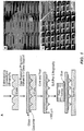
- a preferred polymer pen array ( Fig. 1 ) contains thousands of tips, preferably having a pyramidal shape, which can be made with a master prepared by conventional photolithography and subsequent wet chemical etching ( Fig. 1A ).
- the tips preferably are connected by a common substrate which includes a thin polymer backing layer (50-100 ⁇ m thick), which preferably is adhered to a rigid support (e.g., a glass, silicon, quartz, ceramic, polymer, or any combination thereof), e.g. prior to or via curing of the polymer.
- a rigid support e.g., a glass, silicon, quartz, ceramic, polymer, or any combination thereof
- the rigid support is preferably highly rigid and has a highly planar surface upon which to mount the array (e.g., silica glass, quartz, and the like).
- the rigid support and thin backing layer significantly improve the uniformity of the polymer pen array over large areas, such as three inch wafer surface ( Fig. 1B , 4 ), and make possible the leveling and uniform, controlled use of the array.
- one or more of the array tips, backing layer, and rigid support are at least translucent, and preferably transparent.
- the tip array used contained either 15,000 or 28,000 pyramid-shaped pens, but arrays with as many as about 11,000,000 pens have also been used to pattern structures ( Fig. 5 ).
- a pen array (1 cm 2 in size) was inked by immersing it in a saturated solution of 16-mercaptohexadecanoic acid (MHA) in ethanol for five minutes followed by rinsing with ethanol.
- MHA 16-mercaptohexadecanoic acid
- the inked pen array was used for generating 1- ⁇ m diameter MHA dot patterns on a thermally evaporated polycrystalline gold substrate (25 nm Au with a 5 nm Ti adhesion layer coated on Si) by bringing it in contact with the gold surface for 0.1 s. This process of contacting the gold substrate was repeated 35 times to generate a 6 ⁇ 6 array of MHA dots (less than 10% deviation in feature diameter).
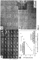
- the exposed gold on this MHA patterned substrate was subsequently etched (20 mM thiourea, 30 mM iron nitrate, 20 mM hydrochloric acid, and 2 mM octanol in water) to yield raised structures that are approximately 25 nm in height and easily imaged by optical microscopy ( Fig. 2A ).
- a defining characteristic of Polymer Pen Lithography in contrast with DPN and most contact printing strategies which are typically viewed as pressure or force-independent (21), is that it exhibits both time- and pressure-dependent ink transport.
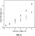
- DPN features made by Polymer Pen Lithography exhibit a size that is linearly dependent on the square root of the tip-substrate contact time ( Fig. 6 ) (27, 28).
- This property of Polymer Pen Lithography which is a result of the diffusive characteristics of the ink and the small size of the delivery tips, allows one to pattern sub-micron features with high precision and reproducibility (variation of feature size is less than 10% under the same experimental conditions).
- the pressure dependence of Polymer Pen Lithography derives from the compressible nature of the elastomer pyramid array. Indeed, the microscopic, preferably pyramidal, tips can be made to deform with successively increasing amounts of applied pressure, which can be controlled by simply extending the piezo in the vertical direction (z-piezo). Although such deformation has been regarded as a major drawback in contact printing (it can result in "roof' collapse and limit feature size resolution), with Polymer Pen Lithography, the controlled deformation can be used as an adjustable variable, allowing one to control tip-substrate contact area and resulting feature size.
- Polymer Pen Lithography unlike conventional contact printing, allows for the combinatorial patterning of molecule-based and solid-state features with dynamic control over feature size, spacing, and shape. This is accomplished by using the polymer tips to form a dot pattern of the structure one wants to make.
- a polymer pen array with 100 pyramidal tips spaced 1 mm apart was used to generate 100 duplicates of an integrated gold circuit.
- the width of each electrode in the center of the circuit is 500 nm, while the width of each electrode lead going to these nanometer scale electrodes is 10 ⁇ m, and the size of the external bonding pad is a 100 ⁇ 100 ⁇ m 2 ( Fig. 2D ).
- the circuits were divided into 35 80 ⁇ 80 ⁇ m 2 sub-patterns, which were stitched together by manually moving the stage motor after each sub-pattern was generated. This limitation could be addressed by programming the movement of the stage motor relative to the positions of the multiple sub-patterns. To accommodate both the resolution and throughput concerns, different relative z-piezo extensions at different positions of the circuit were used, where 0 (initial contact), 2, and 6 ⁇ m were used for the central electrodes, electrode leads, and bonding pads, respectively.
- Polymer Pen Lithography allows one to arbitrarily make many types of structures without the hurdle of designing a new master via a throughput-impeded serial process.
- Polymer Pen Lithography can be used with sub-100 nm resolution with the registration capabilities of a closed-loop scanner.
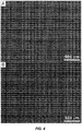
- Polymer Pen Lithography was used to generate 15,000 replicas of the 2008 Beijing Olympic logo on gold with MHA as the ink and subsequent wet chemical etching ( Fig. 3A ). Each logo was generated using the multiscale capabilities of Polymer Pen Lithography from a 70 ⁇ 60 ⁇ m 2 bitmap.
- Polymer Pen Lithography A new lithography method, termed Polymer Pen Lithography, has been developed using elastomeric pen arrays mounted on an inscripting device, such as an NscriptorTM instrument, to generate nano- and microscale features in a constructive manner.
- the technique merges many of the attributes of DPN and contact printing to yield patterning capabilities that span multiple length scales with high throughput and low cost.
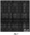
- the novel time- and pressure-dependent ink transport properties of the polymer pen pyramid arrays provide important and tunable variables that distinguish Polymer Pen Lithography from the many nano- and microfabrication approaches that have been developed to date. Since Polymer Pen Lithography is a direct-write technique, it is also useful for fabricating arrays of structures made of soft matter, such as proteins ( Fig. 7 ), making it useful in the life sciences as well.
- the lithography methods disclosed herein employ a tip array formed from elastomeric polymer material.
- the tip arrays are non-cantilevered and comprise tips which can be designed to have any shape or spacing between them, as needed.
- the shape of each tip can be the same or different from other tips of the array.
- Contemplated tip shapes include spheroid, hemispheroid, toroid, polyhedron, cone, cylinder, and pyramid (trigonal or square).
- the tips are sharp, so that they are suitable for forming submicron patterns, e.g., less than about 500 nm.
- the sharpness of the tip is measured by its radius of curvature, and the radius of curvature of the tips disclosed herein is below 1 ⁇ m, and can be less than about 0.9 ⁇ m, less than about 0.8 ⁇ m, less than about 0.7 ⁇ m, less than about 0.6 ⁇ m, less than about 0.5 ⁇ m, less than about 0.4 ⁇ m, less than about 0.3 ⁇ m, less than about 0.2 ⁇ m, less than about 0.1 ⁇ m, less than about 90 nm, less than about 80 nm, less than about 70 nm, less than about 60 nm, or less than about 50 nm.
- the tip array can be formed from a mold made using photolithography methods, which is then used to fashion the tip array using a polymer as disclosed herein.
- the mold can be engineered to contain as many tips arrayed in any fashion desired.
- the tips of the tip array can be any number desired, and contemplated numbers of tips include about 1000 tips to about 15 million tips, or greater.
- the number of tips of the tip array can be greater than about 1 million, greater than about 2 million, greater than about 3 million, greater than about 4 million, greater than 5 million tips, greater than 6 million, greater than 7 million, greater than 8 million, greater than 9 million, greater than 10 million, greater than 11 million, greater than 12 million, greater than 13 million, greater than 14 million, or greater than 15 million tips.
- the tips of the tip array can be designed to have any desired thickness, but typically the thickness of the tip array is about 50 nm to about 1 ⁇ m, about 50 nm to about 500 nm, about 50 nm to about 400 nm, about 50 nm to about 300 nm, about 50 nm to about 200 nm, or about 50 nm to about 100 nm.
- the polymers can be any polymer having a compressibility compatible with the lithographic methods.
- Polymeric materials suitable for use in the tip array can have linear or branched backbones, and can be crosslinked or non-crosslinked, depending upon the particular polymer and the degree of compressibility desired for the tip.
- Cross-linkers refer to multi-functional monomers capable of forming two or more covalent bonds between polymer molecules.
- Non-limiting examples of cross-linkers include such as trimethylolpropane trimethacrylate (TMPTMA), divinylbenzene, di-epoxies, tri-epoxies, tetra-epoxies, di-vinyl ethers, tri-vinyl ethers, tetra-vinyl ethers, and combinations thereof.
- TMPTMA trimethylolpropane trimethacrylate
- divinylbenzene divinylbenzene
- di-epoxies di-epoxies
- tri-epoxies tri-epoxies
- tetra-epoxies di-vinyl ethers
- tetra-vinyl ethers tri-vinyl ethers
- Thermoplastic or thermosetting polymers can be used, as can crosslinked elastomers.
- the polymers can be porous and/or amorphous.
- a variety of elastomeric polymeric materials are contemplated, including polymers of the general classes of silicone polymers and epoxy polymers. Polymers having low glass transition temperatures such as, for example, below 25°C or more preferably below -50°C, can be used. Diglycidyl ethers of bisphenol A can be used, in addition to compounds based on aromatic amine, triazine, and cycloaliphatic backbones. Another example includes Novolac polymers.
- elastomeric polymers include methylchlorosilanes, ethylchlorosilanes, and phenylchlorosilanes, polydimethylsiloxane (PDMS).
- PDMS polydimethylsiloxane
- Other materials include polyethylene, polystyrene, polybutadiene, polyurethane, polyisoprene, polyacrylic rubber, fluorosilicone rubber, and fluoroelastomers.
- suitable polymers that may be used to form a tip can be found in U.S. Patent No. 5,776,748 ; U.S. Patent No. 6,596,346 ; and U.S. Patent No. 6,500,549 , each of which is hereby incorporated by reference in its entirety.
- Other suitable polymers include those disclosed by He et al., Langmuir 2003, 19, 6982-6986 ; Donzel et al., Adv. Mater. 2001, 13, 1164-1167 ; and Martin et al, Langmuir, 1998, 14-15, 3791-3795 .
- Hydrophobic polymers such as polydimethylsiloxane can be modified either chemically or physically by, for example, exposure to a solution of a strong oxidizer or to an oxygen plasma.
- the polymer of the tip array has a suitable compression modulus and surface hardness to prevent collapse of the polymer during inking and printing, but too high a modulus and too great a surface hardness can lead to a brittle material that cannot adapt and conform to a substrate surface during printing.
- vinyl and hydrosilane prepolymers can be tailored to provide polymers of different modulus and surface hardness.
- the polymer is a mixture of vinyl and hydrosilane prepolymers, where the weight ratio of vinyl prepolymer to hydrosilane crosslinker is about 5:1 to about 20:1, about 7:1 to about 15:1, or about 8:1 to about 12:1.
- the polymers of the tip array preferably will have a surface hardness of about 0.2% to about 3.5% of glass, as measured by resistance of a surface to penetration by a hard sphere with a diameter of 1 mm, compared to the resistance of a glass surface (as described in Schmid, et al., Macromolecules, 33:3042 (2000 ) at p 3044).
- the surface hardness can be about 0.3% to about 3.3%, about 0.4% to about 3.2%, about 0.5% to about 3.0%, or about 0.7% to about 2.7%.
- the polymers of the tip array can have a compression modulus of about 10 MPa to about 300 MPa.
- the tip array preferably comprises a compressible polymer which is Hookean under pressures of about 10 MPa to about 300 MPa. The linear relationship between pressure exerted on the tip array and the feature size allows for control of the indicia printed using the disclosed methods and tip arrays (see Fig. 2B ).
- the tip array can comprise a polymer that has adsorption and/or absorption properties for the patterning composition, such that the tip array acts as its own patterning composition reservoir.
- PDMS is known to adsorb patterning inks, see, e.g., US Patent Publication No. 2004/228962 , Zhang, et al., Nano Lett. 4, 1649 (2004 ), and Wang et al., Langmuir 19, 8951 (2003 ).
- the tip array can comprise a plurality of tips fixed to a common substrate and formed from a polymer as disclosed herein.
- the tips can be arranged randomly or in a regular periodic pattern (e.g., in columns and rows, in a circular pattern, or the like).
- the tips can all have the same shape or be constructed to have different shapes.
- the common substrate can comprise an elastomeric layer, which can comprise the same polymer that forms the tips of the tip array, or can comprise an elastomeric polymer that is different from that of the tip array.
- the elastomeric layer can have a thickness of about 50 ⁇ m to about 100 ⁇ m.
- the tip array can be affixed or adhered to a rigid support (e.g., glass, such as a glass slide).
- the common substrate, the tip array, and/or the rigid support, if present, is translucent or transparent. In a specific case, each is translucent or transparent.
- the thickness of combination of the tip array and common substrate can be less than about 200 ⁇ m, preferably less than about 150 ⁇ m, or more preferably about 100 ⁇ m.
- Patterning compositions suitable for use in the disclosed methods include both homogeneous and heterogeneous compositions, the latter referring to a composition having more than one component.
- the patterning composition is coated on the tip array.
- coating refers both to coating of the tip array as well adsorption and absorption by the tip array of the patterning composition .
- the patterning composition can be patterned on a substrate surface using the tip array.
- Patterning compositions can be liquids, solids, semi-solids, and the like. Patterning compositions suitable for use include, but are not limited to, molecular solutions, polymer solutions, pastes, gels, creams, glues, resins, epoxies, adhesives, metal films, particulates, solders, etchants, and combinations thereof.
- Patterning compositions can include materials such as, but not limited to, monolayer-forming species, thin film-forming species, oils, colloids, metals, metal complexes, metal oxides, ceramics, organic species (e.g., moieties comprising a carbon-carbon bond, such as small molecules, polymers, polymer precursors, proteins, antibodies, and the like), polymers (e.g., both non-biological polymers and biological polymers such as single and double stranded DNA, RNA, and the like), polymer precursors, dendrimers, nanoparticles, and combinations thereof.
- materials such as, but not limited to, monolayer-forming species, thin film-forming species, oils, colloids, metals, metal complexes, metal oxides, ceramics, organic species (e.g., moieties comprising a carbon-carbon bond, such as small molecules, polymers, polymer precursors, proteins, antibodies, and the like), polymers (e.g., both non-biological polymers and biological polymers such as single and double strand
- one or more components of a patterning composition includes a functional group suitable for associating with a substrate, for example, by forming a chemical bond, by an ionic interaction, by a Van der Waals interaction, by an electrostatic interaction, by magnetism, by adhesion, and combinations thereof.
- the composition can be formulated to control its viscosity.
- Parameters that can control ink viscosity include, but are not limited to, solvent composition, solvent concentration, thickener composition, thickener concentration, particles size of a component, the molecular weight of a polymeric component, the degree of cross-linking of a polymeric component, the free volume (i.e., porosity) of a component, the swellability of a component, ionic interactions between ink components (e.g., solvent-thickener interactions), and combinations thereof.
- the patterning composition comprises an additive, such as a solvent, a thickening agent, an ionic species (e.g., a cation, an anion, a zwitterion, etc.) the concentration of which can be selected to adjust one or more of the viscosity, the dielectric constant, the conductivity, the tonicity, the density, and the like.
- an additive such as a solvent, a thickening agent, an ionic species (e.g., a cation, an anion, a zwitterion, etc.) the concentration of which can be selected to adjust one or more of the viscosity, the dielectric constant, the conductivity, the tonicity, the density, and the like.
- Suitable thickening agents include, but are not limited to, metal salts of carboxyalkylcellulose derivatives (e.g., sodium carboxymethylcellulose), alkylcellulose derivatives (e.g., methylcellulose and ethylcellulose), partially oxidized alkylcellulose derivatives (e.g., hydroxyethylcellulose, hydroxypropylcellulose and hydroxypropylmethylcellulose), starches, polyacrylamide gels, homopolymers of poly-N-vinylpyrrolidone, poly(alkyl ethers) (e.g., polyethylene oxide, polyethylene glycol, and polypropylene oxide), agar, agarose, xanthan gums, gelatin, dendrimers, colloidal silicon dioxide, lipids (e.g., fats, oils, steroids, waxes, glycerides of fatty acids, such as oleic, linoleic, linolenic, and arachidonic acid, and lipid bilayers such as from
- Suitable solvents for a patterning composition include, but are not limited to, water, C1-C8 alcohols (e.g., methanol, ethanol, propanol and butanol), C6-C12 straight chain, branched and cyclic hydrocarbons (e.g., hexane and cyclohexane), C6-C14 aryl and aralkyl hydrocarbons (e.g., benzene and toluene), C3-C10 alkyl ketones (e.g., acetone), C3-C10 esters (e.g., ethyl acetate), C4-C10 alkyl ethers, and combinations thereof.
- C1-C8 alcohols e.g., methanol, ethanol, propanol and butanol
- C6-C12 straight chain, branched and cyclic hydrocarbons e.g., hexane and cyclohexane
- a solvent is present in a concentration of about 1% to about 99%, about 5% to about 95%, about 10% to about 90%, about 15% to about 95%, about 25% to about 95%, about 50% to about 95%, or about 75% to about 95% by weight of a patterning composition.
- Patterning compositions can comprise an etchant.
- an "etchant” refers to a component that can react with a surface to remove a portion of the surface.
- an etchant is used to form a subtractive feature by reacting with a surface and forming at least one of a volatile and/or soluble material that can be removed from the substrate, or a residue, particulate, or fragment that can be removed from the substrate by, for example, a rinsing or cleaning method.
- an etchant is present in a concentration of about 0.5% to about 95%, about 1% to about 90%, about 2% to about 85%, about 0.5% to about 10%, or about 1% to about 10% by weight of the patterning composition.
- Etchants suitable for use in the methods disclosed herein include, but are not limited to, an acidic etchant, a basic etchant, a fluoride-based etchant, and combinations thereof.
- Acidic etchants suitable for use with the present invention include, but are not limited to, sulfuric acid, trifluoromethanesulfonic acid, fluorosulfonic acid, trifluoroacetic acid, hydrofluoric acid, hydrochloric acid, carborane acid, and combinations thereof.
- Basic etchants suitable for use with the present invention include, but are not limited to, sodium hydroxide, potassium hydroxide, ammonium hydroxide, tetraalkylammonium hydroxide ammonia, ethanolamine, ethylenediamine, and combinations thereof.
- Fluoride-based etchants suitable for use with the present invention include, but are not limited to, ammonium fluoride, lithium fluoride, sodium fluoride, potassium fluoride, rubidium fluoride, cesium fluoride, francium fluoride, antimony fluoride, calcium fluoride, ammonium tetrafluoroborate, potassium tetrafluoroborate, and combinations thereof.
- the patterning composition includes a reactive component.
- a reactive component refers to a compound or species that has a chemical interaction with a substrate.
- a reactive component in the ink penetrates or diffuses into the substrate.
- a reactive component transforms, binds, or promotes binding to exposed functional groups on the surface of the substrate.
- Reactive components can include, but are not limited to, ions, free radicals, metals, acids, bases, metal salts, organic reagents, and combinations thereof.
- Reactive components further include, without limitation, monolayer-forming species such as thiols, hydroxides, amines, silanols, siloxanes, and the like, and other monolayer-forming species known to a person or ordinary skill in the art.
- monolayer-forming species such as thiols, hydroxides, amines, silanols, siloxanes, and the like, and other monolayer-forming species known to a person or ordinary skill in the art.
- the reactive component can be present in a concentration of about 0.001 % to about 100%, about 0.001% to about 50%, about 0.001% to about 25%, about 0.001% to about 10%, about 0.001% to about 5%, about 0.001% to about 2%, about 0.001% to about 1%, about 0.001% to about 0.5%, about 0.001% to about 0.05%, about 0.01% to about 10%, about 0.01% to about 5%, about 0.01% to about 2%, about 0.01% to about 1 %, about 10% to about 100%, about 50% to about 99%, about 70% to about 95%, about 80% to about 99%, about 0.001%, about 0.005%, about 0.01%, about 0.1%, about 0.5%, about 1%, about 2%, or about 5% weight of the patterning composition.
- the patterning composition can further comprise a conductive and/or semi-conductive component.
- a "conductive component” refers to a compound or species that can transfer or move electrical charge.
- Conductive and semi-conductive components include, but are not limited to, a metal, a nanoparticle, a polymer, a cream solder, a resin, and combinations thereof.
- a conductive component is present in a concentration of about 1% to about 100%, about 1% to about 10%, about 5% to about 100%, about 25% to about 100%, about 50% to about 100%, about 75% to about 99%, about 2%, about 5%, about 90%, about 95% by weight of the patterning composition.
- Metals suitable for use in a patterning composition include, but are not limited to, a transition metal, aluminum, silicon, phosphorous, gallium, germanium, indium, tin, antimony, lead, bismuth, alloys thereof, and combinations thereof.
- the patterning composition comprises a semi-conductive polymer.
- Semi-conductive polymers suitable for use with the present invention include, but are not limited to, a polyaniline, a poly(3,4-ethylenedioxythiophene)-poly(styrenesulfonate), a polypyrrole, an arylene vinylene polymer, a polyphenylenevinylene, a polyacetylene, a polythiophene, a polyimidazole, and combinations thereof.
- the patterning composition can include an insulating component.
- an "insulating component” refers to a compound or species that is resistant to the movement or transfer of electrical charge.
- an insulating component has a dielectric constant of about 1.5 to about 8 about 1.7 to about 5, about 1.8 to about 4, about 1.9 to about 3, about 2 to about 2.7, about 2.1 to about 2.5, about 8 to about 90, about 15 to about 85, about 20 to about 80, about 25 to about 75, or about 30 to about 70.
- Insulating components suitable for use in the methods disclosed herein include, but are not limited to, a polymer, a metal oxide, a metal carbide, a metal nitride, monomeric precursors thereof, particles thereof, and combinations thereof.
- Suitable polymers include, but are not limited to, a polydimethylsiloxane, a silsesquioxane, a polyethylene, a polypropylene, a polyimide, and combinations thereof.
- an insulating component is present in a concentration of about 1% to about 95%, about 1% to about 80%, about 1% to about 50%, about 1% to about 20%, about 1% to about 10%, about 20% to about 95%, about 20% to about 90%, about 40% to about 80%, about 1%, about 5%, about 10%, about 90%, or about 95% by weight of the patterning composition.
- the patterning composition can include a masking component.
- a “masking component” refers to a compound or species that upon reacting forms a surface feature resistant to a species capable of reacting with the surrounding surface.
- Masking components suitable for use with the present invention include materials commonly employed in traditional photolithography methods as "resists" (e.g., photoresists, chemical resists, self-assembled monolayers, etc.).
- Masking components suitable for use in the disclosed methods include, but are not limited to, a polymer such as a polyvinylpyrollidone, poly(epichlorohydrin-co-ethyleneoxide), a polystyrene, a poly(styrene-co-butadiene), a poly(4-vinylpyridine-co-styrene), an amine terminated poly(styrene-co-butadiene), a poly(acrylonitrile-co-butadiene), a styrene-butadiene-styrene block copolymer, a styrene-ethylene-butylene block linear copolymer, a polystyrene-block-poly(ethylene-ran-butylene)-block-polystyrene, a poly(styrene-co-maleic anhydride), a polystyrene-block-poly(ethylene-ran-butylene)-block
- the patterning composition can include a conductive component and a reactive component.
- a reactive component can promote at least one of: penetration of a conductive component into a surface, reaction between the conductive component and a surface, adhesion between a conductive feature and a surface, promoting electrical contact between a conductive feature and a surface, and combinations thereof.
- Surface features formed by reacting this patterning composition include conductive features selected from the group consisting of: additive non-penetrating, additive penetrating, subtractive penetrating, and conformal penetrating surface features.
- the patterning composition can comprise an etchant and a conductive component, for example, suitable for producing a subtractive surface feature having a conductive feature inset therein.
- the patterning composition can comprise an insulating component and a reactive component.
- a reactive component can promote at least one of: penetration of an insulating component into a surface, reaction between the insulating component and a surface, adhesion between an insulating feature and a surface, promoting electrical contact between an insulating feature and a surface, and combinations thereof.
- Surface features formed by reacting this patterning composition include insulating features selected from the group consisting of: additive non-penetrating, additive penetrating, subtractive penetrating, and conformal penetrating surface features.
- the patterning composition can comprise an etchant and an insulating component, for example, suitable for producing a subtractive surface feature having an insulating feature inset therein.
- the patterning composition can comprise a conductive component and a masking component, for example, suitable for producing electrically conductive masking features on a surface.
- thiols 1,9-Nonanedithiol solution
- silane silazanes
- alkynes cystamine N-Fmoc protected amino thiols
- biomolecules DNA, proteins, antibodies, collagen, peptides, biotin, and carbon nanotubes.
- Substrates suitable for use in methods disclosed herein include, but are not limited to, metals, alloys, composites, crystalline materials, amorphous materials, conductors, semiconductors, optics, fibers, inorganic materials, glasses, ceramics (e.g., metal oxides, metal nitrides, metal silicides, and combinations thereof), zeolites, polymers, plastics, organic materials, minerals, biomaterials, living tissue, bone, films thereof, thin films thereof, laminates thereof, foils thereof, composites thereof, and combinations thereof.
- ceramics e.g., metal oxides, metal nitrides, metal silicides, and combinations thereof
- zeolites e.g., polymers, plastics, organic materials, minerals, biomaterials, living tissue, bone, films thereof, thin films thereof, laminates thereof, foils thereof, composites thereof, and combinations thereof.
- a substrate can comprise a semiconductor such as, but not limited to: crystalline silicon, polycrystalline silicon, amorphous silicon, p-doped silicon, n-doped silicon, silicon oxide, silicon germanium, germanium, gallium arsenide, gallium arsenide phosphide, indium tin oxide, and combinations thereof.
- a substrate can comprise a glass such as, but not limited to, undoped silica glass (SiO 2 ), fluorinated silica glass, borosilicate glass, borophosphorosilicate glass, organosilicate glass, porous organosilicate glass, and combinations thereof.
- the substrate can be a non-planar substrate, such as pyrolytic carbon, reinforced carbon-carbon composite, a carbon phenolic resin, and the like, and combinations thereof.
- a substrate can comprise a ceramic such as, but not limited to, silicon carbide, hydrogenated silicon carbide, silicon nitride, silicon carbonitride, silicon oxynitride, silicon oxycarbide, high-temperature reusable surface insulation, fibrous refractory composite insulation tiles, toughened unipiece fibrous insulation, low-temperature reusable surface insulation, advanced reusable surface insulation, and combinations thereof.
- a substrate can comprise a flexible material, such as, but not limited to: a plastic, a metal, a composite thereof, a laminate thereof, a thin film thereof, a foil thereof, and combinations thereof.
- the disclosed methods provide the ability for in situ imaging capabilities, similar to scanning probe microscope-based lithography methods (e.g., dip pen lithography) as well as the ability to pattern a feature in a fast fashion, similar to micro-contact printing.
- the features that can be patterned range from sub-100 nm to 1 mm in size or greater, and can be controlled by altering the contacting time and/or the contacting pressure of the tip array.
- the amount of patterning composition (as measured by feature size) deposited onto a substrate surface is proportional to the contacting time, specifically a square root correlation with contacting time, see Fig. 6 .
- the contacting pressure of the tip array can be used to modify the amount of patterning composition that can be deposited onto the substrate surface.
- the pressure of the contact can be controlled by the z-piezo of a piezo scanner, see Fig. 2B .
- the more pressure (or force) exerted on the tip array the larger the feature size.
- any combination of contacting time and contacting force/pressure can provide a means for the formation of a feature size from about 30 nm to about 1 mm or greater.
- the ability to prepare features of such a wide range of sizes and in a "direct writing" or in situ manner in milliseconds makes the disclosed lithography method adaptable to a host of lithography applications, including electronics (e.g., patterning circuits) and biotechnology (e.g., arraying targets for biological assays).
- the contacting pressure of the tip array can be about 10 MPa to about 300 MPa.
- the feature size of the resulting indicia is independent of the contacting pressure, which allows for one to level the tip array on the substrate surface without changing the feature size of the indicia.
- Such low pressures are achievable by 0.5 ⁇ m or less extensions of the z-piezo of a piezo scanner to which a tip array is mounted, and pressures of about 0.01 g/cm 2 to about 0.1 g/cm 2 can be applied by z-piezo extensions of less than 0.5 ⁇ m.
- This "buffering" pressure range allows one to manipulate the tip array, substrate, or both to make initial contact between tips and substrate surface without compressing the tips, and then using the degree of compression of tips (observed by changes in reflection of light off the inside surfaces of the tips) to achieve a uniform degree of contact between tips and substrate surface.
- This leveling ability is important, as non-uniform contact of the tips of the tip array can lead to non-uniform indicia. Given the large number of tips of the tip array (e.g., 11 million in an example provided herein) and their small size, as a practical matter it may be difficult or impossible to know definitively if all of the tips are in contact with the surface.
- a defect in a tip or the substrate surface, or an irregularity in a substrate surface may result in a single tip not making contact while all other tips are in uniform contact.
- the disclosed methods provide for at least substantially all of the tips to be in contact with the substrate surface (e.g., to the extent detectable). For example, at least 90%, at least 95%, at least 96%, at least 97%, at least 98%, or at least 99% of the tips will be in contact with the substrate surface.
- the leveling of the tip array and substrate surface with respect to one another is be assisted by the fact that with a transparent, or at least translucent, tip array and common substrate arrangement, one can observe the change in reflection of light that is directed from the top of the tip array (i.e., behind the base of the tips and common substrate) through to the substrate surface.
- the intensity of light reflected from the tips of the tip array gets greater upon contact with the substrate surface (e.g., the internal surfaces of the tip array reflect light differently upon contact).
- the tip array and/or the substrate surface are translucent or transparent to allow for observing the change in light reflection of the tips upon contact with the substrate surface.
- any rigid backing material to which the tip array is mounted is also preferably at least transparent or translucent.
- the contacting time for the tips can be from about 0.001 s to about 60 s, depending upon the amount of patterning composition desired in any specific point on a substrate surface.
- the contacting force can be controlled by altering the z-piezo of the piezo scanner or by other means that allow for controlled application of force across the tip array.
- the substrate surface can be contacted with a tip array a plurality of times, wherein the tip array, the substrate surface or both move to allow for different portions of the substrate surface to be contacted.
- the time and pressure of each contacting step can be the same or different, depending upon the desired pattern.
- the shape of the indicia or patterns has no practical limitation, and can include dots, lines (e.g., straight or curved, formed from individual dots or continuously), a preselected pattern, or any combination thereof.
- the indicia resulting from the disclosed methods have a high degree of sameness, and thus are uniform or substantially uniform in size, and preferably also in shape.
- the individual indicia feature size (e.g., a dot or line width) is highly uniform, for example within a tolerance of about 5%, or about 1%, or about 0.5%.
- the tolerance can be about 0.9%, about 0.8%, about 0.7%, about 0.6%, about 0.4%, about 0.3%, about 0.2%, or about 0.1%.
- Nonuniformity of feature size and/or shape can lead to roughness of indicia that can be undesirable for sub-micron type patterning.
- the feature size can be about 10 nm to about 1 mm, about 10 nm to about 500 ⁇ m, about 10 nm to about 100 ⁇ m, about 50 nm to about 100 ⁇ m, about 50 nm to about 50 ⁇ m, about 50 nm to about 10 ⁇ m, about 50 nm to about 5 ⁇ m, or about 50 nm to about 1 ⁇ m.
- Features sizes can be less than 1 ⁇ m, less than about 900 nm, less than about 800 nm, less than about 700 nm, less than about 600 nm, less than about 500 nm, less than about 400 nm, less than about 300 nm, less than about 200 nm, less than about 100 nm, or less than about 90 nm.
- Shipley1805 (MicroChem, Inc.) photoresist was spin-coated onto gold thin film substrates (10 nm Cr adhesion layer with 100 nm of Au thermally evaporated on a precleaned oxidized Si ⁇ 100> wafer). Square well arrays were fabricated by photolithography using a chrome mask. The photoresist patterns were developed in an MF319 developing solution (MicroChem, Inc.), and then exposed to O 2 plasma for 30 s (200 mTorr) to remove the residual organic layer. Subsequently, the substrates were placed in gold (Type TFA, Transene) and chromium (Type 1020, Transene) etching solutions, respectively.
- gold Type TFA, Transene
- chromium Type 1020, Transene
- Copious rinsing with MiliQ water was required after each etching step to clean the surface.
- the photoresist was then washed away with acetone to expose the gold pattern.
- the gold patterned substrate was placed in a KOH etching solution (30% KOH in H 2 O:IPA (4:1 v/v)) at 75°C for ⁇ 25 min with vigorous stirring.
- the uncovered areas of the Si wafer were etched anisotropically, resulting in the formation of recessed pyramids.
- the remaining Au and Cr layers were removed by wet chemical etching.
- the pyramid master was modified with 1H,1H,2H,2H-perfluorodecyltrichlorosilane (Gelest, Inc.) by gas phase silanization.
- Hard PDMS ( h -PDMS) (1,2) was used for fabricating the polymer pen arrays.
- the h -PDMS was composed of 3.4 g of vinyl-compound-rich prepolymer (VDT-731, Gelest) and 1.0 g of hydrosilane-rich crosslinker (HMS-301).
- Preparation of polymers typically required the addition of 20 ppm w/w platinum catalyst to the vinyl fraction (platinumdivinyltetramethyldisiloxane complex in xylene, SIP 6831.1 Gelest) and 0.1% w/w modulator to the mixture (2,4,6,8-tetramethyltetravinylcyclotetrasiloxane, Fluka).
- Tetramethylrhodamine 5-(and-6)-isothiocyanate (TRITC) conjugated anti-mouse IgG arrays were generated on a CodelinkTM glass slide (GE Healthcare) by Polymer Pen Lithography.
- the polymer pen array was modified with polyethylene glycol silane (PEG-silane) to minimize non-specific interactions between the protein and PDMS surface.
- PEG-silane polyethylene glycol silane
- the polymer pen array was briefly exposed to an oxygen plasma (30 sec) to render the surface hydrophilic.
- Fig. 7 shows the fluorescent image of the as generated 3 ⁇ 3 IgG arrays. Each IgG dot was made by contacting the tip array with the substrate for 3 seconds. The size of each IgG dot was 4 ⁇ 0.7 ⁇ m.
Landscapes
- Engineering & Computer Science (AREA)
- Chemical & Material Sciences (AREA)
- Nanotechnology (AREA)
- Physics & Mathematics (AREA)
- General Physics & Mathematics (AREA)
- Crystallography & Structural Chemistry (AREA)
- Manufacturing & Machinery (AREA)
- Mechanical Engineering (AREA)
- Mathematical Physics (AREA)
- Condensed Matter Physics & Semiconductors (AREA)
- Theoretical Computer Science (AREA)
- Micromachines (AREA)
- Exposure Of Semiconductors, Excluding Electron Or Ion Beam Exposure (AREA)
Claims (16)
- Verfahren zum Drucken von Zeichen im Submikrometerbereich auf einer Substratoberfläche, das Folgendes umfasst:Beschichten einer Spitzenanordnung mit einer Strukturierungszusammensetzung, wobei die Spitzenanordnung ein komprimierbares Elastomer-Polymer umfasst, das mehrere Spitzen ohne Biegebalken umfasst, die jeweils einen Krümmungsradius von weniger als etwa 1 µm aufweisen, und ein gemeinsames Substrat, das eine Elastomerschicht umfasst, die ein komprimierbares Elastomer-Polymer umfasst, wobei die Spitzenanordnung und das gemeinsame Substrat auf einem starren Träger fixiert sind und die Spitzenanordnung, das gemeinsame Substrat und der starre Träger gemeinsam wenigstens durchscheinend sind;Kontaktieren der Substratoberfläche für eine erste Kontaktzeitperiode und bei einem ersten Kontaktdruck mit allen oder im Wesentlichen allen der beschichteten Spitzen der Anordnung, um die Strukturierungszusammensetzung auf die Substratoberfläche abzuscheiden und im Wesentlichen gleichmäßige Zeichen mit allen oder im Wesentlichen allen der beschichteten Spitzen zu bilden, wobei die Zeichen eine Punktgröße oder eine Linienbreite von weniger als 1 µm aufweisen.
- Verfahren nach Anspruch 1, wobei die Spitzenanordnung mehrere Spitzen umfasst, die in einem regelmäßigen periodischen Muster angeordnet sind.
- Verfahren nach Anspruch 1 und 2, wobei jede Spitze einen Krümmungsradius von weniger als etwa 0,2 µm aufweist.
- Verfahren nach einem der Ansprüche 1-3, wobei das Polymer einen Kompressionsmodul von etwa 10 MPa bis etwa 300 MPa aufweist.
- Verfahren nach einem der Ansprüche 1-4, wobei das Polymer Polydimethylsiloxan (PDMS) umfasst.
- Verfahren nach Anspruch 5, wobei das PDMS ein trimethylsiloxan-terminiertes Vinylmethylsiloxandimethylsiloxan-Copolymer, ein Methylhydrosiloxandimethylsiloxan-Copolymer oder eine Mischung davon umfasst.
- Verfahren nach einem der Ansprüche 1-6, wobei jede Spitze der Spitzenanordnung identisch geformt ist.
- Verfahren nach einem der Ansprüche 1-7, das ferner Bewegen der Spitzenanordnung, der Substratoberfläche oder von beiden und Wiederholen des Kontaktierungsschrittes für eine zweite Kontaktzeitperiode und bei einem zweiten Kontaktdruck umfasst.
- Verfahren nach einem der Ansprüche 1-8, das Begrenzen einer lateralen Bewegung zwischen der Spitzenanordnung und dem Substrat zum Bilden von Zeichen, die Punkte umfassen, umfasst.
- Verfahren nach Anspruch 9, das Steuern der Kontaktzeitperiode, des Kontaktdrucks oder von beiden umfasst, um die Punkte mit einem Durchmesser in einem Bereich von etwa 10 nm bis etwa 500 µm zu bilden.
- Verfahren nach einem der Ansprüche 1-8, das Steuern einer lateralen Bewegung zwischen der Spitzenanordnung und der Substratoberfläche während des Kontaktierens und/oder zwischen einem oder mehreren Sätzen von Kontaktierungs- und Abscheidungsschritten zum Bilden von Zeichen, die Linien und/oder ein vorausgewähltes Muster umfassen, umfasst.
- Verfahren nach einem der Ansprüche 1-11, das Auswählen eines komprimierbaren Polymers für die Spitzenanordnung umfasst, welches unter Drücken von 10 MPa bis 300 MPa dem Hookeschen Gesetz folgt.
- Verfahren nach einem der Ansprüche 1-11, wobei die Zeichen eine Punktgröße oder eine Linienbreite von weniger als 100 nm aufweisen.
- Verfahren nach einem der Ansprüche 1-11 und 13, das ferner Nivellieren der Spitzen der Spitzenanordnung mit Bezug auf die Substratoberfläche durch Folgendes umfasst:Hinterleuchten der Spitzenanordnung mit einfallendem Licht, um eine interne Reflexion des einfallenden Lichts von den internen Oberflächen der Spitzen zu bewirken;Zusammenbringen der Spitzen der Spitzenanordnung und der Substratoberfläche entlang einer Z-Achse bis zu einem Kontaktpunkt zwischen einem Teilsatz der Spitzen mit der Substratoberfläche, wobei ein Kontakt durch eine erhöhte Intensität von reflektiertem Licht von dem Teilsatz der Spitzen in Kontakt mit der Substratoberfläche angegeben wird, wohingegen keine Änderung der Intensität von reflektiertem Licht von anderen Spitzen nichtkontaktierende Spitzen angibt; undNeigen der Spitzenanordnung und/oder der Substratoberfläche mit Bezug aufeinander als Reaktion auf Unterschiede der Intensität des reflektierten Lichts von den internen Oberflächen der Spitzen, um einen Kontakt zwischen der Substratoberfläche und nichtkontaktierenden Spitzen zu erzielen, wobei das Neigen ein- oder mehrmals entlang einer X-, Y- und/oder Z-Achse durchgeführt wird.
- Verfahren nach einem der Ansprüche 1-11 und 13, das ferner Nivellieren der Spitzen der Spitzenanordnung mit Bezug auf die Substratoberfläche durch Folgendes umfasst:Hinterleuchten der Spitzenanordnung mit einfallendem Licht, um eine interne Reflexion des einfallenden Lichts von den internen Oberflächen der Spitzen zu bewirken;Zusammenbringen der Spitzen der Spitzenanordnung und der Substratoberfläche entlang einer Z-Achse, um einen Kontakt zwischen den Spitzen der Spitzenanordnung und der Substratoberfläche zu bewirken;weiteres Bewegen der Spitzenanordnung und/oder des Substrats zueinander entlang der Z-Achse, um einen Teilsatz der Spitzen zu komprimieren, wobei die Intensität des reflektierten Lichts von den Spitzen als eine Funktion des Kompressionsgrades der Spitzen gegen die Substratoberfläche zunimmt; undNeigen der Spitzenanordnung und/oder der Substratoberfläche mit Bezug aufeinander als Reaktion auf Unterschiede der Intensität des reflektierten Lichts von internen Oberflächen der Spitzen, um einen im Wesentlichen gleichmäßigen Kontakt zwischen der Substratoberfläche und den Spitzen zu erzielen, wobei das Neigen ein- oder mehrmals entlang einer X-, Y- und/oder Z-Achse durchgeführt wird.
- Spitzenanordnung, die mehrere identisch geformte Spitzen ohne Biegebalken umfasst, die auf einem gemeinsamen Substrat fixiert sind, wobei die Spitzen und das gemeinsame Substrat aus einem Elastomer-Polymer gebildet sind, das Elastomer-Polymer der Spitzen einen Kompressionsmodul von etwa 10 MPa bis etwa 300 MPa aufweist und jede Spitze einen Krümmungsradius von weniger als etwa 1 µm aufweist, dadurch gekennzeichnet, dass das gemeinsame Substrat auf einem starren Träger fixiert ist und die Spitzenanordnung, das gemeinsame Substrat und der starre Träger wenigstens durchscheinend sind.
Applications Claiming Priority (4)
| Application Number | Priority Date | Filing Date | Title |
|---|---|---|---|
| US4791008P | 2008-04-25 | 2008-04-25 | |
| US4967908P | 2008-05-01 | 2008-05-01 | |
| US7619908P | 2008-06-27 | 2008-06-27 | |
| PCT/US2009/041738 WO2009132321A1 (en) | 2008-04-25 | 2009-04-25 | Polymer pen lithography |
Publications (3)
| Publication Number | Publication Date |
|---|---|
| EP2283395A1 EP2283395A1 (de) | 2011-02-16 |
| EP2283395A4 EP2283395A4 (de) | 2014-07-09 |
| EP2283395B1 true EP2283395B1 (de) | 2018-08-22 |
Family
ID=41217168
Family Applications (1)
| Application Number | Title | Priority Date | Filing Date |
|---|---|---|---|
| EP09735282.7A Active EP2283395B1 (de) | 2008-04-25 | 2009-04-25 | Polymer-stift-lithographie |
Country Status (7)
| Country | Link |
|---|---|
| US (3) | US9372397B2 (de) |
| EP (1) | EP2283395B1 (de) |
| JP (1) | JP2011519168A (de) |
| KR (1) | KR20110014606A (de) |
| CN (1) | CN102037407B (de) |
| ES (1) | ES2687650T3 (de) |
| WO (1) | WO2009132321A1 (de) |
Families Citing this family (46)
| Publication number | Priority date | Publication date | Assignee | Title |
|---|---|---|---|---|
| US8159825B1 (en) | 2006-08-25 | 2012-04-17 | Hypres Inc. | Method for fabrication of electrical contacts to superconducting circuits |
| ES2687650T3 (es) | 2008-04-25 | 2018-10-26 | Northwestern University | Litografía de Plumas de Polímero |
| US20100143666A1 (en) | 2008-11-20 | 2010-06-10 | Northwestern University | Redox activated patterning |
| SG172852A1 (en) | 2009-01-26 | 2011-08-29 | Nanoink Inc | Large area, homogeneous array fabrication including homogeneous substrates |
| WO2010085767A1 (en) | 2009-01-26 | 2010-07-29 | Nanoink. Inc. | Large area, homogeneous array fabrication including controlled tip loading vapor deposition |
| US8214916B2 (en) | 2009-01-26 | 2012-07-03 | Nanoink, Inc. | Large area, homogeneous array fabrication including leveling with use of bright spots |
| CA2758530A1 (en) * | 2009-04-24 | 2010-10-28 | Northwestern University | Multiplexed biomolecule arrays made by polymer pen lithography |
| US8961853B2 (en) * | 2009-06-05 | 2015-02-24 | Northwestern University | Silicon pen nanolithography |
| WO2011017487A2 (en) * | 2009-08-05 | 2011-02-10 | Cornell University | Methods and apparatus for high-throughput formation of nano-scale arrays |
| WO2011068960A2 (en) * | 2009-12-02 | 2011-06-09 | Northwestern University | Block copolymer-assisted nanolithography |
| WO2011071753A2 (en) | 2009-12-07 | 2011-06-16 | Northwestern University | Generation of combinatorial patterns by deliberate tilting of a polymer-pen array |
| US8745761B2 (en) * | 2009-12-07 | 2014-06-03 | Northwestern University | Force feedback leveling of tip arrays for nanolithography |
| US20110274839A1 (en) | 2010-04-14 | 2011-11-10 | Nanoink, Inc. | Cantilevers for deposition |
| US20110277193A1 (en) | 2010-04-20 | 2011-11-10 | Nanolnk, Inc. | Sensors and biosensors |
| WO2012026927A1 (en) | 2010-08-24 | 2012-03-01 | Nanoink, Inc. | Leveling devices and methods |
| DE202010013706U1 (de) | 2010-09-28 | 2011-03-24 | NANOINK, INC., Skokie | Einrichtung zur Nivellierung |
| WO2012047808A1 (en) | 2010-10-07 | 2012-04-12 | Nanoink, Inc. | Cell assay methods and articles |
| WO2012061308A1 (en) | 2010-11-01 | 2012-05-10 | Nanoink, Inc. | High-throughput assay methods and articles |
| WO2012061314A1 (en) | 2010-11-01 | 2012-05-10 | Nanoink, Inc. | High-throughput slide processing apparatus |
| US20140038849A1 (en) * | 2011-03-17 | 2014-02-06 | Northwestern University | Method of analyzing an analyte using combinatorial arrays and uniform patterns |
| US20120309647A1 (en) | 2011-05-31 | 2012-12-06 | Nanolnk, Inc. | Patterning and cellular co-culture |
| WO2013002858A1 (en) * | 2011-06-27 | 2013-01-03 | New York University | Nanoreactor printing |
| WO2013119845A1 (en) | 2012-02-07 | 2013-08-15 | Vibrant Holdings, Llc | Substrates, peptide arrays, and methods |
| US9079338B2 (en) | 2012-05-09 | 2015-07-14 | The Hong Kong Polytechnic University | Composite tip array for polymer pen lithography |
| US10006909B2 (en) | 2012-09-28 | 2018-06-26 | Vibrant Holdings, Llc | Methods, systems, and arrays for biomolecular analysis |
| CA3088591C (en) * | 2012-09-28 | 2023-01-03 | Vibrant Holdings, Llc | Inverted pillar plates for assaying microarrays and methods of using same. |
| CN104903793A (zh) * | 2012-10-29 | 2015-09-09 | 西北大学 | 热启动和投影平版印刷系统和方法 |
| US10286376B2 (en) | 2012-11-14 | 2019-05-14 | Vibrant Holdings, Llc | Substrates, systems, and methods for array synthesis and biomolecular analysis |
| US9618840B2 (en) * | 2012-11-20 | 2017-04-11 | New York University | Systems and methods for polymer tips using silanated supports |
| EP2956771B1 (de) | 2013-02-15 | 2020-04-08 | Vibrant Holdings, LLC | Verfahren und zusammensetzungen für verstärkte elektrochemilumineszenzdetektion |
| ES2555790B1 (es) | 2014-06-05 | 2016-10-13 | Consejo Superior De Investigaciones Científicas (Csic) | Método de obtención de un array de micropartículas planares con multiplexado molecular superficial, array obtenido y su uso |
| CN107923928B (zh) * | 2015-05-19 | 2020-07-17 | 南洋理工大学 | 检查样品表面的装置和方法 |
| US9971239B2 (en) | 2015-10-22 | 2018-05-15 | Northwestern University | Silica polymer pen lithography |
| CN107175939B (zh) * | 2016-03-09 | 2020-02-28 | 华邦电子股份有限公司 | 用于印刷线路制程的印章及其制造方法以及印刷线路制程 |
| WO2017210298A1 (en) | 2016-05-31 | 2017-12-07 | Northwestern University | Method for the fabrication of three-dimensional objects and apparatus for same |
| US10563244B2 (en) | 2016-09-20 | 2020-02-18 | Northwestern University | Nanopatterned extracellular matrices enable cell-based assays with a mass spectrometric readout |
| US10752794B2 (en) | 2016-11-18 | 2020-08-25 | Saint Louis University | Mask free methods of depositing compositions to form heterostructures |
| EP3552027B1 (de) | 2016-12-07 | 2023-05-03 | Northwestern University | Flüssige masken für mikrofertigungsverfahren |
| WO2018218250A2 (en) | 2017-05-26 | 2018-11-29 | Vibrant Holdings, Llc | Photoactive compounds and methods for biomolecule detection and sequencing |
| EP3631688A4 (de) * | 2017-06-02 | 2021-03-31 | Tera-print, LLC | Herstellung von mikro-/nanoskaligen barcodes unter verwendung von trägerfreier rastersondenlithografie |
| CN113982549A (zh) | 2017-07-20 | 2022-01-28 | 沙特阿拉伯石油公司 | 通过使用表面改性减轻凝析物堆积 |
| EP3790985B1 (de) | 2018-05-09 | 2026-04-15 | Vibrant Holdings, LLC | Verfahren zur synthese eines polynukleotidarrays unter verwendung von fotootaktivierten mitteln |
| WO2020154063A1 (en) | 2019-01-23 | 2020-07-30 | Saudi Arabian Oil Company | Mitigation of condensate and water banking using functionalized nanoparticles |
| CN118636467A (zh) | 2019-03-07 | 2024-09-13 | 西北大学 | 形成三维物体的方法和形成三维物体的设备 |
| KR20220110496A (ko) * | 2019-12-06 | 2022-08-08 | 노오쓰웨스턴 유니버시티 | 할로겐화물 페로브스카이트 나노결정 어레이 및 이의 제조 방법 |
| TWI752844B (zh) * | 2021-03-10 | 2022-01-11 | 光群雷射科技股份有限公司 | 轉印滾輪及其製造方法 |
Family Cites Families (30)
| Publication number | Priority date | Publication date | Assignee | Title |
|---|---|---|---|---|
| US5472881A (en) | 1992-11-12 | 1995-12-05 | University Of Utah Research Foundation | Thiol labeling of DNA for attachment to gold surfaces |
| US5776748A (en) | 1993-10-04 | 1998-07-07 | President And Fellows Of Harvard College | Method of formation of microstamped patterns on plates for adhesion of cells and other biological materials, devices and uses therefor |
| US6339217B1 (en) * | 1995-07-28 | 2002-01-15 | General Nanotechnology Llc | Scanning probe microscope assembly and method for making spectrophotometric, near-field, and scanning probe measurements |
| US5846909A (en) | 1995-05-22 | 1998-12-08 | University Of Texas System | Molecular level, precision control over the interfacial properties of high-TC superconductor structures and devices |
| DE69524247T2 (de) * | 1995-08-04 | 2002-08-08 | International Business Machines Corp., Armonk | Stempel für lithographie-verfahren |
| US5942397A (en) | 1996-12-11 | 1999-08-24 | Tarlov; Michael J. | Surface immobilization of biopolymers |
| US5908692A (en) | 1997-01-23 | 1999-06-01 | Wisconsin Alumni Research Foundation | Ordered organic monolayers and methods of preparation thereof |
| US6304364B1 (en) * | 1997-06-11 | 2001-10-16 | President & Fellows Of Harvard College | Elastomeric light valves |
| WO1999048682A1 (en) | 1998-03-27 | 1999-09-30 | University Of Pittsburgh | Tarnish resistant article, preparation, manufacture and methods of use of same |
| ES2308853T3 (es) | 1998-10-13 | 2008-12-01 | Gambro Lundia Ab | Pelicula de polimero biocompatible. |
| US6635311B1 (en) | 1999-01-07 | 2003-10-21 | Northwestern University | Methods utilizing scanning probe microscope tips and products therefor or products thereby |
| US6827979B2 (en) * | 1999-01-07 | 2004-12-07 | Northwestern University | Methods utilizing scanning probe microscope tips and products therefor or produced thereby |
| US6596346B2 (en) | 2000-09-29 | 2003-07-22 | International Business Machines Corporation | Silicone elastomer stamp with hydrophilic surfaces and method of making same |
| US7265188B2 (en) * | 2000-10-06 | 2007-09-04 | The Procter & Gamble Company | Biodegradable polyester blend compositions and methods of making the same |
| US7491422B2 (en) | 2002-10-21 | 2009-02-17 | Nanoink, Inc. | Direct-write nanolithography method of transporting ink with an elastomeric polymer coated nanoscopic tip to form a structure having internal hollows on a substrate |
| US7034854B2 (en) | 2002-11-12 | 2006-04-25 | Nanoink, Inc. | Methods and apparatus for ink delivery to nanolithographic probe systems |
| US20040228962A1 (en) | 2003-05-16 | 2004-11-18 | Chang Liu | Scanning probe microscopy probe and method for scanning probe contact printing |
| US7690325B2 (en) | 2004-04-30 | 2010-04-06 | Bioforce Nanosciences, Inc. | Method and apparatus for depositing material onto a surface |
| KR101368748B1 (ko) * | 2004-06-04 | 2014-03-05 | 더 보오드 오브 트러스티스 오브 더 유니버시티 오브 일리노이즈 | 인쇄가능한 반도체소자들의 제조 및 조립방법과 장치 |
| KR101200341B1 (ko) * | 2004-08-25 | 2012-11-12 | 미쓰이 가가쿠 가부시키가이샤 | 수지 조성물 및 이것으로부터 얻어지는 필름 |
| US20070269747A1 (en) | 2004-09-13 | 2007-11-22 | Maneesh Bahadur | Lithography Technique Using Silicone Molds |
| WO2007081876A2 (en) * | 2006-01-04 | 2007-07-19 | Liquidia Technologies, Inc. | Nanostructured surfaces for biomedical/biomaterial applications and processes thereof |
| JP2007245684A (ja) * | 2006-03-20 | 2007-09-27 | Sekisui Chem Co Ltd | レプリカモールドの製造方法 |
| EP2013662B1 (de) | 2006-04-19 | 2013-08-14 | Northwestern University | Artikel für parallele lithografie mit zweidimensionalen stiftreihen |
| US7443570B2 (en) * | 2006-05-19 | 2008-10-28 | Xerox Corporation | Electrophoretic display medium and device |
| KR20100015321A (ko) | 2007-03-13 | 2010-02-12 | 나노잉크, 인크. | 검시창을 사용하는 나노리소그래피 |
| US8256018B2 (en) | 2008-02-05 | 2012-08-28 | Nanoink, Inc. | Array and cantilever array leveling |
| ES2687650T3 (es) | 2008-04-25 | 2018-10-26 | Northwestern University | Litografía de Plumas de Polímero |
| WO2010096593A2 (en) | 2009-02-18 | 2010-08-26 | Northwestern University | Beam pen lithography |
| CA2752907A1 (en) | 2009-02-18 | 2010-08-26 | Northwestern University | Gel polymer pen lithography |
-
2009
- 2009-04-25 ES ES09735282.7T patent/ES2687650T3/es active Active
- 2009-04-25 US US12/989,279 patent/US9372397B2/en active Active
- 2009-04-25 WO PCT/US2009/041738 patent/WO2009132321A1/en not_active Ceased
- 2009-04-25 CN CN200980118648.6A patent/CN102037407B/zh active Active
- 2009-04-25 JP JP2011506489A patent/JP2011519168A/ja active Pending
- 2009-04-25 KR KR1020107026426A patent/KR20110014606A/ko not_active Ceased
- 2009-04-25 EP EP09735282.7A patent/EP2283395B1/de active Active
-
2016
- 2016-05-19 US US15/159,148 patent/US10222694B2/en active Active
-
2019
- 2019-01-25 US US16/257,143 patent/US10474029B2/en active Active
Non-Patent Citations (1)
| Title |
|---|
| None * |
Also Published As
| Publication number | Publication date |
|---|---|
| US20190265587A1 (en) | 2019-08-29 |
| US10474029B2 (en) | 2019-11-12 |
| US20110132220A1 (en) | 2011-06-09 |
| US9372397B2 (en) | 2016-06-21 |
| US20160357101A1 (en) | 2016-12-08 |
| EP2283395A1 (de) | 2011-02-16 |
| CN102037407A (zh) | 2011-04-27 |
| ES2687650T3 (es) | 2018-10-26 |
| CN102037407B (zh) | 2014-01-01 |
| JP2011519168A (ja) | 2011-06-30 |
| US10222694B2 (en) | 2019-03-05 |
| HK1156704A1 (en) | 2012-06-15 |
| EP2283395A4 (de) | 2014-07-09 |
| WO2009132321A1 (en) | 2009-10-29 |
| KR20110014606A (ko) | 2011-02-11 |
Similar Documents
| Publication | Publication Date | Title |
|---|---|---|
| US10474029B2 (en) | Polymer pen lithography | |
| US20120128882A1 (en) | Gel polymer pen lithography | |
| US8961853B2 (en) | Silicon pen nanolithography | |
| US20150309073A1 (en) | Multifunctional graphene coated scanning tips | |
| US8753813B2 (en) | Generation of combinatorial patterns by deliberate tilting of a polymer-pen array | |
| US9766551B2 (en) | Heat actuated and projected lithography systems and methods | |
| US20120097058A1 (en) | Multiplexed Biomolecule Arrays Made By Polymer Pen Lithography | |
| US8745761B2 (en) | Force feedback leveling of tip arrays for nanolithography | |
| US9971239B2 (en) | Silica polymer pen lithography | |
| US10203598B2 (en) | Gradient spray coating polymer pen arrays | |
| HK1156704B (en) | Polymer pen lithography |
Legal Events
| Date | Code | Title | Description |
|---|---|---|---|
| PUAI | Public reference made under article 153(3) epc to a published international application that has entered the european phase |
Free format text: ORIGINAL CODE: 0009012 |
|
| 17P | Request for examination filed |
Effective date: 20101125 |
|
| AK | Designated contracting states |
Kind code of ref document: A1 Designated state(s): AT BE BG CH CY CZ DE DK EE ES FI FR GB GR HR HU IE IS IT LI LT LU LV MC MK MT NL NO PL PT RO SE SI SK TR |
|
| AX | Request for extension of the european patent |
Extension state: AL BA RS |
|
| RIN1 | Information on inventor provided before grant (corrected) |
Inventor name: ZHENG, GENGFENG Inventor name: ZHENG, ZIJIAN Inventor name: HUO, FENGWEI Inventor name: MIRKIN, CHAD, A. |
|
| DAX | Request for extension of the european patent (deleted) | ||
| REG | Reference to a national code |
Ref country code: DE Ref legal event code: R079 Ref document number: 602009054006 Country of ref document: DE Free format text: PREVIOUS MAIN CLASS: G03F0007022000 Ipc: G03F0007000000 |
|
| RIC1 | Information provided on ipc code assigned before grant |
Ipc: B82Y 40/00 20110101ALI20140528BHEP Ipc: B82Y 10/00 20110101ALI20140528BHEP Ipc: G03F 7/00 20060101AFI20140528BHEP |
|
| A4 | Supplementary search report drawn up and despatched |
Effective date: 20140610 |
|
| RIN1 | Information on inventor provided before grant (corrected) |
Inventor name: ZHENG, ZIJIAN Inventor name: MIRKIN, CHAD, A. Inventor name: ZHENG, GENGFENG Inventor name: HUO, FENGWEI |
|
| 17Q | First examination report despatched |
Effective date: 20150522 |
|
| RAP1 | Party data changed (applicant data changed or rights of an application transferred) |
Owner name: NORTHWESTERN UNIVERSITY |
|
| GRAP | Despatch of communication of intention to grant a patent |
Free format text: ORIGINAL CODE: EPIDOSNIGR1 |
|
| STAA | Information on the status of an ep patent application or granted ep patent |
Free format text: STATUS: GRANT OF PATENT IS INTENDED |
|
| INTG | Intention to grant announced |
Effective date: 20180313 |
|
| GRAS | Grant fee paid |
Free format text: ORIGINAL CODE: EPIDOSNIGR3 |
|
| GRAA | (expected) grant |
Free format text: ORIGINAL CODE: 0009210 |
|
| STAA | Information on the status of an ep patent application or granted ep patent |
Free format text: STATUS: THE PATENT HAS BEEN GRANTED |
|
| AK | Designated contracting states |
Kind code of ref document: B1 Designated state(s): AT BE BG CH CY CZ DE DK EE ES FI FR GB GR HR HU IE IS IT LI LT LU LV MC MK MT NL NO PL PT RO SE SI SK TR |
|
| REG | Reference to a national code |
Ref country code: GB Ref legal event code: FG4D |
|
| REG | Reference to a national code |
Ref country code: CH Ref legal event code: EP |
|
| REG | Reference to a national code |
Ref country code: DE Ref legal event code: R096 Ref document number: 602009054006 Country of ref document: DE |
|
| REG | Reference to a national code |
Ref country code: AT Ref legal event code: REF Ref document number: 1033169 Country of ref document: AT Kind code of ref document: T Effective date: 20180915 |
|
| REG | Reference to a national code |
Ref country code: IE Ref legal event code: FG4D |
|
| REG | Reference to a national code |
Ref country code: NL Ref legal event code: FP |
|
| REG | Reference to a national code |
Ref country code: SE Ref legal event code: TRGR |
|
| REG | Reference to a national code |
Ref country code: ES Ref legal event code: FG2A Ref document number: 2687650 Country of ref document: ES Kind code of ref document: T3 Effective date: 20181026 |
|
| REG | Reference to a national code |
Ref country code: CH Ref legal event code: NV Representative=s name: RENTSCH PARTNER AG, CH |
|
| REG | Reference to a national code |
Ref country code: NO Ref legal event code: T2 Effective date: 20180822 |
|
| REG | Reference to a national code |
Ref country code: LT Ref legal event code: MG4D |
|
| PG25 | Lapsed in a contracting state [announced via postgrant information from national office to epo] |
Ref country code: LT Free format text: LAPSE BECAUSE OF FAILURE TO SUBMIT A TRANSLATION OF THE DESCRIPTION OR TO PAY THE FEE WITHIN THE PRESCRIBED TIME-LIMIT Effective date: 20180822 Ref country code: BG Free format text: LAPSE BECAUSE OF FAILURE TO SUBMIT A TRANSLATION OF THE DESCRIPTION OR TO PAY THE FEE WITHIN THE PRESCRIBED TIME-LIMIT Effective date: 20181122 Ref country code: FI Free format text: LAPSE BECAUSE OF FAILURE TO SUBMIT A TRANSLATION OF THE DESCRIPTION OR TO PAY THE FEE WITHIN THE PRESCRIBED TIME-LIMIT Effective date: 20180822 Ref country code: GR Free format text: LAPSE BECAUSE OF FAILURE TO SUBMIT A TRANSLATION OF THE DESCRIPTION OR TO PAY THE FEE WITHIN THE PRESCRIBED TIME-LIMIT Effective date: 20181123 Ref country code: IS Free format text: LAPSE BECAUSE OF FAILURE TO SUBMIT A TRANSLATION OF THE DESCRIPTION OR TO PAY THE FEE WITHIN THE PRESCRIBED TIME-LIMIT Effective date: 20181222 |
|
| REG | Reference to a national code |
Ref country code: AT Ref legal event code: MK05 Ref document number: 1033169 Country of ref document: AT Kind code of ref document: T Effective date: 20180822 |
|
| PG25 | Lapsed in a contracting state [announced via postgrant information from national office to epo] |
Ref country code: LV Free format text: LAPSE BECAUSE OF FAILURE TO SUBMIT A TRANSLATION OF THE DESCRIPTION OR TO PAY THE FEE WITHIN THE PRESCRIBED TIME-LIMIT Effective date: 20180822 Ref country code: HR Free format text: LAPSE BECAUSE OF FAILURE TO SUBMIT A TRANSLATION OF THE DESCRIPTION OR TO PAY THE FEE WITHIN THE PRESCRIBED TIME-LIMIT Effective date: 20180822 |
|
| PG25 | Lapsed in a contracting state [announced via postgrant information from national office to epo] |
Ref country code: RO Free format text: LAPSE BECAUSE OF FAILURE TO SUBMIT A TRANSLATION OF THE DESCRIPTION OR TO PAY THE FEE WITHIN THE PRESCRIBED TIME-LIMIT Effective date: 20180822 Ref country code: CZ Free format text: LAPSE BECAUSE OF FAILURE TO SUBMIT A TRANSLATION OF THE DESCRIPTION OR TO PAY THE FEE WITHIN THE PRESCRIBED TIME-LIMIT Effective date: 20180822 Ref country code: PL Free format text: LAPSE BECAUSE OF FAILURE TO SUBMIT A TRANSLATION OF THE DESCRIPTION OR TO PAY THE FEE WITHIN THE PRESCRIBED TIME-LIMIT Effective date: 20180822 Ref country code: EE Free format text: LAPSE BECAUSE OF FAILURE TO SUBMIT A TRANSLATION OF THE DESCRIPTION OR TO PAY THE FEE WITHIN THE PRESCRIBED TIME-LIMIT Effective date: 20180822 Ref country code: AT Free format text: LAPSE BECAUSE OF FAILURE TO SUBMIT A TRANSLATION OF THE DESCRIPTION OR TO PAY THE FEE WITHIN THE PRESCRIBED TIME-LIMIT Effective date: 20180822 |
|
| REG | Reference to a national code |
Ref country code: DE Ref legal event code: R097 Ref document number: 602009054006 Country of ref document: DE |
|
| PG25 | Lapsed in a contracting state [announced via postgrant information from national office to epo] |
Ref country code: DK Free format text: LAPSE BECAUSE OF FAILURE TO SUBMIT A TRANSLATION OF THE DESCRIPTION OR TO PAY THE FEE WITHIN THE PRESCRIBED TIME-LIMIT Effective date: 20180822 Ref country code: SK Free format text: LAPSE BECAUSE OF FAILURE TO SUBMIT A TRANSLATION OF THE DESCRIPTION OR TO PAY THE FEE WITHIN THE PRESCRIBED TIME-LIMIT Effective date: 20180822 |
|
| PLBE | No opposition filed within time limit |
Free format text: ORIGINAL CODE: 0009261 |
|
| STAA | Information on the status of an ep patent application or granted ep patent |
Free format text: STATUS: NO OPPOSITION FILED WITHIN TIME LIMIT |
|
| 26N | No opposition filed |
Effective date: 20190523 |
|
| PG25 | Lapsed in a contracting state [announced via postgrant information from national office to epo] |
Ref country code: SI Free format text: LAPSE BECAUSE OF FAILURE TO SUBMIT A TRANSLATION OF THE DESCRIPTION OR TO PAY THE FEE WITHIN THE PRESCRIBED TIME-LIMIT Effective date: 20180822 |
|
| REG | Reference to a national code |
Ref country code: BE Ref legal event code: MM Effective date: 20190430 |
|
| PG25 | Lapsed in a contracting state [announced via postgrant information from national office to epo] |
Ref country code: MC Free format text: LAPSE BECAUSE OF FAILURE TO SUBMIT A TRANSLATION OF THE DESCRIPTION OR TO PAY THE FEE WITHIN THE PRESCRIBED TIME-LIMIT Effective date: 20180822 Ref country code: LU Free format text: LAPSE BECAUSE OF NON-PAYMENT OF DUE FEES Effective date: 20190425 |
|
| PG25 | Lapsed in a contracting state [announced via postgrant information from national office to epo] |
Ref country code: BE Free format text: LAPSE BECAUSE OF NON-PAYMENT OF DUE FEES Effective date: 20190430 |
|
| PG25 | Lapsed in a contracting state [announced via postgrant information from national office to epo] |
Ref country code: TR Free format text: LAPSE BECAUSE OF FAILURE TO SUBMIT A TRANSLATION OF THE DESCRIPTION OR TO PAY THE FEE WITHIN THE PRESCRIBED TIME-LIMIT Effective date: 20180822 |
|
| PG25 | Lapsed in a contracting state [announced via postgrant information from national office to epo] |
Ref country code: PT Free format text: LAPSE BECAUSE OF FAILURE TO SUBMIT A TRANSLATION OF THE DESCRIPTION OR TO PAY THE FEE WITHIN THE PRESCRIBED TIME-LIMIT Effective date: 20181222 |
|
| PG25 | Lapsed in a contracting state [announced via postgrant information from national office to epo] |
Ref country code: CY Free format text: LAPSE BECAUSE OF FAILURE TO SUBMIT A TRANSLATION OF THE DESCRIPTION OR TO PAY THE FEE WITHIN THE PRESCRIBED TIME-LIMIT Effective date: 20180822 |
|
| PG25 | Lapsed in a contracting state [announced via postgrant information from national office to epo] |
Ref country code: HU Free format text: LAPSE BECAUSE OF FAILURE TO SUBMIT A TRANSLATION OF THE DESCRIPTION OR TO PAY THE FEE WITHIN THE PRESCRIBED TIME-LIMIT; INVALID AB INITIO Effective date: 20090425 Ref country code: MT Free format text: LAPSE BECAUSE OF FAILURE TO SUBMIT A TRANSLATION OF THE DESCRIPTION OR TO PAY THE FEE WITHIN THE PRESCRIBED TIME-LIMIT Effective date: 20180822 |
|
| PG25 | Lapsed in a contracting state [announced via postgrant information from national office to epo] |
Ref country code: MK Free format text: LAPSE BECAUSE OF FAILURE TO SUBMIT A TRANSLATION OF THE DESCRIPTION OR TO PAY THE FEE WITHIN THE PRESCRIBED TIME-LIMIT Effective date: 20180822 |
|
| P01 | Opt-out of the competence of the unified patent court (upc) registered |
Effective date: 20230529 |
|
| REG | Reference to a national code |
Ref country code: CH Ref legal event code: U11 Free format text: ST27 STATUS EVENT CODE: U-0-0-U10-U11 (AS PROVIDED BY THE NATIONAL OFFICE) Effective date: 20260501 |
|
| PGFP | Annual fee paid to national office [announced via postgrant information from national office to epo] |
Ref country code: NL Payment date: 20260426 Year of fee payment: 18 |
|
| PGFP | Annual fee paid to national office [announced via postgrant information from national office to epo] |
Ref country code: ES Payment date: 20260504 Year of fee payment: 18 |
|
| PGFP | Annual fee paid to national office [announced via postgrant information from national office to epo] |
Ref country code: GB Payment date: 20260427 Year of fee payment: 18 |
|
| PGFP | Annual fee paid to national office [announced via postgrant information from national office to epo] |
Ref country code: IT Payment date: 20260421 Year of fee payment: 18 |
|
| PGFP | Annual fee paid to national office [announced via postgrant information from national office to epo] |
Ref country code: DE Payment date: 20260429 Year of fee payment: 18 |
|
| PGFP | Annual fee paid to national office [announced via postgrant information from national office to epo] |
Ref country code: NO Payment date: 20260429 Year of fee payment: 18 |
|
| PGFP | Annual fee paid to national office [announced via postgrant information from national office to epo] |
Ref country code: SE Payment date: 20260427 Year of fee payment: 18 |
|
| PGFP | Annual fee paid to national office [announced via postgrant information from national office to epo] |
Ref country code: CH Payment date: 20260501 Year of fee payment: 18 Ref country code: IE Payment date: 20260427 Year of fee payment: 18 |
|
| PGFP | Annual fee paid to national office [announced via postgrant information from national office to epo] |
Ref country code: FR Payment date: 20260427 Year of fee payment: 18 |