EP2283718B1 - Appareil électronique et procédé de contrôle d'une carte de circuits imprimés - Google Patents
Appareil électronique et procédé de contrôle d'une carte de circuits imprimés Download PDFInfo
- Publication number
- EP2283718B1 EP2283718B1 EP09757213A EP09757213A EP2283718B1 EP 2283718 B1 EP2283718 B1 EP 2283718B1 EP 09757213 A EP09757213 A EP 09757213A EP 09757213 A EP09757213 A EP 09757213A EP 2283718 B1 EP2283718 B1 EP 2283718B1
- Authority
- EP
- European Patent Office
- Prior art keywords
- signal
- com
- circuit board
- contacts
- components
- Prior art date
- Legal status (The legal status is an assumption and is not a legal conclusion. Google has not performed a legal analysis and makes no representation as to the accuracy of the status listed.)
- Not-in-force
Links
Images
Classifications
-
- G—PHYSICS
- G01—MEASURING; TESTING
- G01R—MEASURING ELECTRIC VARIABLES; MEASURING MAGNETIC VARIABLES
- G01R31/00—Arrangements for testing electric properties; Arrangements for locating electric faults; Arrangements for electrical testing characterised by what is being tested not provided for elsewhere
- G01R31/28—Testing of electronic circuits, e.g. by signal tracer
- G01R31/2801—Testing of printed circuits, backplanes, motherboards, hybrid circuits or carriers for multichip packages [MCP]
- G01R31/281—Specific types of tests or tests for a specific type of fault, e.g. thermal mapping, shorts testing
- G01R31/2815—Functional tests, e.g. boundary scans, using the normal I/O contacts
-
- G—PHYSICS
- G06—COMPUTING OR CALCULATING; COUNTING
- G06F—ELECTRIC DIGITAL DATA PROCESSING
- G06F21/00—Security arrangements for protecting computers, components thereof, programs or data against unauthorised activity
- G06F21/70—Protecting specific internal or peripheral components, in which the protection of a component leads to protection of the entire computer
- G06F21/86—Secure or tamper-resistant housings
-
- H—ELECTRICITY
- H05—ELECTRIC TECHNIQUES NOT OTHERWISE PROVIDED FOR
- H05K—PRINTED CIRCUITS; CASINGS OR CONSTRUCTIONAL DETAILS OF ELECTRIC APPARATUS; MANUFACTURE OF ASSEMBLAGES OF ELECTRICAL COMPONENTS
- H05K1/00—Printed circuits
- H05K1/02—Details
- H05K1/0275—Security details, e.g. tampering prevention or detection
-
- G—PHYSICS
- G01—MEASURING; TESTING
- G01R—MEASURING ELECTRIC VARIABLES; MEASURING MAGNETIC VARIABLES
- G01R31/00—Arrangements for testing electric properties; Arrangements for locating electric faults; Arrangements for electrical testing characterised by what is being tested not provided for elsewhere
- G01R31/28—Testing of electronic circuits, e.g. by signal tracer
- G01R31/2832—Specific tests of electronic circuits not provided for elsewhere
- G01R31/2836—Fault-finding or characterising
- G01R31/2839—Fault-finding or characterising using signal generators, power supplies or circuit analysers
-
- H—ELECTRICITY
- H05—ELECTRIC TECHNIQUES NOT OTHERWISE PROVIDED FOR
- H05K—PRINTED CIRCUITS; CASINGS OR CONSTRUCTIONAL DETAILS OF ELECTRIC APPARATUS; MANUFACTURE OF ASSEMBLAGES OF ELECTRICAL COMPONENTS
- H05K2201/00—Indexing scheme relating to printed circuits covered by H05K1/00
- H05K2201/10—Details of components or other objects attached to or integrated in a printed circuit board
- H05K2201/10007—Types of components
- H05K2201/10151—Sensor
-
- H—ELECTRICITY
- H05—ELECTRIC TECHNIQUES NOT OTHERWISE PROVIDED FOR
- H05K—PRINTED CIRCUITS; CASINGS OR CONSTRUCTIONAL DETAILS OF ELECTRIC APPARATUS; MANUFACTURE OF ASSEMBLAGES OF ELECTRICAL COMPONENTS
- H05K2201/00—Indexing scheme relating to printed circuits covered by H05K1/00
- H05K2201/10—Details of components or other objects attached to or integrated in a printed circuit board
- H05K2201/10007—Types of components
- H05K2201/10204—Dummy component, dummy PCB or template, e.g. for monitoring, controlling of processes, comparing, scanning
Definitions
- a defined test signal is applied to a pair of input contacts and a resulting output signal is tapped at a pair of output contacts. It is possible that an input contact with an output contact is identical and therefore a total of three test contacts are used. However, it is also conceivable that the set of input contacts and / or the set of output contacts comprise more than two contacts each. However, this variant, which is to be included in the present invention, is not disclosed in the cited document. If the test and logical analysis are suitably carried out, it is also possible in this way to analyze electronic functions of a printed circuit board that may be populated and then simulate it on a copy in hardware or numerically in software. Such plagiarism can not be effectively counteracted by the known copy protection methods.
- An electronic security module which has a capacitive opening monitoring of its security-relevant area.
- the Safety-relevant area is designed as a cavity between two printed circuit boards. At the edge of the cavity are on the circuit boards in a defined distance opposite conductor surfaces acting as a capacitor. By a constant measurement of the capacitor capacitance, a constant distance monitoring of the cavity enclosing printed circuit boards is realized, which corresponds to an opening monitoring of the cavity.
- the basic idea of the invention is to incorporate into the intended operation of a device which interacts with the copy-protected printed circuit board and in which the copy-protected printed circuit board is preferably integrated, a printed circuit board test procedure, which is preferably not noticed by the user.
- this procedure may be performed as part of an initialization routine, e.g. is carried out each time the device is restarted or when a program using the board to be tested is executed, it is installed in a software which controls the operation of the electronic device.
- longer term test procedures e.g. may require several commissioning of the device, tests at a given or randomly selected time during operation, or sporadic tests that are not performed on each occasion but only occasionally. This complicates the recognition of the relationship between the use of a counterfeit board and the abort of the device operation.
- a microprocessor is the active element.
- a microprocessor is used as a typical core element of a control unit of electronic devices. It is connected with its inputs and outputs to the terminals of the circuit boards to be controlled by it. It is therefore not difficult To control the microprocessor so that it outputs a predetermined test signal to defined input terminals of the circuit board to be tested and receives a resulting response signal at two outputs.
- the control unit in particular the microprocessor, arranged on the board itself.
- the typically analog response signal is preferably digitized and suitably analyzed.
- a test signal is preferably a pulse signal or an AC signal with a predetermined frequency or an AC signal with a sequence of predetermined frequencies.
- the advantage of the pulse signal is that it takes very little time and at the same time contains a plurality of frequencies, so that the response signal represents an impulse response characteristic of the transfer function of the connected electrical circuit.
- the response signal is stored in the control unit, i. preferably analyzed in the microprocessor according to predetermined parameters. This analysis may include a spectral analysis of the response signal and / or a determination of a phase shift compared to the input signal.
- the result of the signal analysis is then compared with an expected value, which is stored in a memory of the control unit.
- the term expectation is to be understood here broadly and includes both individual values and groups of individual values, such as phase shifts and spectral distributions. If the result of the signal analysis corresponds to the expected value, ie if the printed circuit board responds in the expected manner, the test is terminated as successful and the intended operation of the electronic device is continued. Preferably, the user does not notice. However, if the result of the signal analysis deviates significantly from the expected value, that is, outside of specified tolerances, the control unit concludes that the printed circuit board under test is not an original part and at least partially stops the operation of the electronic device.
- Termination of the operation may involve the overall operation of the device or merely some functions, eg those which are specifically performed by components of the circuit board in question. The possibility of stopping the operation of only a few functions appears to be required if a complete cessation of operation would pose security risks to the user.
- the partial deactivation or non-activation of the operation can also be realized, for example, by a delayed - full or again only partial - deactivation or non-activation.
- the input and output connections used for the test should be sensibly selected. This is ensured by the fact that the electrical circuit on the board as a passive, origin-specific or individual PCB network with ohmic resistors and capacitive and / or is formed inductively acting elements. Conveniently, the electrical circuit used for the test has no further function in the operation of the device.
- the individual arrangement and dimensioning of easily traceable, passive elements such as capacitors, coils and resistors can be used to build networks that show a very characteristic transfer function.
- such elements can be realized on printed circuit boards without significant cost. In this way, company-specific or even individual board identifiers can be implemented. Accordingly, the expected value in the memory of the electronic device to choose. This can be programmed, for example, at the factory when the device is first fitted with printed circuit boards. For expert maintenance of the device, which may include replacement of a printed circuit board, the expected value can be reprogrammed.
- the components forming the network are preferably "hidden" on the circuit board. This can be done, for example, by being embedded in inner layers of the printed circuit board. Resistors can be realized inconspicuously eg by long, very thin conductor tracks. Capacities can be realized in a simple manner as spaced-apart conductor surfaces. Due to the widespread technology of "flooding" unused board areas, ie one typically leaves the conductor layer in unused board areas, there are very many conductor areas on each board, so that an optical analysis of the board is also possible Printed circuit board, for example, by X-rays, no information about hidden capacity supplies.
- the deposited expected value is different from a signal analysis result which results from carrying out the abovementioned steps a) to c) on an insulated printed circuit board.
- installation components such components are referred to here, which become effective during installation of the printed circuit boards in the electronic device. These may be, for example, clamping contacts, screws or other fastening pins, etc.
- device components are here referred to components that are positioned on the device side and not primarily used to install the circuit board. Such device components can also be positioned, for example, on other printed circuit boards installed in the device.
- device components are, for example, in a housing of the device cast conductor surfaces Completion of a capacitance, coils for adding an inductor, resistors or bridging wires in question.
- off-board components affect the transfer function of the electrical network.
- a corresponding expected value is stored in the memory of the control unit. An imitator who subjects such a board to a complex analysis process will always do so on an insulated board.
- the electrical circuit comprises at least two separate sub-circuits, which are electrically connected in the installed position in the electronic device by interaction with one or more device and / or installation components. Any attempt at functional analysis of such a printed circuit board will at most lead to the recognition of the transfer function or impulse response of each individual subcircuit. Only in the installed state, the two subcircuits are connected to an overall network, which shows a completely different transfer function or impulse response, in particular not as Linear combination of the transfer functions or impulse responses of the subcircuits can be represented.
- inductively acting element a conductor wire is wound into a coil around an opening in the printed circuit board, which in the installation position is penetrated by a ferromagnetic mandrel of the electronic device or a ferromagnetic fastening pin.
- a conductor wire is wound into a coil around an opening in the printed circuit board, which in the installation position is penetrated by a ferromagnetic mandrel of the electronic device or a ferromagnetic fastening pin.
- a conductor surface in installation position with a corresponding, device-side conductor surface which is connected via a contact element to the electrical circuit in the installed state, forms a capacitor.
- the imitator in the analysis of the insulated circuit board will analyze the board-side conductor surface only as an element of high ohmic resistance. In the installed state, however, this conductor surface acts capacitively, since it forms a capacitor with the corresponding, device-side conductor surface. Accordingly, the transfer function of the network changes.
- the essential advantage of the present invention is that a copied printed circuit board is recognized by the device itself as such, resulting in a termination of the Device operation leads.
- a functionally identical in the isolated state copy of the circuit board is not sufficient to overcome the copy protection. Rather, decisive spatial features must also be taken into account.
- which spatial peculiarities are of relevance for copy protection can not be detected by a copycat. He would thus be forced to copy the circuit board identical in all spatial details.
- the effort required for such an analysis which would require a micro-layer removal of a large-area printed circuit board, exceeds the capabilities and capabilities of typical imitators.
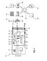
- FIG. 1 shows a schematic representation of the copy protection according to the invention for printed circuit boards. Shown is in a highly schematic simplification, a circuit board 10 with various active components 12, whose internal wiring in FIG. 1 not shown.
- the circuit board 10 has a plurality of terminals 14, where it is contacted in the installed position of corresponding contacts of an electronic device. Three of the ports, namely IN, OUT and COM, are particularly highlighted in FIG.
- the terminal IN forms with the terminal COM a pair of input terminals for a test signal 16, which is applied by a control unit not shown during normal operation of the electronic device, also not shown, in which the circuit board 10 is installed at a predetermined time ,
- the test signal 16 is a pulse signal.
- a network 18 comprising various passive electrical components.
- passive electrical components Purely by way of example are in FIG. 1 three inductors 20, four capacitors 22 and two ohmic resistors 24 shown.
- the exact number of passive electrical components and their concrete values, ie capacitance value, inductance value or ohmic resistance value, as well as the specific arrangement on the board relative to each other are not relevant to the present invention. Rather, the strength of the present invention lies in the almost unlimited variability of the design options that allow for a specific or even individual-board coding by the network of passive electrical components.
- the terminals OUT and COM together form a pair of output terminals at which a response signal 26 of the network 18 can be tapped.
- the response signal 26 is dependent on the input signal 16 and the characteristic of the network 18.
- FIGS FIG. 1 a schematic spectrum 16 'of the input signal 16 and a spectrum 26' of the output signal 26 are shown. The illustration is for the purpose of illustrating only that through the network 18, a signal applied to the input terminal pair IN / COM undergoes a characteristic change resulting in the output signal 26 being tapped at the output terminal pair OUT / COM.
- the control unit performs an analysis of the output signal 26, which may include spectral analysis, for example.
- the result of the analysis is compared with an expected value, which in the exemplary embodiment shown is stored as spectrum 36 'in a memory 28 of the control unit (decision block 30).
- the operation of the electronic device continues normally (result block 32). If the signal analysis result 26 'differs substantially from the expected value 36', the continued operation of the electronic device is at least partially prevented (event block 34).
- the components of the network 18 are not in the obvious manner, as in FIG. 1 shown schematically, applied to the board 10. Rather, the components are hidden.
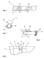
- FIG. 2 shows an example of the hidden arrangement of a capacitor 22, consisting of two conductor surfaces 221, 222, which are embedded in the acting as a dielectric plastic of the printed circuit board 10.
- Such not belonging to the network 18 conductor surfaces 221, 222 arise in many cases by "flooding" unnecessary circuit board surface and thus without additional costs in the usual board production.
- FIG. 3 shows an illustrative example of an inductor 20 as part of the network 18.
- the inductor 20 consists of a conductor 201 which is wound in a coil shape around an opening 202 of the board.
- the opening 202 serves to pass through a fastening bolt 203, with which the circuit board 10 is installed in the electronic device.
- the fastening bolt 203 is preferably made of a ferromagnetic material, so that its presence or absence as a coil core makes a significant difference in the inductance value of the inductor 20.
- FIG. 4 shows an illustrative example of a capacitance 22 of the network 18.
- the capacitance 22 consists of the conductor surfaces 221, 222 ".
- a first conductor surface 221 is part of the circuit board 10.
- the second conductor surface 222 is part of the electronic device into which the circuit board 10 is installed.
- An electrical connection of the device-side conductor surface 222 "to the rest of the network 18 via a guided in the electronic device connecting wire 223 which is connected to an electrically conductive fastening bolt 224, in turn, the rest of the network 18 via an electrically conductive aperture 225 of the Circuit board breakthrough 225 is electrically connected to the remainder of network 18.
- capacitance 22 only acts as a capacitance in the installation position of circuit board 10. In the insulated circuit board, it only provides a region of high ohmic resistance Resistance.
- FIG. 5 shows a variant of the network 18 which consists of two subnetworks 18 'and 18 ".
- the subnetworks 18', 18" are connected by means of a clamping contact 181 of the electronic device into which the circuit board 10 is installed by the clamping contact 181 two contact surface 182 'and 182 ", which are in each case components of the subnetworks 18', 18", electrically conductively contacted.
- the network 18 in installation position shows a completely different impulse response or transfer function than in the isolated state.
Landscapes
- Engineering & Computer Science (AREA)
- Computer Hardware Design (AREA)
- Microelectronics & Electronic Packaging (AREA)
- General Engineering & Computer Science (AREA)
- Physics & Mathematics (AREA)
- General Physics & Mathematics (AREA)
- Computer Security & Cryptography (AREA)
- Theoretical Computer Science (AREA)
- Software Systems (AREA)
- Tests Of Electronic Circuits (AREA)
Claims (2)
- Un dispositif électronique composé de ce qui suit :- une carte de circuits imprimés (10) comprenant un ensemble de contacts d'entrée (IN/COM), un ensemble de contacts de sortie (OUT/COM) et un circuit électrique (18) connecté entre les contacts d'entrée (IN/COM) d'une part et les contacts de sortie (OUT/COM) d'autre part ainsi que- un ou plusieurs composants de dispositifs ou composants d'installation (181) et- un contrôleur pour détecter une carte de circuits imprimés autre que celle d'origineoù le contrôleur est configuré pour, au moins une fois pendant l'exécution prévue du dispositif,- appliquer un signal de test prédéterminé (16) sous la forme d'un signal d'impulsion, d'un signal de courant alternatif dont la fréquence est prédéterminée ou d'un signal de courant alternatif (16) avec une séquence de fréquences prédéterminées, vers l'ensemble de contacts d'entrée (IN/COM),- capter un signal de réponse (26) au niveau de l'ensemble de contacts de sorties (OUT/COM),- effectuer une analyse du signal de réponse (26)- comparer un résultat (26') de l'analyse de signal à une valeur attendue (36') stockée dans une mémoire (28) du contrôleur et- désactiver au moins partiellement, ou ne pas activer, d'autres opérations du dispositif si une non-concordance est déterminée entre le résultat de l'analyse du signal (26') et la valeur attendue (36'),où le circuit électrique (18) est configuré comme un réseau passif doté d'une fonction de transfert caractéristique et composé d'au moins deux circuits partiels distincts (18', 18' ') qui, lorsqu'installés en circuits partiels distincts, sont connectés pour conduire électriquement par interaction avec un ou plusieurs composants de dispositifs et/ou composants d'installation (181), et le résultat d'analyse de signal est influencé par la connexion conductrice au moyen de la fonction de transfert du réseau passif.
- Une méthode de détection d'une carte de circuits imprimés autre que celle d'origine (10) qui possède un ensemble de contacts d'entrée (IN/COM), un ensemble de contacts de sortie (OUT/COM) et un circuit électrique (19) connecté entre les contacts d'entrée (IN/COM) d'une part et les contacts de sortie (OUT/COM) d'autre part, et comprenant les étapes suivantes :a) application d'un signal de test prédéterminé (16) sous la forme d'un signal d'impulsion, d'un signal de courant alternatif dont la fréquence est prédéterminée ou d'un signal de courant alternatif avec séquence de fréquences prédéterminées, à l'ensemble de contacts d'entrée (IN/COM),b) captage d'un signal de réponse (26) au niveau de l'ensemble de contacts de sorties (OUT/COM),c) exécution d'une analyse du signal de réponse (26),où un contrôleur est fourni pour- exécuter les étapes a à c au moins une fois pendant l'opération prévue d'un dispositif électronique dont les composants incluent un ou plusieurs composants de dispositif et/ou de composants d'installation (181), le contrôleur et la carte de circuits imprimés (10),- comparer un résultat (26') de l'analyse de signal à une valeur attendue (36') stockée dans une mémoire (28) du contrôleur et- désactiver au moins partiellement, ou ne pas activer, d'autres opérations du dispositif électronique si une non-concordance est déterminée entre le résultat de l'analyse du signal (26') et la valeur attendue (36'),où le circuit électrique (18) est configuré comme un réseau passif doté d'une fonction de transfert caractéristique et composé d'au moins deux circuits partiels distincts (18', 18' ') qui, lorsqu'installés en circuits partiels distincts, sont connectés pour conduire électriquement par interaction avec un ou plusieurs composants de dispositifs et/ou composants d'installation, et le résultat d'analyse de signal est influencé par la connexion conductrice via la fonction de transfert du réseau passif.
Applications Claiming Priority (2)
| Application Number | Priority Date | Filing Date | Title |
|---|---|---|---|
| DE102008026276A DE102008026276B4 (de) | 2008-06-02 | 2008-06-02 | Verfahren zum Untersuchen einer Leiterplatte und elektronisches Gerät |
| PCT/EP2009/003787 WO2009146830A1 (fr) | 2008-06-02 | 2009-05-28 | Appareil électronique et procédé de contrôle d'une carte de circuits imprimés |
Publications (2)
| Publication Number | Publication Date |
|---|---|
| EP2283718A1 EP2283718A1 (fr) | 2011-02-16 |
| EP2283718B1 true EP2283718B1 (fr) | 2012-03-28 |
Family
ID=40947584
Family Applications (3)
| Application Number | Title | Priority Date | Filing Date |
|---|---|---|---|
| EP09757211A Not-in-force EP2283716B1 (fr) | 2008-06-02 | 2009-05-28 | Appareil électronique et procédé de contrôle d'une carte de circuits imprimés |
| EP09757213A Not-in-force EP2283718B1 (fr) | 2008-06-02 | 2009-05-28 | Appareil électronique et procédé de contrôle d'une carte de circuits imprimés |
| EP09757212A Not-in-force EP2283717B1 (fr) | 2008-06-02 | 2009-05-28 | Appareil électronique et procédé de contrôle d'une carte de circuits imprimés |
Family Applications Before (1)
| Application Number | Title | Priority Date | Filing Date |
|---|---|---|---|
| EP09757211A Not-in-force EP2283716B1 (fr) | 2008-06-02 | 2009-05-28 | Appareil électronique et procédé de contrôle d'une carte de circuits imprimés |
Family Applications After (1)
| Application Number | Title | Priority Date | Filing Date |
|---|---|---|---|
| EP09757212A Not-in-force EP2283717B1 (fr) | 2008-06-02 | 2009-05-28 | Appareil électronique et procédé de contrôle d'une carte de circuits imprimés |
Country Status (6)
| Country | Link |
|---|---|
| US (3) | US8508236B2 (fr) |
| EP (3) | EP2283716B1 (fr) |
| CN (3) | CN102047769B (fr) |
| AT (3) | ATE551885T1 (fr) |
| DE (1) | DE102008026276B4 (fr) |
| WO (3) | WO2009146829A1 (fr) |
Families Citing this family (8)
| Publication number | Priority date | Publication date | Assignee | Title |
|---|---|---|---|---|
| DE102008026276B4 (de) * | 2008-06-02 | 2012-08-09 | Sartorius Weighing Technology Gmbh | Verfahren zum Untersuchen einer Leiterplatte und elektronisches Gerät |
| DE102010048036A1 (de) * | 2010-05-14 | 2012-08-30 | Häusermann GmbH | Leiterplatte mit Kopierschutz und Verfahren zur Herstellung und Anwendung |
| US9692476B2 (en) | 2012-04-25 | 2017-06-27 | 3M Innovative Properties Company | Wireless connectors |
| DE102012019645B4 (de) * | 2012-10-06 | 2025-01-09 | Volkswagen Aktiengesellschaft | Verfahren zum Testen einer Schaltung sowie entsprechende Schaltung |
| US9959430B2 (en) * | 2014-02-05 | 2018-05-01 | The United States Of America As Represented By The Secretary Of The Navy | Counterfeit microelectronics detection based on capacitive and inductive signatures |
| EP3478032B1 (fr) | 2017-10-24 | 2021-09-01 | VARTA Microbattery GmbH | Carte à circuit imprimé et utilisation d'un rail de protection d'arêtes |
| EP3861361B1 (fr) | 2018-10-01 | 2022-11-30 | Volkswagen Aktiengesellschaft | Procédé et dispositif servant à surveiller la fiabilité d'un système électronique |
| CN110287072A (zh) * | 2019-06-20 | 2019-09-27 | 深圳忆联信息系统有限公司 | 随机验证响应的方法、装置、计算机设备及存储介质 |
Family Cites Families (24)
| Publication number | Priority date | Publication date | Assignee | Title |
|---|---|---|---|---|
| US4675769A (en) * | 1985-11-15 | 1987-06-23 | Data General Corporation | Electronic board identification |
| DE3602960C1 (de) * | 1986-01-31 | 1987-02-19 | Philips Patentverwaltung | Dickschicht-Schaltungsanordnung mit einer keramischen Substratplatte |
| US4908576A (en) * | 1987-09-08 | 1990-03-13 | Jackson Daniel K | System for printed circuit board testing |
| US5203004A (en) * | 1990-01-08 | 1993-04-13 | Tandem Computers Incorporated | Multi-board system having electronic keying and preventing power to improperly connected plug-in board with improperly configured diode connections |
| JP2898814B2 (ja) * | 1992-02-25 | 1999-06-02 | 株式会社日立製作所 | 印刷インダクタ付き多層配線板 |
| DE4334355A1 (de) * | 1993-10-08 | 1995-04-13 | Vdo Schindling | Informationsgeber |
| US5588202A (en) * | 1995-03-17 | 1996-12-31 | Honeywell Inc. | Method for manufacturing an overmolded sensor |
| US5736862A (en) * | 1995-06-22 | 1998-04-07 | Genrad, Inc. | System for detecting faults in connections between integrated circuits and circuit board traces |
| JP3116863B2 (ja) | 1997-07-07 | 2000-12-11 | 日本電気株式会社 | デバイスシミュレーション方法 |
| MXPA02000550A (es) * | 1999-07-15 | 2002-07-02 | Thomson Licensing Sa | Metodo y aparato para dar soporte a dos diferentes tipos de tarjetas de circuito integrado con un unico conector. |
| JP2002366505A (ja) * | 2001-06-07 | 2002-12-20 | Nec Corp | 実装位置検出方法及び装置 |
| JP4318417B2 (ja) * | 2001-10-05 | 2009-08-26 | ソニー株式会社 | 高周波モジュール基板装置 |
| US7587695B2 (en) * | 2001-12-10 | 2009-09-08 | Mentor Graphics Corporation | Protection boundaries in a parallel printed circuit board design environment |
| US6606252B1 (en) * | 2002-07-17 | 2003-08-12 | Delphi Technologies, Inc. | Fastener detection for encased electrical assembly |
| US7230316B2 (en) * | 2002-12-27 | 2007-06-12 | Semiconductor Energy Laboratory Co., Ltd. | Semiconductor device having transferred integrated circuit |
| JP2005156212A (ja) * | 2003-11-21 | 2005-06-16 | Fuji Xerox Co Ltd | 回路基板検査装置 |
| TWM250504U (en) * | 2003-11-27 | 2004-11-11 | Optimum Care Int Tech Inc | Assembly structure for hiding electronic component |
| JP4362386B2 (ja) * | 2004-02-06 | 2009-11-11 | ソニー株式会社 | 電子回路基板、パネル型表示装置および製品の判別方法 |
| EP1607899B1 (fr) * | 2004-06-15 | 2007-08-15 | STMicroelectronics Limited | Détection de carte |
| US7772974B2 (en) * | 2005-02-28 | 2010-08-10 | Cypak Ab | Tamper evident seal system and method |
| DE112006003065T5 (de) * | 2005-10-28 | 2008-09-25 | Advantest Corporation | Prüfvorrichtung, Befestigungsplatte und Stiftelektronikkarte |
| DE102005062800A1 (de) | 2005-12-28 | 2007-07-12 | El-Me Ag | Elektronik-Sicherheits-Modul |
| JP2008026217A (ja) * | 2006-07-24 | 2008-02-07 | Toshiba Corp | 接近センサ及び電子機器 |
| DE102008026276B4 (de) * | 2008-06-02 | 2012-08-09 | Sartorius Weighing Technology Gmbh | Verfahren zum Untersuchen einer Leiterplatte und elektronisches Gerät |
-
2008
- 2008-06-02 DE DE102008026276A patent/DE102008026276B4/de not_active Expired - Fee Related
-
2009
- 2009-05-28 CN CN200980119796.XA patent/CN102047769B/zh not_active Expired - Fee Related
- 2009-05-28 CN CN200980119797.4A patent/CN102047770B/zh not_active Expired - Fee Related
- 2009-05-28 CN CN200980119800.2A patent/CN102047771B/zh not_active Expired - Fee Related
- 2009-05-28 AT AT09757213T patent/ATE551885T1/de active
- 2009-05-28 WO PCT/EP2009/003786 patent/WO2009146829A1/fr not_active Ceased
- 2009-05-28 EP EP09757211A patent/EP2283716B1/fr not_active Not-in-force
- 2009-05-28 WO PCT/EP2009/003785 patent/WO2009146828A1/fr not_active Ceased
- 2009-05-28 AT AT09757211T patent/ATE551883T1/de active
- 2009-05-28 EP EP09757213A patent/EP2283718B1/fr not_active Not-in-force
- 2009-05-28 AT AT09757212T patent/ATE551884T1/de active
- 2009-05-28 WO PCT/EP2009/003787 patent/WO2009146830A1/fr not_active Ceased
- 2009-05-28 EP EP09757212A patent/EP2283717B1/fr not_active Not-in-force
-
2010
- 2010-12-02 US US12/959,049 patent/US8508236B2/en not_active Expired - Fee Related
- 2010-12-02 US US12/958,869 patent/US8395407B2/en not_active Expired - Fee Related
- 2010-12-02 US US12/958,982 patent/US8508235B2/en not_active Expired - Fee Related
Also Published As
| Publication number | Publication date |
|---|---|
| CN102047771B (zh) | 2012-11-28 |
| ATE551884T1 (de) | 2012-04-15 |
| WO2009146829A1 (fr) | 2009-12-10 |
| DE102008026276A1 (de) | 2009-12-24 |
| EP2283717A1 (fr) | 2011-02-16 |
| US8508235B2 (en) | 2013-08-13 |
| WO2009146828A1 (fr) | 2009-12-10 |
| CN102047770A (zh) | 2011-05-04 |
| EP2283717B1 (fr) | 2012-03-28 |
| ATE551883T1 (de) | 2012-04-15 |
| CN102047769A (zh) | 2011-05-04 |
| US8395407B2 (en) | 2013-03-12 |
| DE102008026276B4 (de) | 2012-08-09 |
| EP2283716A1 (fr) | 2011-02-16 |
| EP2283718A1 (fr) | 2011-02-16 |
| CN102047770B (zh) | 2012-11-28 |
| US20110133752A1 (en) | 2011-06-09 |
| US20110133753A1 (en) | 2011-06-09 |
| US8508236B2 (en) | 2013-08-13 |
| EP2283716B1 (fr) | 2012-03-28 |
| CN102047769B (zh) | 2012-11-28 |
| ATE551885T1 (de) | 2012-04-15 |
| WO2009146830A1 (fr) | 2009-12-10 |
| CN102047771A (zh) | 2011-05-04 |
| US20110140731A1 (en) | 2011-06-16 |
Similar Documents
| Publication | Publication Date | Title |
|---|---|---|
| EP2283717B1 (fr) | Appareil électronique et procédé de contrôle d'une carte de circuits imprimés | |
| WO2000045332A1 (fr) | Carte a puce sans contact | |
| DE102016116695B4 (de) | Verfahren und Messvorrichtung zum Überprüfen eines Kabelbaumes | |
| WO2012084394A1 (fr) | Appareil de terrain comprenant une unité de batterie | |
| DE102010040558A1 (de) | Steuergerät und Verfahren zum Entwerfen einer Leiterplatte eines Steuergeräts | |
| DE102013223706A1 (de) | Überwachen von Steckverbindungszuständen | |
| DE102007022210B3 (de) | Mehrstufiges Verbindersystem für medizinische Verwendung | |
| EP3422027B1 (fr) | Dispositif, procédé, procédé de fabrication pour tester faisceaux de câbles | |
| EP2387798B1 (fr) | Procédé de vérification d'un circuit d'identification | |
| DE69223073T2 (de) | Datensicherheitsvorrichtung | |
| DE102008003986B3 (de) | Mainboard, elektronisches Gerät sowie Anordnung eines elektronischen Gerätes mit einer Spannungsversorgungseinheit | |
| EP1720122B1 (fr) | Procédé destiné à la création d'un support de données portatif | |
| DE69727105T2 (de) | Gerät für automatische Verbindungserkennung | |
| EP0920659B1 (fr) | Circuit a semi-conducteur protege contre les interventions exterieures | |
| EP2195760B1 (fr) | Dispositif de protection et procédé de fabrication d'un dispositif de protection | |
| EP1194857A1 (fr) | Procede pour marquer une variante materielle d'une unite materielle electrique ou electronique | |
| DE4115432A1 (de) | Schaltung zur stoerungserfassung fuer eine prozessorgesteuerte elektronische baugruppe | |
| DE19744925B4 (de) | Verfahren zum Erkennen unerwünschter offener Verbindungen | |
| EP3478032B1 (fr) | Carte à circuit imprimé et utilisation d'un rail de protection d'arêtes | |
| DE102023109399A1 (de) | Anordung von anreihbaren elektrischen Geräten | |
| DE102019131813A1 (de) | Verfahren zum Herstellen einer eine elektrische Schaltung umfassenden Leiterplatte für ein elektronisches Bremssystem für ein Fahrzeug | |
| EP0678820A2 (fr) | Lecteur de carte à chip à détection de manipulation frauduleuse |
Legal Events
| Date | Code | Title | Description |
|---|---|---|---|
| PUAI | Public reference made under article 153(3) epc to a published international application that has entered the european phase |
Free format text: ORIGINAL CODE: 0009012 |
|
| 17P | Request for examination filed |
Effective date: 20110103 |
|
| AK | Designated contracting states |
Kind code of ref document: A1 Designated state(s): AT BE BG CH CY CZ DE DK EE ES FI FR GB GR HR HU IE IS IT LI LT LU LV MC MK MT NL NO PL PT RO SE SI SK TR |
|
| AX | Request for extension of the european patent |
Extension state: AL BA RS |
|
| 17Q | First examination report despatched |
Effective date: 20110622 |
|
| RAP1 | Party data changed (applicant data changed or rights of an application transferred) |
Owner name: SARTORIUS WEIGHING TECHNOLOGY GMBH |
|
| DAX | Request for extension of the european patent (deleted) | ||
| GRAP | Despatch of communication of intention to grant a patent |
Free format text: ORIGINAL CODE: EPIDOSNIGR1 |
|
| RIC1 | Information provided on ipc code assigned before grant |
Ipc: H05K 1/02 20060101AFI20111125BHEP Ipc: G01R 31/3163 20060101ALI20111125BHEP |
|
| GRAS | Grant fee paid |
Free format text: ORIGINAL CODE: EPIDOSNIGR3 |
|
| GRAA | (expected) grant |
Free format text: ORIGINAL CODE: 0009210 |
|
| AK | Designated contracting states |
Kind code of ref document: B1 Designated state(s): AT BE BG CH CY CZ DE DK EE ES FI FR GB GR HR HU IE IS IT LI LT LU LV MC MK MT NL NO PL PT RO SE SI SK TR |
|
| REG | Reference to a national code |
Ref country code: GB Ref legal event code: FG4D Free format text: NOT ENGLISH |
|
| REG | Reference to a national code |
Ref country code: CH Ref legal event code: EP |
|
| REG | Reference to a national code |
Ref country code: AT Ref legal event code: REF Ref document number: 551885 Country of ref document: AT Kind code of ref document: T Effective date: 20120415 |
|
| REG | Reference to a national code |
Ref country code: IE Ref legal event code: FG4D Free format text: LANGUAGE OF EP DOCUMENT: GERMAN |
|
| REG | Reference to a national code |
Ref country code: DE Ref legal event code: R096 Ref document number: 502009003152 Country of ref document: DE Effective date: 20120524 |
|
| REG | Reference to a national code |
Ref country code: NL Ref legal event code: VDEP Effective date: 20120328 |
|
| PG25 | Lapsed in a contracting state [announced via postgrant information from national office to epo] |
Ref country code: LT Free format text: LAPSE BECAUSE OF FAILURE TO SUBMIT A TRANSLATION OF THE DESCRIPTION OR TO PAY THE FEE WITHIN THE PRESCRIBED TIME-LIMIT Effective date: 20120328 Ref country code: NO Free format text: LAPSE BECAUSE OF FAILURE TO SUBMIT A TRANSLATION OF THE DESCRIPTION OR TO PAY THE FEE WITHIN THE PRESCRIBED TIME-LIMIT Effective date: 20120628 Ref country code: HR Free format text: LAPSE BECAUSE OF FAILURE TO SUBMIT A TRANSLATION OF THE DESCRIPTION OR TO PAY THE FEE WITHIN THE PRESCRIBED TIME-LIMIT Effective date: 20120328 |
|
| LTIE | Lt: invalidation of european patent or patent extension |
Effective date: 20120328 |
|
| PG25 | Lapsed in a contracting state [announced via postgrant information from national office to epo] |
Ref country code: GR Free format text: LAPSE BECAUSE OF FAILURE TO SUBMIT A TRANSLATION OF THE DESCRIPTION OR TO PAY THE FEE WITHIN THE PRESCRIBED TIME-LIMIT Effective date: 20120629 Ref country code: FI Free format text: LAPSE BECAUSE OF FAILURE TO SUBMIT A TRANSLATION OF THE DESCRIPTION OR TO PAY THE FEE WITHIN THE PRESCRIBED TIME-LIMIT Effective date: 20120328 Ref country code: LV Free format text: LAPSE BECAUSE OF FAILURE TO SUBMIT A TRANSLATION OF THE DESCRIPTION OR TO PAY THE FEE WITHIN THE PRESCRIBED TIME-LIMIT Effective date: 20120328 |
|
| PG25 | Lapsed in a contracting state [announced via postgrant information from national office to epo] |
Ref country code: CY Free format text: LAPSE BECAUSE OF FAILURE TO SUBMIT A TRANSLATION OF THE DESCRIPTION OR TO PAY THE FEE WITHIN THE PRESCRIBED TIME-LIMIT Effective date: 20120328 |
|
| PG25 | Lapsed in a contracting state [announced via postgrant information from national office to epo] |
Ref country code: CZ Free format text: LAPSE BECAUSE OF FAILURE TO SUBMIT A TRANSLATION OF THE DESCRIPTION OR TO PAY THE FEE WITHIN THE PRESCRIBED TIME-LIMIT Effective date: 20120328 Ref country code: SE Free format text: LAPSE BECAUSE OF FAILURE TO SUBMIT A TRANSLATION OF THE DESCRIPTION OR TO PAY THE FEE WITHIN THE PRESCRIBED TIME-LIMIT Effective date: 20120328 Ref country code: EE Free format text: LAPSE BECAUSE OF FAILURE TO SUBMIT A TRANSLATION OF THE DESCRIPTION OR TO PAY THE FEE WITHIN THE PRESCRIBED TIME-LIMIT Effective date: 20120328 Ref country code: IS Free format text: LAPSE BECAUSE OF FAILURE TO SUBMIT A TRANSLATION OF THE DESCRIPTION OR TO PAY THE FEE WITHIN THE PRESCRIBED TIME-LIMIT Effective date: 20120728 Ref country code: SI Free format text: LAPSE BECAUSE OF FAILURE TO SUBMIT A TRANSLATION OF THE DESCRIPTION OR TO PAY THE FEE WITHIN THE PRESCRIBED TIME-LIMIT Effective date: 20120328 Ref country code: RO Free format text: LAPSE BECAUSE OF FAILURE TO SUBMIT A TRANSLATION OF THE DESCRIPTION OR TO PAY THE FEE WITHIN THE PRESCRIBED TIME-LIMIT Effective date: 20120328 Ref country code: PL Free format text: LAPSE BECAUSE OF FAILURE TO SUBMIT A TRANSLATION OF THE DESCRIPTION OR TO PAY THE FEE WITHIN THE PRESCRIBED TIME-LIMIT Effective date: 20120328 |
|
| BERE | Be: lapsed |
Owner name: SARTORIUS WEIGHING TECHNOLOGY G.M.B.H. Effective date: 20120531 |
|
| PG25 | Lapsed in a contracting state [announced via postgrant information from national office to epo] |
Ref country code: PT Free format text: LAPSE BECAUSE OF FAILURE TO SUBMIT A TRANSLATION OF THE DESCRIPTION OR TO PAY THE FEE WITHIN THE PRESCRIBED TIME-LIMIT Effective date: 20120730 Ref country code: SK Free format text: LAPSE BECAUSE OF FAILURE TO SUBMIT A TRANSLATION OF THE DESCRIPTION OR TO PAY THE FEE WITHIN THE PRESCRIBED TIME-LIMIT Effective date: 20120328 |
|
| PG25 | Lapsed in a contracting state [announced via postgrant information from national office to epo] |
Ref country code: MC Free format text: LAPSE BECAUSE OF NON-PAYMENT OF DUE FEES Effective date: 20120531 |
|
| PG25 | Lapsed in a contracting state [announced via postgrant information from national office to epo] |
Ref country code: DK Free format text: LAPSE BECAUSE OF FAILURE TO SUBMIT A TRANSLATION OF THE DESCRIPTION OR TO PAY THE FEE WITHIN THE PRESCRIBED TIME-LIMIT Effective date: 20120328 Ref country code: NL Free format text: LAPSE BECAUSE OF FAILURE TO SUBMIT A TRANSLATION OF THE DESCRIPTION OR TO PAY THE FEE WITHIN THE PRESCRIBED TIME-LIMIT Effective date: 20120328 |
|
| PLBE | No opposition filed within time limit |
Free format text: ORIGINAL CODE: 0009261 |
|
| STAA | Information on the status of an ep patent application or granted ep patent |
Free format text: STATUS: NO OPPOSITION FILED WITHIN TIME LIMIT |
|
| REG | Reference to a national code |
Ref country code: IE Ref legal event code: MM4A |
|
| PG25 | Lapsed in a contracting state [announced via postgrant information from national office to epo] |
Ref country code: IT Free format text: LAPSE BECAUSE OF FAILURE TO SUBMIT A TRANSLATION OF THE DESCRIPTION OR TO PAY THE FEE WITHIN THE PRESCRIBED TIME-LIMIT Effective date: 20120328 Ref country code: BE Free format text: LAPSE BECAUSE OF NON-PAYMENT OF DUE FEES Effective date: 20120531 Ref country code: MK Free format text: LAPSE BECAUSE OF FAILURE TO SUBMIT A TRANSLATION OF THE DESCRIPTION OR TO PAY THE FEE WITHIN THE PRESCRIBED TIME-LIMIT Effective date: 20120328 |
|
| 26N | No opposition filed |
Effective date: 20130103 |
|
| REG | Reference to a national code |
Ref country code: DE Ref legal event code: R097 Ref document number: 502009003152 Country of ref document: DE Effective date: 20130103 |
|
| PG25 | Lapsed in a contracting state [announced via postgrant information from national office to epo] |
Ref country code: ES Free format text: LAPSE BECAUSE OF FAILURE TO SUBMIT A TRANSLATION OF THE DESCRIPTION OR TO PAY THE FEE WITHIN THE PRESCRIBED TIME-LIMIT Effective date: 20120709 Ref country code: IE Free format text: LAPSE BECAUSE OF NON-PAYMENT OF DUE FEES Effective date: 20120528 |
|
| PG25 | Lapsed in a contracting state [announced via postgrant information from national office to epo] |
Ref country code: MT Free format text: LAPSE BECAUSE OF FAILURE TO SUBMIT A TRANSLATION OF THE DESCRIPTION OR TO PAY THE FEE WITHIN THE PRESCRIBED TIME-LIMIT Effective date: 20120328 Ref country code: BG Free format text: LAPSE BECAUSE OF FAILURE TO SUBMIT A TRANSLATION OF THE DESCRIPTION OR TO PAY THE FEE WITHIN THE PRESCRIBED TIME-LIMIT Effective date: 20120628 |
|
| REG | Reference to a national code |
Ref country code: DE Ref legal event code: R082 Ref document number: 502009003152 Country of ref document: DE Representative=s name: FIEDLER, OSTERMANN & SCHNEIDER, DE |
|
| REG | Reference to a national code |
Ref country code: DE Ref legal event code: R081 Ref document number: 502009003152 Country of ref document: DE Owner name: SARTORIUS LAB INSTRUMENTS GMBH & CO. KG, DE Free format text: FORMER OWNER: SARTORIUS WEIGHING TECHNOLOGY GMBH, 37075 GOETTINGEN, DE Effective date: 20130731 Ref country code: DE Ref legal event code: R082 Ref document number: 502009003152 Country of ref document: DE Representative=s name: FIEDLER, OSTERMANN & SCHNEIDER, DE Effective date: 20130731 |
|
| REG | Reference to a national code |
Ref country code: GB Ref legal event code: 732E Free format text: REGISTERED BETWEEN 20131024 AND 20131030 |
|
| REG | Reference to a national code |
Ref country code: FR Ref legal event code: TP Owner name: SARTORIUS LAB INSTRUMENTS GMBH & CO. KG, DE Effective date: 20131028 |
|
| REG | Reference to a national code |
Ref country code: CH Ref legal event code: PL |
|
| PG25 | Lapsed in a contracting state [announced via postgrant information from national office to epo] |
Ref country code: LI Free format text: LAPSE BECAUSE OF NON-PAYMENT OF DUE FEES Effective date: 20130531 Ref country code: CH Free format text: LAPSE BECAUSE OF NON-PAYMENT OF DUE FEES Effective date: 20130531 |
|
| PG25 | Lapsed in a contracting state [announced via postgrant information from national office to epo] |
Ref country code: TR Free format text: LAPSE BECAUSE OF FAILURE TO SUBMIT A TRANSLATION OF THE DESCRIPTION OR TO PAY THE FEE WITHIN THE PRESCRIBED TIME-LIMIT Effective date: 20120328 |
|
| PG25 | Lapsed in a contracting state [announced via postgrant information from national office to epo] |
Ref country code: LU Free format text: LAPSE BECAUSE OF NON-PAYMENT OF DUE FEES Effective date: 20120528 |
|
| PG25 | Lapsed in a contracting state [announced via postgrant information from national office to epo] |
Ref country code: HU Free format text: LAPSE BECAUSE OF FAILURE TO SUBMIT A TRANSLATION OF THE DESCRIPTION OR TO PAY THE FEE WITHIN THE PRESCRIBED TIME-LIMIT Effective date: 20090528 |
|
| REG | Reference to a national code |
Ref country code: FR Ref legal event code: PLFP Year of fee payment: 7 |
|
| REG | Reference to a national code |
Ref country code: AT Ref legal event code: MM01 Ref document number: 551885 Country of ref document: AT Kind code of ref document: T Effective date: 20140528 |
|
| PGFP | Annual fee paid to national office [announced via postgrant information from national office to epo] |
Ref country code: DE Payment date: 20150531 Year of fee payment: 7 Ref country code: GB Payment date: 20150527 Year of fee payment: 7 |
|
| PG25 | Lapsed in a contracting state [announced via postgrant information from national office to epo] |
Ref country code: AT Free format text: LAPSE BECAUSE OF NON-PAYMENT OF DUE FEES Effective date: 20140528 |
|
| PGFP | Annual fee paid to national office [announced via postgrant information from national office to epo] |
Ref country code: FR Payment date: 20150508 Year of fee payment: 7 |
|
| REG | Reference to a national code |
Ref country code: FR Ref legal event code: CA Effective date: 20160822 |
|
| REG | Reference to a national code |
Ref country code: DE Ref legal event code: R119 Ref document number: 502009003152 Country of ref document: DE |
|
| GBPC | Gb: european patent ceased through non-payment of renewal fee |
Effective date: 20160528 |
|
| REG | Reference to a national code |
Ref country code: FR Ref legal event code: ST Effective date: 20170131 |
|
| PG25 | Lapsed in a contracting state [announced via postgrant information from national office to epo] |
Ref country code: DE Free format text: LAPSE BECAUSE OF NON-PAYMENT OF DUE FEES Effective date: 20161201 Ref country code: FR Free format text: LAPSE BECAUSE OF NON-PAYMENT OF DUE FEES Effective date: 20160531 |
|
| PG25 | Lapsed in a contracting state [announced via postgrant information from national office to epo] |
Ref country code: GB Free format text: LAPSE BECAUSE OF NON-PAYMENT OF DUE FEES Effective date: 20160528 |