EP2284015A1 - Elément de sécurité et sa fabrication - Google Patents
Elément de sécurité et sa fabrication Download PDFInfo
- Publication number
- EP2284015A1 EP2284015A1 EP10014326A EP10014326A EP2284015A1 EP 2284015 A1 EP2284015 A1 EP 2284015A1 EP 10014326 A EP10014326 A EP 10014326A EP 10014326 A EP10014326 A EP 10014326A EP 2284015 A1 EP2284015 A1 EP 2284015A1
- Authority
- EP
- European Patent Office
- Prior art keywords
- security element
- subregions
- laser
- grid
- markings
- Prior art date
- Legal status (The legal status is an assumption and is not a legal conclusion. Google has not performed a legal analysis and makes no representation as to the accuracy of the status listed.)
- Granted
Links
- 238000004519 manufacturing process Methods 0.000 title abstract description 4
- 230000005855 radiation Effects 0.000 claims abstract description 75
- 238000000034 method Methods 0.000 claims abstract description 47
- 230000003287 optical effect Effects 0.000 claims abstract description 21
- 230000003993 interaction Effects 0.000 claims description 47
- 239000010409 thin film Substances 0.000 claims description 24
- 230000010287 polarization Effects 0.000 claims description 16
- 125000006850 spacer group Chemical group 0.000 claims description 16
- 230000009471 action Effects 0.000 claims description 15
- 239000010408 film Substances 0.000 claims description 13
- 239000006096 absorbing agent Substances 0.000 claims description 12
- 230000000694 effects Effects 0.000 claims description 12
- 230000008859 change Effects 0.000 claims description 11
- 238000004049 embossing Methods 0.000 claims description 4
- 239000011888 foil Substances 0.000 abstract description 4
- 238000012986 modification Methods 0.000 abstract 1
- 230000004048 modification Effects 0.000 abstract 1
- 229910052751 metal Inorganic materials 0.000 description 21
- 239000002184 metal Substances 0.000 description 21
- 238000010521 absorption reaction Methods 0.000 description 10
- 238000013461 design Methods 0.000 description 7
- 238000002372 labelling Methods 0.000 description 5
- 230000008569 process Effects 0.000 description 5
- 238000012876 topography Methods 0.000 description 5
- 206010013710 Drug interaction Diseases 0.000 description 4
- 230000001419 dependent effect Effects 0.000 description 4
- 238000001465 metallisation Methods 0.000 description 4
- 230000003595 spectral effect Effects 0.000 description 4
- 238000010330 laser marking Methods 0.000 description 3
- 229910052782 aluminium Inorganic materials 0.000 description 2
- XAGFODPZIPBFFR-UHFFFAOYSA-N aluminium Chemical compound [Al] XAGFODPZIPBFFR-UHFFFAOYSA-N 0.000 description 2
- 230000008901 benefit Effects 0.000 description 2
- 239000000969 carrier Substances 0.000 description 2
- 238000010276 construction Methods 0.000 description 2
- 238000001514 detection method Methods 0.000 description 2
- 210000003608 fece Anatomy 0.000 description 2
- 238000004806 packaging method and process Methods 0.000 description 2
- 239000000049 pigment Substances 0.000 description 2
- 229920003023 plastic Polymers 0.000 description 2
- 230000033458 reproduction Effects 0.000 description 2
- 239000000758 substrate Substances 0.000 description 2
- 238000007740 vapor deposition Methods 0.000 description 2
- 230000000007 visual effect Effects 0.000 description 2
- 238000005406 washing Methods 0.000 description 2
- VYZAMTAEIAYCRO-UHFFFAOYSA-N Chromium Chemical compound [Cr] VYZAMTAEIAYCRO-UHFFFAOYSA-N 0.000 description 1
- 229910004298 SiO 2 Inorganic materials 0.000 description 1
- 238000002679 ablation Methods 0.000 description 1
- 230000001133 acceleration Effects 0.000 description 1
- 229910052804 chromium Inorganic materials 0.000 description 1
- 239000011651 chromium Substances 0.000 description 1
- 238000007796 conventional method Methods 0.000 description 1
- 230000007547 defect Effects 0.000 description 1
- 238000011161 development Methods 0.000 description 1
- 230000018109 developmental process Effects 0.000 description 1
- 238000001035 drying Methods 0.000 description 1
- 238000010894 electron beam technology Methods 0.000 description 1
- 230000008030 elimination Effects 0.000 description 1
- 238000003379 elimination reaction Methods 0.000 description 1
- 238000005530 etching Methods 0.000 description 1
- 238000001704 evaporation Methods 0.000 description 1
- 238000003780 insertion Methods 0.000 description 1
- 230000037431 insertion Effects 0.000 description 1
- 238000011031 large-scale manufacturing process Methods 0.000 description 1
- 239000000463 material Substances 0.000 description 1
- 230000010355 oscillation Effects 0.000 description 1
- 239000003973 paint Substances 0.000 description 1
- 239000002904 solvent Substances 0.000 description 1
- 239000000126 substance Substances 0.000 description 1
- 238000012795 verification Methods 0.000 description 1
Images


Classifications
-
- B—PERFORMING OPERATIONS; TRANSPORTING
- B41—PRINTING; LINING MACHINES; TYPEWRITERS; STAMPS
- B41M—PRINTING, DUPLICATING, MARKING, OR COPYING PROCESSES; COLOUR PRINTING
- B41M3/00—Printing processes to produce particular kinds of printed work, e.g. patterns
- B41M3/14—Security printing
-
- B—PERFORMING OPERATIONS; TRANSPORTING
- B42—BOOKBINDING; ALBUMS; FILES; SPECIAL PRINTED MATTER
- B42D—BOOKS; BOOK COVERS; LOOSE LEAVES; PRINTED MATTER CHARACTERISED BY IDENTIFICATION OR SECURITY FEATURES; PRINTED MATTER OF SPECIAL FORMAT OR STYLE NOT OTHERWISE PROVIDED FOR; DEVICES FOR USE THEREWITH AND NOT OTHERWISE PROVIDED FOR; MOVABLE-STRIP WRITING OR READING APPARATUS
- B42D25/00—Information-bearing cards or sheet-like structures characterised by identification or security features; Manufacture thereof
- B42D25/30—Identification or security features, e.g. for preventing forgery
- B42D25/355—Security threads
-
- B—PERFORMING OPERATIONS; TRANSPORTING
- B41—PRINTING; LINING MACHINES; TYPEWRITERS; STAMPS
- B41M—PRINTING, DUPLICATING, MARKING, OR COPYING PROCESSES; COLOUR PRINTING
- B41M5/00—Duplicating or marking methods; Sheet materials for use therein
- B41M5/24—Ablative recording, e.g. by burning marks; Spark recording
-
- B—PERFORMING OPERATIONS; TRANSPORTING
- B41—PRINTING; LINING MACHINES; TYPEWRITERS; STAMPS
- B41M—PRINTING, DUPLICATING, MARKING, OR COPYING PROCESSES; COLOUR PRINTING
- B41M5/00—Duplicating or marking methods; Sheet materials for use therein
- B41M5/26—Thermography ; Marking by high energetic means, e.g. laser otherwise than by burning, and characterised by the material used
-
- G—PHYSICS
- G03—PHOTOGRAPHY; CINEMATOGRAPHY; ANALOGOUS TECHNIQUES USING WAVES OTHER THAN OPTICAL WAVES; ELECTROGRAPHY; HOLOGRAPHY
- G03H—HOLOGRAPHIC PROCESSES OR APPARATUS
- G03H1/00—Holographic processes or apparatus using light, infrared or ultraviolet waves for obtaining holograms or for obtaining an image from them; Details peculiar thereto
- G03H1/26—Processes or apparatus specially adapted to produce multiple sub- holograms or to obtain images from them, e.g. multicolour technique
- G03H1/30—Processes or apparatus specially adapted to produce multiple sub- holograms or to obtain images from them, e.g. multicolour technique discrete holograms only
- G03H2001/303—Interleaved sub-holograms, e.g. three RGB sub-holograms having interleaved pixels for reconstructing coloured holobject
Definitions
- the invention relates to a security element, in particular for a document of value, with a reflective layer, in which by the action of laser radiation visually recognizable markings in the form of patterns, letters, numbers or images are introduced.
- the invention further relates to a data carrier with such a security element and to methods and a device for producing such a security element.
- Data carriers such as valuables or identity documents, or other valuables, such as branded articles, are often provided with security elements for the purpose of security, which permit verification of the authenticity of the data carrier and at the same time serve as protection against unauthorized reproduction.
- Data carriers in the sense of the present invention are in particular bank notes, shares, bonds, certificates, vouchers, checks, high-quality admission tickets, but also other papers which are subject to counterfeiting, such as passports and other identity documents, as well as product security elements such as labels, seals, packaging and the like.
- the term "data carrier” in the following includes all such objects, documents and product protection means.
- optically variable elements are therefore used as security elements, which convey the viewer a different image impression, for example a different color impression, at different viewing angles.
- security elements come with optical diffraction structures, such as holograms, holographic Grid images and other hologram-like diffraction structures are used, which reconstruct different images from different viewing angles. Such viewing angle dependent effects can not be reproduced with normal copying or printing techniques.
- partial transparency areas in metal layers such as the reflection layers of the mentioned holograms or hologram-like diffraction structures, are often added later in the security area.
- see-through areas are usually produced by etching or washing.
- the positional accuracy of the demetallization pattern is limited by the positional accuracy of the printing operation.
- the demetallization pattern can usually have a few tenths of a millimeter tolerance to any other motifs present on the carrier film, such as holographic motifs or other print motifs. For very small film areas with high subject density, this can be disadvantageous.
- the demetallization patterns are subject to variations in detail as they result from the printing process, which can be a problem for very small labels, such as microtext in security threads.
- the publication EP 1 197 350 A2 describes a specific embodiment of a diffraction-optical security element, namely an optical element for value documents, which has a two-channel hologram for the reconstruction of holographic images from different viewing directions.
- Each holographically reproduced image which can be visually recognized only in one line of sight, corresponds to a channel.
- the individual channels are each assigned different surface areas of the hologram.
- the region of the hologram corresponding to a channel may be divided into a plurality of subregions. These subregions are designed, for example, as narrow strips.
- the belonging to different channels strips are preferably arranged alternately.
- the respective associated subregions of a diffractive optical image are spaced apart from each other, they produce a common diffraction image at the predetermined defined viewing angle.
- subareas are preferably changed with the aid of a laser so that they no longer participate in the image reconstruction and represent information in front of the holographic background.
- the object of the invention is to provide a security element which avoids the disadvantages of the prior art.
- the desired markings should be able to enroll quickly and with reasonable equipment expense in the security element.
- the reflection layer of a security element of the aforementioned type has a first subregion with an interference structure and a second subregion, the two subregions interacting differently with the laser radiation, so that the markings are due to a change in the optical properties caused by the action of the laser radiation the reflective layer of at least one of the two subregions are visually recognizable.
- the different interaction of the subregions can be used, for example, to decouple the positional accuracy of the introduced markings from the positional accuracy of the laser inscription and thus to produce high-precision markings in spite of simple and fast beam guidance.
- the nested sub-areas having an extent below the resolution limit of the naked eye, the differences in the interaction can be exploited to selectively introduce a label in one of the sub-areas, without having to make a detection of each currently detected by the laser writer sub-area.
- the markings can be introduced only in the first subarea or in both subregions. In the latter case, two labeling steps are generally required, wherein in a first labeling step, a marking is introduced into the first subarea and, in a second inscription step, an identifier is introduced into the second subarea.
- a marking is introduced into the first subarea and, in a second inscription step, an identifier is introduced into the second subarea.
- the polarization of the laser radiation and / or the orientation of the security element to be labeled is suitably changed between the first and second inscription steps.
- the first subregion contains as an interference structure a relief structure in the form of a grid pattern which is defined by a first grid constant and a first orientation of the grid lines.
- the second subarea has no interference structure, so that the different interaction is essentially determined by the properties of the interference structure of the first subarea.
- the second subarea contains a relief structure in the form of a grid pattern, which is defined by a second grid constant and a second orientation of the grid lines.
- both subregions contain a grid pattern
- a different interaction can advantageously be achieved in that the second grid constant and / or the second orientation of the grid lines of the second subarea differs from the first grid constant or the first orientation of the grid lines of the first subarea.
- the second orientation of the grid lines may be substantially perpendicular to the first orientation to achieve a different interaction with linearly polarized radiation.
- the two partial regions have a grid pattern with a lattice constant of 200 to 2000 nm, preferably of 500 to 1000 nm, and with different orientation of the grid lines.
- Another possibility for producing a different interaction for two subregions filled with grid patterns consists in the use of grid patterns with different grid profiles for the first and second subarea.
- the grid pattern of the security element are formed by rectangular grid.
- the grid lines are electrically isolated from each other, preferably by metal-free areas on the flanks of the rectangular grid.
- variants of the invention in which the two subregions interact to different degrees with polarized laser radiation. This can easily achieve a significant difference in the strength of the interaction.
- the security elements contain as an interference structure a thin-film element with a color-shift effect.
- the thin-film element expediently has a reflection layer, an absorber layer and a dielectric spacer layer arranged between the reflection layer and the absorber layer.
- both partial regions contain thin-film elements with a color-shift effect, and that the thickness of the dielectric spacer layer of the thin-film elements is different in the two partial regions.
- the invention is based in this aspect on the idea that by selecting the thickness of the dielectric spacer layer and the strength of the interaction of the thin-film elements can be determined with laser radiation of a certain wavelength. If the thin-film elements in the two subregions are designed with significantly different absorption for the selected laser wavelength, the marking can be carried out as in the exemplary embodiments described above. If the marking is carried out in particular by means of an IR laser, the thin-film elements in the visible spectral range can have identical or different color-shift effects, depending on the desired design.
- the two subregions are formed from subregions nested in each other. If both partial areas are provided with markings, they can also be nested inside each other.
- the subregions can in particular consist of parallel strips, preferably with a strip width between 10 .mu.m and 500 .mu.m.
- the first subregion contains a surface-enlarging relief structure, preferably a surface-enlarging relief structure with a crossed sinusoidal surface topography.
- the surface topography may, for example, a height of 50 to 5000 nm, preferably from 100 to 500 nm, and in the x and y direction each have a lattice constant of 200 to 1000 nm.
- the second subarea advantageously has no relief structure. Is exploited in this design that the surface of the security element increased by deliberately introducing a surface relief in this sub-area and the thickness of a metal layer deposited thereon can thus be reduced. The thinner metal layer can be removed in the demetalization step with a laser power that does not yet remove the thicker metal layer, so that there are also different interactions with the laser radiation here.
- the reflection layer is part of one or more optically variable structures, in particular a hologram, a holographic grating image or another hologram-like diffraction structure.
- the register fluctuations between the visually recognizable markings and the one or more optically variable structures are advantageously less than 10 .mu.m, in particular less than 5 .mu.m.
- the first subarea of the security element is advantageously produced as a relief structure with a grid pattern that is defined by a first grid constant and a first orientation of the grid lines.
- the second subarea of the security element can also be suitably generated as a relief structure with a grid pattern that is defined by a second grid constant and a second orientation of the grid lines.
- the security element is preferably exposed to laser radiation whose wavelength is greater than the first and / or the second lattice constant.
- the dependence of the interaction on the polarization of the laser radiation is utilized, in another the dependence of the interaction on the lattice constant in the two partial areas.
- Another variant uses the dependence of the interaction on the orientation of the grid lines in the two subregions. The dependence of the interaction of the grid profile in the two sub-areas can be exploited.
- the security element for marking is subjected to linearly polarized laser radiation, the polarization vector of which is selected essentially parallel to the grid lines of the subarea into which the marking is to be introduced.
- the laser power in the case of continuous wave lasers
- the laser energy in the case of pulsed lasers
- the laser power is suitably set so that its intensity is sufficient to remove the reflection layer in the first subregion due to the different interaction strength, whereas in the second subregion it does not yet suffice to remove the Reflection layer is sufficient.
- the security element for identification with radiation of an infrared laser in the wavelength range from 0.8 ⁇ m to 3 ⁇ m, in particular a Nd: YAG laser.
- the solution according to the invention allows the use of an expanded laser beam which at least partially detects both partial regions at the same time.
- the security element can be moved for identification under an expanded laser beam, wherein the expanded laser beam detects the entire region of the security element to be marked perpendicular to the direction of movement. On a deflection of the laser beam can be completely dispensed with.
- the security element for identification under a laser beam is moved through and deflected the laser beam perpendicular to the direction of movement of the security element.
- the laser beam can, but does not necessarily have to be widened.
- the invention also includes an apparatus for carrying out the described method with means for producing a security element having a first subarea with a relief structure and with a second subarea, means for applying a reflection layer to the first and second subarea, and a laser source for introducing the identifications, which are visually recognizable due to a change in the optical properties of the reflection layer of at least one of the two subregions caused by the action of the laser radiation.
- the laser source is preferably an infrared laser in the wavelength range from 0.8 ⁇ m to 3 ⁇ m, in particular a Nd: YAG laser at 1.06 ⁇ m.
- the apparatus may further include a polarizer for adjustably polarizing the laser radiation, optical elements for expanding the laser beam to a desired size of the laser spot, a deflector for directing the laser beam, and / or a transport device for guiding security elements disposed on a web.
- the invention further comprises a data carrier, in particular a value document, such as a banknote, an identity card or the like, which is provided with a security element of the type described.
- a data carrier in particular a value document, such as a banknote, an identity card or the like, which is provided with a security element of the type described.
- a continuous film equipped with a security element of the type described, in particular an embossing film, is also part of the invention.
- a particular advantage of the invention is seen in the possibility of introducing negative markings, such as negative text, precisely in hologram foils. While with conventional demetallization methods, registering the demetallized areas in a given hologram design is often difficult and results in undesirable variations in the positioning of the demetallized areas can, the invention allows for the first time, a zero tolerance between
- Fig. 1 shows a banknote 10, which is provided with at least one security element 12 according to the invention.
- the banknote may also have other security elements, such as a security thread 14.
- the security thread 14 is shown as a window security thread.
- Such a window security thread is only partially embedded in the banknote paper and occurs in certain areas 16, which are hatched in the figure, directly to the surface of the banknote 10.
- the security element 12 according to the invention is shown in the embodiment as a rectangular label, are introduced into the by the action of laser radiation visually recognizable markings 18 in the form of patterns, letters, numbers or images. It is understood that the security element 12 can also have any other shape.
- the security element 12 may be arranged on the banknote surface in the form of a broad strip which extends over the entire length or width of the banknote.
- the security element 12 can also be executed in the form of a security thread and like the illustrated security thread 14 embedded as a window security thread in the banknote 10.
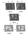
- Fig. 2 schematically a section of a security element 20, such as the rectangular label 12 of Fig.1.
- Fig. 2 (a) shows the security element 20 thereby, Fig. 2 (b) after exposure to laser radiation.
- laser sources all customary in personalization laser recorders can be used.
- a Nd: YAG-based laser writer with a wavelength of 1.064 ⁇ m is selected as the laser source, the radiation of which is linearly polarized before being acted upon by a polarization filter placed in the beam path.
- the security element 20 includes a metallic reflective layer 22 having a first portion 24 and a second portion 26 that differ in the strength of their interaction with the radiation of the selected Nd: YAG laser.
- the interaction properties of the subregions are tuned to the laser radiation in the manner described below in such a way that subregion 24 interacts significantly more strongly with laser radiation than subregion 26.
- the shape of subregion 24 within the surrounding subregion 26 provides the desired identification, in the exemplary embodiment the letter sequence "PL", dar.
- the energy or power of the laser source is now adjusted so that it is sufficient in the more strongly interacting subregion 24 for demetallization of the reflection layer 22, while it does not yet cause any demetallization in the weakly interacting subregion 26. It is therefore not necessary, in contrast to conventional labeling method, to follow the laser spot exactly the shape of the label to be introduced. Rather, it is sufficient if the laser radiation passes over the partial area 24 in order to demetallize the partial area 24 completely and with exact outline guidance, as in FIG Fig. 2 (b) shown.
- the accuracy of the laser deflection no longer determines the accuracy of the introduced marking can be deflected much faster around corners and the total demetallization over conventional laser demetallization can be significantly accelerated.
- the substrate to be processed can be scanned line by line at a high feed rate.
- a very strong laser with a wide-spread beam can be used, the no longer has to be distracted, but in which only the moving web with the demetall areden security elements under the light spot must be moved through.
- the shape of the demetallized areas is then determined solely by the shape of the more strongly interacting portion 24. Overall, there is a significant acceleration, simplification and increased precision of the laser marking.
- the different interaction strengths of the partial regions 24 and 26 with the radiation of the selected laser source can be achieved in various ways, as shown in detail below.
- At least one of the partial regions contains a relief structure, in particular a lattice pattern, which is defined by a lattice constant, an orientation of the lattice lines and a lattice profile.
- a lattice pattern which is defined by a lattice constant, an orientation of the lattice lines and a lattice profile.
- Such grid patterns can be produced very precisely with known originating and embossing techniques with arbitrary grid parameters.
- the grid pattern not only serve in the present description in the foreground standing simple and quick identification, but contribute by their diffraction properties in a conventional manner to increase the security against counterfeiting provided with the security elements.
- the interaction of the metallized diffraction gratings with the laser radiation depends strongly on the relative size of lattice constant and wavelength, and on polarized laser radiation also on the relative orientation of the grid lines and the direction of polarization of the radiation.
- the absorption properties of gratings with a lattice constant which is smaller than the laser wavelength used are strongly polarization-dependent.
- this strong polarization dependence in metallized lattice structures is explained by the fact that the laser radiation strongly excites the electron gas of the metal in a parallel to the electrically conductive grid lines polarization vector, so that a strong interaction of the incident light with the metal layer takes place. A large proportion of the radiation is reflected and a certain proportion is absorbed. On the other hand, if the polarization vector is inclined or even perpendicular to the orientation of the grating lines, then it finds a significantly lower conductivity in the direction of oscillation. The electron gas can hardly be excited to vibrate and it results in a much smaller interaction strength. The incident radiation is transmitted to a large extent. Only a small proportion is reflected and absorbed.
- FIG. 3 illustrates in (a) to (d) various possibilities of achieving a different interaction strength for two partial regions 32 and 34 by means of differently formed lattice patterns.
- the FIGS. 3 (c) and (d) show a security element 20 in such a boundary region in cross section.
- the sub-areas 32 and 34 are each filled with a grid pattern with a lattice constant of 900 nm, wherein the grid lines are perpendicular to each other in the two sub-areas.
- the security element 20 with suitably oriented, linearly polarized radiation of an Nd: YAG laser, it is possible to achieve that only the strongly interacting subregion is demetallized, but the weakly interacting subregion remains unaffected.
- Fig. 3 (b) As shown alternatively or additionally, the dependence of the interaction strength on the lattice constant of the lattice patterns in the subregions 32 and 34 can be exploited.
- the grating profile also influences the strength of the interaction with the laser radiation, so that a different absorption can also be achieved by differently blazed gratings in the two subregions 32 and 34, as in FIG Fig. 3 (c) shown. Also grid patterns with rounded grid profiles are suitable for this, as in Fig. 3 (d) illustrated.
- FIG. 4 (a) shows an idealized cross section through such a structure 100 with a rectangular profile 102 and an applied metallic reflection layer 104. It is understood that the rectangular grid 102 shown in the figure and the metallization 104 are slightly rounded in real structures. A particularly pronounced anisotropy of the absorption can be achieved if the individual grid lines of the rectangular grid 102 are electrically insulated from one another by missing metallization on their flanks 106, as in FIG Fig. 4 (a) shown.
- FIGS. 4 (b) and (c) show an embodiment in which two partial regions 112 and 114 abut with each other by 90 ° to each other rotated orientation of the respective rectangular lattice structures.
- Fig. 4 (b) shows a plan view of a small section 110 in the border region of the two subregions 112, 114 and
- Fig. 4 (c) shows a cross section along the line CC of Fig. 4 (b) ,
- the metallization 104 is in FIG Fig. 4 (c) not shown.
- the various subregions have an expansion which can be resolved with the naked eye.
- the information to be introduced can be given in particular by the shape of the subregions themselves, such as in Fig. 2 illustrated.
- the different absorption behavior of the subregions is exploited in order to decouple the positional accuracy of the introduced markings from the positional accuracy of the laser beam guidance and thus to produce high-precision markings in spite of simple and fast beam guidance.
- the subregions consist of nested subregions with an extent below the resolution limit of the naked eye.
- the subregions assigned to the various partial areas are in this case filled with grid patterns which reconstruct diffraction-optical images in different viewing directions.
- the different absorption behavior of the subregions is exploited in order to introduce a marking specifically into one of the subareas with a laser recorder without having to perform a recognition of the subarea currently being detected by the inscribing laser beam.
- the security element 40 has, as the first subregion, a first hologram region 42, which reconstructs a first diffraction-optical image when viewed obliquely from the left (arrow L). As a second subregion, the security element 40 has a second hologram region 44, which reconstructs a second diffraction-optical image when viewed obliquely from the right (arrow R).
- the hologram regions 42, 44 are divided into strip-shaped subregions 42-1 to 42-5 and 44-1 to 44-5, which each have a width of only 20 ⁇ m in the exemplary embodiment and thus can not be resolved with the naked eye.
- the subregions 42-1 to 42-5 and 44-1 to 44-5 of the two hologram regions 42, 44 are interleaved. In the exemplary embodiment shown, they are arranged alternately so that the subregion 42-1 of the first hologram region 42 is followed by the subregion 44-1 of the second hologram region 44, followed by the subregion 42-2 of the first hologram region, and so on.
- the individual sub-areas 42-1 to 42-5 and 44-1 to 44-5 are spaced apart from each other, the observer can see the holograms 42, 44 recognizable from the respective viewing directions (L and R, respectively) due to the small width and small spacing of the subregions contiguous. It is understood that the hologram regions 42, 44 may have any number of such subregions 42-1 to 42-n and 44-1 to 44-m, respectively. Also, the width of the subregions need not be identical.
- the production of the strip-shaped subregions can take place, for example, by means of a line mask, which, when an optical diffraction recording medium is exposed, covers the part of the recording medium which is not to be exposed. Alternatively, the strips may also be generated directly by appropriate control of an electron beam in a recording medium.
- the number of subregions or strips can also be chosen arbitrarily and, for example, 2500 with a strip width of 20 .mu.m.
- the two hologram regions 42, 44 (in FIG Fig. 5 not shown) markings in the form of sub-areas introduced that participate neither in the image reconstruction in the direction L nor in the direction R.
- the markings should be visible to the naked eye, so they usually extend over a large number of strips 42-i and 44-j. If the markings are to be introduced only in one of the hologram regions, or if the two hologram regions are to be provided with different markings, it must therefore be ensured that the stripes of each hologram region are provided only with the marking desired for this viewing direction.
- Fig. 6 (a) shows a section of the security element 40 before the laser marking.
- the narrow stripes are 42-i and 44-j, respectively for the reconstruction of the diffraction images in the viewing direction L or R filled with different lattice patterns.
- the polarization direction of the inscription laser is now selected so that a strong interaction with the grating patterns of the strips 42-i of the first hologram region 42 takes place and the interaction with the grating patterns of the strips 44-j of the second hologram region 44 is only weak.
- the subsequent inscription step then leads only in the strips 42-i, but not in the strips 44-j for demetallization of the reflection layer applied to the gratings.
- a first marking 52 here the letter sequence "PL"
- PL the letter sequence
- the polarization direction of the laser beam is adjusted to the orientation of the grating lines in the second hologram region 44, so that now a strong interaction with the lattice patterns of the strips 44-j of the second hologram region 44 takes place and the interaction with the lattice patterns of the strips 42-i of the first hologram region 42 is only weak.
- a second identifier 54 in this case the numerical sequence "12", written in the second hologram region 44, again without the laser beam to align the respective stripes since the inscription step results in demetallization of the reflection layer applied to the gratings only in the strips 44-j, but not in the likewise detected strips 42-i.
- Fig. 6 (c) The marked strip sequence shown in FIG. 1, in which the strips 42-i and 44-j are provided with different markings.
- the demetallized areas 52, 54 no longer contribute to the image reconstruction in the respective viewing direction of the holograms 42 and 44 and thus form defects in the reconstructed holograms.
- the information content of these areas 52, 54 thus emerges to the viewer from the respective viewing direction as a dark-appearing marking against the background of the bright diffraction images, as in FIG FIGS. 6 (d) and (e) shown.
- Fig. 7 shows in cross section a further embodiment of the invention, the structure of which initially largely the security element 40 of Fig. 6 equivalent.
- the security element 60 is the Fig. 7 executed in accordance with the security element 40 as Regehologramm. It therefore has two transparent plastic layers 62 and 64 whose boundary surface is in the form of embossed diffraction structures 66 and 68, respectively.
- the section of the Fig. 7 shows two strips each 42-1 and 42-2 and 44-1 and 44-2 of the two hologram regions 42 and 44.
- the types of stripes differ in their lattice pattern, so that the interface in the strips 42-1 and 42-2 with a first diffraction structure 66 while the interface of the strips 44-1 and 44-2 has a second diffraction structure 68.
- the entire boundary area between the plastic layers 62, 64 is provided with a reflective layer 70, which in the strips 42-1 and 42-2 recesses 72 and in the strips 44-1 and 44-2 recesses 74, whose shape just correspond to the above-described, produced by demetallization of the reflective layer markings 52 and 54, respectively.
- the reflection layer 70 is preferably a thin metal layer, for example an aluminum layer.
- the security element 40 is particularly suitable for securing translucent or transparent valuables, since the recesses 72, 74 can be seen as bright, strongly contrasting areas in front of the dark-appearing, remaining reflection layer 70 when viewed in transmitted light.
- the security element 60 below the reflective layer 70 of the holograms 42, 44 contains another metal layer 76 with the same visual appearance as the reflective layer 70. Looking at the security element 60 from a direction other than the excellent viewing directions L and R, then partially demetallized reflective layer 70 of the holograms and visible through the demetallinstrumenten areas 52, 54 visible further metal layer 76 together as a homogeneous and structureless, shiny metallic surface, so that the labels from these directions are not visible.
- the security elements 40, 60 can have further hologram regions, which are correspondingly nested with the hologram regions 42, 44.
- FIG. 8 Another embodiment of the invention is in Fig. 8 shown.
- the security element 80 shown there has two hologram areas 82 and 84, which are provided with diffraction patterns designed for different viewing angles, a third diffractive optical image area 88.
- the hologram regions 82, 84 and 88 are, as already at Fig. 5 are each divided into a plurality of narrow strips 82-i, 84-i and 88-i, which are arranged nested one inside the other.
- the hologram regions 82 and 84 also have the above-described markings, while the hologram region 88 is formed without markings and can be seen at a different viewing angle from the hologram regions 82 and 84, for example when the security element 80 is viewed vertically.
- the observer then recognizes, on oblique viewing from the left, the image reconstructed by the stripes 82-i with the first marking inscribed therein, and viewed obliquely from the right the image reconstructed by the stripes 84-i with the second marking inscribed therein and from the vertical viewing direction the image reconstructed from stripes 88-i without marking.
- the hologram area 88 can reconstruct a complex and aesthetically pleasing image, while the designated hologram areas 82 and 84 can be designed very simply and show, for example, only the marking in front of a monochrome background from the respective viewing direction.
- a differently strong interaction of the laser radiation is achieved with the security element in contrast to the previously described embodiments by the use of suitably designed thin-film interference elements with color shift effect.
- Such thin-film elements have a layer structure with a reflection layer, an absorber layer and between a reflection layer and absorber layer disposed dielectric spacer layer.
- the color shift effect is based on viewing angle-dependent interference effects due to multiple reflections in the different sub-layers of the thin-film element.
- the path difference of the light reflected at the different layers depends on the one hand on the optical thickness of the dielectric spacer layer and on the other hand varies with the respective viewing angle.
- the thickness of the dielectric spacer layer in addition to the appearance of the element in the visible spectral range and the strength of the absorption for laser radiation outside the visible range can be varied over a wide range.
- the marking can be carried out as in the exemplary embodiments described above. Since the marking preferably takes place with infrared lasers, the thin-film elements of the subregions can be designed as desired so that they realize identical or different color-shift effects in the visible spectral range.
- the labeling can also be done by laser recorders in the visible spectral range, but the variations for the visual appearance of the elements are then usually lower.
- Fig. 9 (a) shows analogous to the embodiment of Fig. 5 a plan view of a security element 120 with an alternating sequence of strip-shaped sub-areas 122, 124.
- the security element 120 has a substrate film 126, on which an aluminum reflection layer 128, an SiO 2 dielectric layer 130 and a semitransparent chromium absorber layer 132 are deposited.
- the thickness of the dielectric layer 130 is chosen differently in the subregions 122 and 124 in order to achieve a different absorption of the laser radiation used for the marking.
- the layer thicknesses that the absorption for this wavelength in the subregions 124 is 0.8 or even 0.9 exceeds while it is below 0.4 in the subregions 122.
- the sub-regions 124 may therefore be selectively labeled without demarcating the simultaneously irradiated sub-regions 122.
- both sub-areas 122,124 can be provided with markings.
- the different layer thicknesses of the dielectric layer 130 can be achieved, for example, by the use of masks in the vapor deposition unit or by the imprint of vacuum-evaporating substances, which partially reduce the application of material.
- Figure 10 shows a further embodiment of the invention in cross section.
- the fact is exploited that by deliberately introducing a surface relief 96, the surface of the security element 90 in a partial region 92 is increased and the thickness of a metal layer 98 deposited thereon is thus reduced in this partial region 92 can be.
- the thinner metal layer in the region of the surface relief 96 can then be ablated with a lower laser power than the thicker metal layer, so that a different strong interaction of the partial areas 92 with surface relief and the partial areas 94 without surface relief results with the laser radiation.
- Fig. 10 (a) schematically shows a security element 90 with an introduced in a partial region 92 surface relief 96 after the Bedampfungs Republic.
- the surface relief 96 is formed in the embodiment in the form of a crossed sinusoidal surface topography with about 300 nm in height and a period of 300 nm in the x and y directions. It can be clearly seen that the surface portion provided with the first relief portion 92 due to the locally enlarged surface, compared with the unmodified portion 94, only about half the metal layer thickness.
Landscapes
- Credit Cards Or The Like (AREA)
- Holo Graphy (AREA)
- Diffracting Gratings Or Hologram Optical Elements (AREA)
Applications Claiming Priority (2)
| Application Number | Priority Date | Filing Date | Title |
|---|---|---|---|
| DE102005003958A DE102005003958A1 (de) | 2005-01-27 | 2005-01-27 | Sicherheitselement und Verfahren zu seiner Herstellung |
| EP06706357.8A EP1843901B1 (fr) | 2005-01-27 | 2006-01-23 | Element de securite et procede de realisation associe |
Related Parent Applications (1)
| Application Number | Title | Priority Date | Filing Date |
|---|---|---|---|
| EP06706357.8 Division | 2006-01-23 |
Publications (2)
| Publication Number | Publication Date |
|---|---|
| EP2284015A1 true EP2284015A1 (fr) | 2011-02-16 |
| EP2284015B1 EP2284015B1 (fr) | 2012-02-29 |
Family
ID=36215624
Family Applications (2)
| Application Number | Title | Priority Date | Filing Date |
|---|---|---|---|
| EP10014326A Expired - Lifetime EP2284015B1 (fr) | 2005-01-27 | 2006-01-23 | Elément de sécurité et sa fabrication |
| EP06706357.8A Expired - Lifetime EP1843901B1 (fr) | 2005-01-27 | 2006-01-23 | Element de securite et procede de realisation associe |
Family Applications After (1)
| Application Number | Title | Priority Date | Filing Date |
|---|---|---|---|
| EP06706357.8A Expired - Lifetime EP1843901B1 (fr) | 2005-01-27 | 2006-01-23 | Element de securite et procede de realisation associe |
Country Status (4)
| Country | Link |
|---|---|
| EP (2) | EP2284015B1 (fr) |
| AT (1) | ATE547259T1 (fr) |
| DE (1) | DE102005003958A1 (fr) |
| WO (1) | WO2006079489A1 (fr) |
Cited By (2)
| Publication number | Priority date | Publication date | Assignee | Title |
|---|---|---|---|---|
| US9938667B2 (en) | 2013-05-10 | 2018-04-10 | Fábrica Nacional de Moneda y Timbre-Real Casa de la Moneda | Method of providing a security document with a security feature, and security document |
| CN109689394A (zh) * | 2016-09-05 | 2019-04-26 | 凸版印刷株式会社 | 信息显示介质以及与其相关的制造方法 |
Families Citing this family (10)
| Publication number | Priority date | Publication date | Assignee | Title |
|---|---|---|---|---|
| DE102008008623A1 (de) | 2008-02-12 | 2009-08-13 | Schaeffler Kg | Verfahren und Vorrichtung zur Herstellung der Markierung eines Lagerbestandteils, sowie Lagerbestandteil mit einer derartigen Markierung |
| DE102008046513A1 (de) | 2008-09-10 | 2010-04-29 | Giesecke & Devrient Gmbh | Verfahren zur Herstellung eines Sicherheits-oder Wertdokuments |
| DE102009048145A1 (de) | 2009-10-02 | 2011-04-07 | Giesecke & Devrient Gmbh | Datenträger mit Fenster |
| PT2991839T (pt) | 2013-06-26 | 2019-09-19 | Fabrica Nac De Moneda Y Timbre Real Casa De La Moneda | Método de fornecimento de um documento de segurança com uma funcionalidade de segurança e um documento de segurança |
| DE102014016051A1 (de) | 2014-05-06 | 2015-11-12 | Giesecke & Devrient Gmbh | Sicherheitselement |
| DE102015003785A1 (de) | 2015-03-23 | 2016-09-29 | Giesecke & Devrient Gmbh | Verfahren zum Herstellen eines Fensters in einem Papiersubstrat mit einem Sicherheitselement |
| DE102015210982A1 (de) * | 2015-06-15 | 2016-12-15 | Tesa Scribos Gmbh | Sicherheitsetikett mit Kippeffekt |
| EP3150400A1 (fr) | 2015-10-02 | 2017-04-05 | Hueck Folien Gesellschaft m.b.H. | Procede destine a la fabrication d'un element de securite |
| DE102016014662A1 (de) | 2016-12-09 | 2018-06-14 | Giesecke+Devrient Currency Technology Gmbh | Wertdokument |
| AT520011B1 (de) | 2017-05-16 | 2019-10-15 | Hueck Folien Gmbh | Verfahren zur Herstellung eines Sicherheitselements sowie nach diesem Verfahren hergestelltes Sicherheitselement und dessen Verwendung |
Citations (6)
| Publication number | Priority date | Publication date | Assignee | Title |
|---|---|---|---|---|
| WO1999013157A1 (fr) | 1997-09-08 | 1999-03-18 | Giesecke & Devrient Gmbh | Feuilles de securite pour papier billet de banque et leur procede de fabrication |
| EP1197350A2 (fr) | 2000-10-12 | 2002-04-17 | HSM Holographic Systems München GmbH | Caractéristique optique, en particulier pour les papiers de valeur, et méthode pour l'individualisation supplémentaire ou le stockage de données |
| WO2002036357A1 (fr) * | 2000-11-04 | 2002-05-10 | Leonard Kurz Gmbh & Co. Kg | Corps multicouche, notamment film multicouche et procede permettant d'assurer une meilleure protection d'un corps multicouche contre des contrefacons |
| US20030161017A1 (en) * | 2000-07-03 | 2003-08-28 | Philip Hudson | Optical structure |
| US20040232691A1 (en) * | 2001-09-10 | 2004-11-25 | Maurizio Lazzerini | Document and method against counterfeiting and forgery of the same |
| DE10333469A1 (de) | 2003-07-22 | 2005-02-10 | Giesecke & Devrient Gmbh | Sicherheitselement |
Family Cites Families (5)
| Publication number | Priority date | Publication date | Assignee | Title |
|---|---|---|---|---|
| CA1328363C (fr) * | 1986-10-15 | 1994-04-12 | Yoichi Fukushima | Carte d'enregistrement optique a hologramme et methode de fabrication de cette carte |
| DE3932505C2 (de) * | 1989-09-28 | 2001-03-15 | Gao Ges Automation Org | Datenträger mit einem optisch variablen Element |
| DE10236697A1 (de) * | 2002-08-09 | 2004-02-26 | Eos Gmbh Electro Optical Systems | Verfahren und Vorrichtung zur Herstellung eines dreidimensionalen Objekts mittels Sintern |
| DE10256470A1 (de) * | 2002-12-03 | 2004-06-24 | Schreiner Gmbh & Co. Kg | Laserbeschriftbare Folie |
| AT504587A1 (de) * | 2004-02-16 | 2008-06-15 | Hueck Folien Gmbh | Fälschungssicheres sicherheitsmerkmal mit farbkippeffekt |
-
2005
- 2005-01-27 DE DE102005003958A patent/DE102005003958A1/de not_active Withdrawn
-
2006
- 2006-01-23 WO PCT/EP2006/000552 patent/WO2006079489A1/fr not_active Ceased
- 2006-01-23 AT AT10014326T patent/ATE547259T1/de active
- 2006-01-23 EP EP10014326A patent/EP2284015B1/fr not_active Expired - Lifetime
- 2006-01-23 EP EP06706357.8A patent/EP1843901B1/fr not_active Expired - Lifetime
Patent Citations (6)
| Publication number | Priority date | Publication date | Assignee | Title |
|---|---|---|---|---|
| WO1999013157A1 (fr) | 1997-09-08 | 1999-03-18 | Giesecke & Devrient Gmbh | Feuilles de securite pour papier billet de banque et leur procede de fabrication |
| US20030161017A1 (en) * | 2000-07-03 | 2003-08-28 | Philip Hudson | Optical structure |
| EP1197350A2 (fr) | 2000-10-12 | 2002-04-17 | HSM Holographic Systems München GmbH | Caractéristique optique, en particulier pour les papiers de valeur, et méthode pour l'individualisation supplémentaire ou le stockage de données |
| WO2002036357A1 (fr) * | 2000-11-04 | 2002-05-10 | Leonard Kurz Gmbh & Co. Kg | Corps multicouche, notamment film multicouche et procede permettant d'assurer une meilleure protection d'un corps multicouche contre des contrefacons |
| US20040232691A1 (en) * | 2001-09-10 | 2004-11-25 | Maurizio Lazzerini | Document and method against counterfeiting and forgery of the same |
| DE10333469A1 (de) | 2003-07-22 | 2005-02-10 | Giesecke & Devrient Gmbh | Sicherheitselement |
Cited By (5)
| Publication number | Priority date | Publication date | Assignee | Title |
|---|---|---|---|---|
| US9938667B2 (en) | 2013-05-10 | 2018-04-10 | Fábrica Nacional de Moneda y Timbre-Real Casa de la Moneda | Method of providing a security document with a security feature, and security document |
| CN109689394A (zh) * | 2016-09-05 | 2019-04-26 | 凸版印刷株式会社 | 信息显示介质以及与其相关的制造方法 |
| EP3508350A4 (fr) * | 2016-09-05 | 2020-08-26 | Toppan Printing Co., Ltd. | Support d'affichage d'informations et procédé de fabrication associé |
| AU2017321840B2 (en) * | 2016-09-05 | 2021-12-09 | Toppan Printing Co., Ltd. | Information display medium and manufacturing method relating thereto |
| US11584151B2 (en) | 2016-09-05 | 2023-02-21 | Toppan Printing Co., Ltd. | Information display medium and manufacturing method relating thereto |
Also Published As
| Publication number | Publication date |
|---|---|
| EP1843901B1 (fr) | 2014-01-08 |
| DE102005003958A1 (de) | 2006-08-03 |
| WO2006079489A1 (fr) | 2006-08-03 |
| ATE547259T1 (de) | 2012-03-15 |
| EP2284015B1 (fr) | 2012-02-29 |
| EP1843901A1 (fr) | 2007-10-17 |
Similar Documents
| Publication | Publication Date | Title |
|---|---|---|
| EP2991837B1 (fr) | Élément de sécurité optiquement variable | |
| DE69632863T2 (de) | Banddatenträger, verfahren und vorrichtung zum herstellen desselben | |
| EP1853763B2 (fr) | Element de securite et procede de production de cet element | |
| EP1776674B1 (fr) | Support de donnees a element de securite, et son procede de production | |
| EP1127712B1 (fr) | Document de valeur ou de sécurité | |
| EP2155963B2 (fr) | Élément de sécurité transparent | |
| WO2017097430A1 (fr) | Élément de sécurité muni d'une image lenticulaire | |
| EP2756963A1 (fr) | Procédé de fabrication d'un support de données multicouches et support de données fabriqué selon ledit procédé | |
| EP1997643A2 (fr) | Document de sécurité et son procédé de fabrication | |
| WO2013064268A1 (fr) | Élément de sécurité optiquement variable | |
| EP0216947A1 (fr) | Porteur d'informations ayant la forme d'une carte et son procédé de fabrication | |
| EP2001684A1 (fr) | Support de donnees et son procede de fabrication | |
| EP1827868B2 (fr) | Support de donnees en forme de carte | |
| EP2284015B1 (fr) | Elément de sécurité et sa fabrication | |
| EP3215371B1 (fr) | Support de données comprenant un élément de sécurité transparent | |
| EP3554846B1 (fr) | Procédé permettant de fabriquer un élément de sécurité doté d'une image lenticulaire | |
| EP1599344B1 (fr) | Element de securite | |
| EP1747905B1 (fr) | Dispositif de sécurité et méthode de fabrication | |
| DE102008028705B4 (de) | Verfahren zum Herstellen eines Wert- und/oder Sicherheitsdokuments sowie Wert- und/oder Sicherheitsdokument mit einer demetallisierten Struktur | |
| EP2033026B1 (fr) | Élément de sécurité | |
| EP1521680B1 (fr) | Procede de production d'une image quadrillee, image quadrillee et document de securite | |
| EP2886364B1 (fr) | Document de sécurité et procédé de fabrication d'un document de sécurité | |
| EP1718475B1 (fr) | Element de securite a gaufrage et son procede de fabrication | |
| DE102022129499A1 (de) | Sicherheitselement, Sicherheitsdokument und Verfahren zur Herstellung eines Sicherheitsdokuments |
Legal Events
| Date | Code | Title | Description |
|---|---|---|---|
| PUAI | Public reference made under article 153(3) epc to a published international application that has entered the european phase |
Free format text: ORIGINAL CODE: 0009012 |
|
| AC | Divisional application: reference to earlier application |
Ref document number: 1843901 Country of ref document: EP Kind code of ref document: P |
|
| AK | Designated contracting states |
Kind code of ref document: A1 Designated state(s): AT BE BG CH CY CZ DE DK EE ES FI FR GB GR HU IE IS IT LI LT LU LV MC NL PL PT RO SE SI SK TR |
|
| 17P | Request for examination filed |
Effective date: 20110406 |
|
| REG | Reference to a national code |
Ref country code: DE Ref legal event code: R079 Ref document number: 502006011062 Country of ref document: DE Free format text: PREVIOUS MAIN CLASS: B41M0003140000 Ipc: B42D0015000000 |
|
| RIC1 | Information provided on ipc code assigned before grant |
Ipc: B41M 3/14 20060101ALN20110714BHEP Ipc: B42D 15/00 20060101AFI20110714BHEP |
|
| GRAP | Despatch of communication of intention to grant a patent |
Free format text: ORIGINAL CODE: EPIDOSNIGR1 |
|
| GRAS | Grant fee paid |
Free format text: ORIGINAL CODE: EPIDOSNIGR3 |
|
| GRAA | (expected) grant |
Free format text: ORIGINAL CODE: 0009210 |
|
| RAP1 | Party data changed (applicant data changed or rights of an application transferred) |
Owner name: GIESECKE & DEVRIENT GMBH |
|
| AC | Divisional application: reference to earlier application |
Ref document number: 1843901 Country of ref document: EP Kind code of ref document: P |
|
| AK | Designated contracting states |
Kind code of ref document: B1 Designated state(s): AT BE BG CH CY CZ DE DK EE ES FI FR GB GR HU IE IS IT LI LT LU LV MC NL PL PT RO SE SI SK TR |
|
| REG | Reference to a national code |
Ref country code: CH Ref legal event code: EP Ref country code: GB Ref legal event code: FG4D Free format text: NOT ENGLISH |
|
| REG | Reference to a national code |
Ref country code: AT Ref legal event code: REF Ref document number: 547259 Country of ref document: AT Kind code of ref document: T Effective date: 20120315 |
|
| REG | Reference to a national code |
Ref country code: IE Ref legal event code: FG4D Free format text: LANGUAGE OF EP DOCUMENT: GERMAN |
|
| REG | Reference to a national code |
Ref country code: DE Ref legal event code: R096 Ref document number: 502006011062 Country of ref document: DE Effective date: 20120419 |
|
| REG | Reference to a national code |
Ref country code: CH Ref legal event code: NV Representative=s name: RENTSCH PARTNER AG |
|
| REG | Reference to a national code |
Ref country code: SE Ref legal event code: TRGR |
|
| REG | Reference to a national code |
Ref country code: NL Ref legal event code: VDEP Effective date: 20120229 |
|
| LTIE | Lt: invalidation of european patent or patent extension |
Effective date: 20120229 |
|
| PG25 | Lapsed in a contracting state [announced via postgrant information from national office to epo] |
Ref country code: IS Free format text: LAPSE BECAUSE OF FAILURE TO SUBMIT A TRANSLATION OF THE DESCRIPTION OR TO PAY THE FEE WITHIN THE PRESCRIBED TIME-LIMIT Effective date: 20120629 Ref country code: NL Free format text: LAPSE BECAUSE OF FAILURE TO SUBMIT A TRANSLATION OF THE DESCRIPTION OR TO PAY THE FEE WITHIN THE PRESCRIBED TIME-LIMIT Effective date: 20120229 Ref country code: LT Free format text: LAPSE BECAUSE OF FAILURE TO SUBMIT A TRANSLATION OF THE DESCRIPTION OR TO PAY THE FEE WITHIN THE PRESCRIBED TIME-LIMIT Effective date: 20120229 |
|
| PG25 | Lapsed in a contracting state [announced via postgrant information from national office to epo] |
Ref country code: GR Free format text: LAPSE BECAUSE OF FAILURE TO SUBMIT A TRANSLATION OF THE DESCRIPTION OR TO PAY THE FEE WITHIN THE PRESCRIBED TIME-LIMIT Effective date: 20120530 Ref country code: FI Free format text: LAPSE BECAUSE OF FAILURE TO SUBMIT A TRANSLATION OF THE DESCRIPTION OR TO PAY THE FEE WITHIN THE PRESCRIBED TIME-LIMIT Effective date: 20120229 Ref country code: LV Free format text: LAPSE BECAUSE OF FAILURE TO SUBMIT A TRANSLATION OF THE DESCRIPTION OR TO PAY THE FEE WITHIN THE PRESCRIBED TIME-LIMIT Effective date: 20120229 Ref country code: PT Free format text: LAPSE BECAUSE OF FAILURE TO SUBMIT A TRANSLATION OF THE DESCRIPTION OR TO PAY THE FEE WITHIN THE PRESCRIBED TIME-LIMIT Effective date: 20120629 |
|
| REG | Reference to a national code |
Ref country code: IE Ref legal event code: FD4D |
|
| PG25 | Lapsed in a contracting state [announced via postgrant information from national office to epo] |
Ref country code: CY Free format text: LAPSE BECAUSE OF FAILURE TO SUBMIT A TRANSLATION OF THE DESCRIPTION OR TO PAY THE FEE WITHIN THE PRESCRIBED TIME-LIMIT Effective date: 20120229 |
|
| PG25 | Lapsed in a contracting state [announced via postgrant information from national office to epo] |
Ref country code: RO Free format text: LAPSE BECAUSE OF FAILURE TO SUBMIT A TRANSLATION OF THE DESCRIPTION OR TO PAY THE FEE WITHIN THE PRESCRIBED TIME-LIMIT Effective date: 20120229 Ref country code: PL Free format text: LAPSE BECAUSE OF FAILURE TO SUBMIT A TRANSLATION OF THE DESCRIPTION OR TO PAY THE FEE WITHIN THE PRESCRIBED TIME-LIMIT Effective date: 20120229 Ref country code: DK Free format text: LAPSE BECAUSE OF FAILURE TO SUBMIT A TRANSLATION OF THE DESCRIPTION OR TO PAY THE FEE WITHIN THE PRESCRIBED TIME-LIMIT Effective date: 20120229 Ref country code: EE Free format text: LAPSE BECAUSE OF FAILURE TO SUBMIT A TRANSLATION OF THE DESCRIPTION OR TO PAY THE FEE WITHIN THE PRESCRIBED TIME-LIMIT Effective date: 20120229 Ref country code: SI Free format text: LAPSE BECAUSE OF FAILURE TO SUBMIT A TRANSLATION OF THE DESCRIPTION OR TO PAY THE FEE WITHIN THE PRESCRIBED TIME-LIMIT Effective date: 20120229 Ref country code: IE Free format text: LAPSE BECAUSE OF FAILURE TO SUBMIT A TRANSLATION OF THE DESCRIPTION OR TO PAY THE FEE WITHIN THE PRESCRIBED TIME-LIMIT Effective date: 20120229 |
|
| PG25 | Lapsed in a contracting state [announced via postgrant information from national office to epo] |
Ref country code: SK Free format text: LAPSE BECAUSE OF FAILURE TO SUBMIT A TRANSLATION OF THE DESCRIPTION OR TO PAY THE FEE WITHIN THE PRESCRIBED TIME-LIMIT Effective date: 20120229 |
|
| PLBE | No opposition filed within time limit |
Free format text: ORIGINAL CODE: 0009261 |
|
| STAA | Information on the status of an ep patent application or granted ep patent |
Free format text: STATUS: NO OPPOSITION FILED WITHIN TIME LIMIT |
|
| 26N | No opposition filed |
Effective date: 20121130 |
|
| REG | Reference to a national code |
Ref country code: DE Ref legal event code: R097 Ref document number: 502006011062 Country of ref document: DE Effective date: 20121130 |
|
| PG25 | Lapsed in a contracting state [announced via postgrant information from national office to epo] |
Ref country code: ES Free format text: LAPSE BECAUSE OF FAILURE TO SUBMIT A TRANSLATION OF THE DESCRIPTION OR TO PAY THE FEE WITHIN THE PRESCRIBED TIME-LIMIT Effective date: 20120609 |
|
| PGFP | Annual fee paid to national office [announced via postgrant information from national office to epo] |
Ref country code: CZ Payment date: 20130116 Year of fee payment: 8 Ref country code: SE Payment date: 20130122 Year of fee payment: 8 |
|
| BERE | Be: lapsed |
Owner name: GIESECKE & DEVRIENT G.M.B.H. Effective date: 20130131 |
|
| PG25 | Lapsed in a contracting state [announced via postgrant information from national office to epo] |
Ref country code: BG Free format text: LAPSE BECAUSE OF FAILURE TO SUBMIT A TRANSLATION OF THE DESCRIPTION OR TO PAY THE FEE WITHIN THE PRESCRIBED TIME-LIMIT Effective date: 20120529 |
|
| PG25 | Lapsed in a contracting state [announced via postgrant information from national office to epo] |
Ref country code: MC Free format text: LAPSE BECAUSE OF NON-PAYMENT OF DUE FEES Effective date: 20130131 |
|
| PG25 | Lapsed in a contracting state [announced via postgrant information from national office to epo] |
Ref country code: BE Free format text: LAPSE BECAUSE OF NON-PAYMENT OF DUE FEES Effective date: 20130131 |
|
| REG | Reference to a national code |
Ref country code: SE Ref legal event code: EUG |
|
| PG25 | Lapsed in a contracting state [announced via postgrant information from national office to epo] |
Ref country code: CZ Free format text: LAPSE BECAUSE OF NON-PAYMENT OF DUE FEES Effective date: 20140123 |
|
| PG25 | Lapsed in a contracting state [announced via postgrant information from national office to epo] |
Ref country code: SE Free format text: LAPSE BECAUSE OF NON-PAYMENT OF DUE FEES Effective date: 20140124 |
|
| PG25 | Lapsed in a contracting state [announced via postgrant information from national office to epo] |
Ref country code: TR Free format text: LAPSE BECAUSE OF FAILURE TO SUBMIT A TRANSLATION OF THE DESCRIPTION OR TO PAY THE FEE WITHIN THE PRESCRIBED TIME-LIMIT Effective date: 20120229 |
|
| PG25 | Lapsed in a contracting state [announced via postgrant information from national office to epo] |
Ref country code: LU Free format text: LAPSE BECAUSE OF NON-PAYMENT OF DUE FEES Effective date: 20130123 Ref country code: HU Free format text: LAPSE BECAUSE OF FAILURE TO SUBMIT A TRANSLATION OF THE DESCRIPTION OR TO PAY THE FEE WITHIN THE PRESCRIBED TIME-LIMIT; INVALID AB INITIO Effective date: 20060123 |
|
| REG | Reference to a national code |
Ref country code: FR Ref legal event code: PLFP Year of fee payment: 11 |
|
| REG | Reference to a national code |
Ref country code: FR Ref legal event code: PLFP Year of fee payment: 12 |
|
| REG | Reference to a national code |
Ref country code: DE Ref legal event code: R081 Ref document number: 502006011062 Country of ref document: DE Owner name: GIESECKE+DEVRIENT CURRENCY TECHNOLOGY GMBH, DE Free format text: FORMER OWNER: GIESECKE & DEVRIENT GMBH, 81677 MUENCHEN, DE |
|
| REG | Reference to a national code |
Ref country code: CH Ref legal event code: PCAR Free format text: NEW ADDRESS: BELLERIVESTRASSE 203 POSTFACH, 8034 ZUERICH (CH) |
|
| REG | Reference to a national code |
Ref country code: CH Ref legal event code: PUE Owner name: GIESECKE+DEVRIENT CURRENCY TECHNOLOGY GMBH, DE Free format text: FORMER OWNER: GIESECKE AND DEVRIENT GMBH, DE |
|
| REG | Reference to a national code |
Ref country code: FR Ref legal event code: PLFP Year of fee payment: 13 |
|
| REG | Reference to a national code |
Ref country code: GB Ref legal event code: 732E Free format text: REGISTERED BETWEEN 20180118 AND 20180124 |
|
| REG | Reference to a national code |
Ref country code: AT Ref legal event code: PC Ref document number: 547259 Country of ref document: AT Kind code of ref document: T Owner name: GIESECKE+DEVRIENT CURRENCY TECHNOLOGY GMBH, DE Effective date: 20180426 |
|
| REG | Reference to a national code |
Ref country code: FR Ref legal event code: TP Owner name: GIESECKE+DEVRIENT CURRENCY TECHNOLOGY GMBH, DE Effective date: 20180530 |
|
| PGFP | Annual fee paid to national office [announced via postgrant information from national office to epo] |
Ref country code: CH Payment date: 20210122 Year of fee payment: 16 Ref country code: IT Payment date: 20210129 Year of fee payment: 16 |
|
| PGFP | Annual fee paid to national office [announced via postgrant information from national office to epo] |
Ref country code: GB Payment date: 20220125 Year of fee payment: 17 Ref country code: DE Payment date: 20220131 Year of fee payment: 17 Ref country code: AT Payment date: 20220119 Year of fee payment: 17 |
|
| PGFP | Annual fee paid to national office [announced via postgrant information from national office to epo] |
Ref country code: FR Payment date: 20220120 Year of fee payment: 17 |
|
| REG | Reference to a national code |
Ref country code: CH Ref legal event code: PL |
|
| PG25 | Lapsed in a contracting state [announced via postgrant information from national office to epo] |
Ref country code: LI Free format text: LAPSE BECAUSE OF NON-PAYMENT OF DUE FEES Effective date: 20220131 Ref country code: CH Free format text: LAPSE BECAUSE OF NON-PAYMENT OF DUE FEES Effective date: 20220131 |
|
| PG25 | Lapsed in a contracting state [announced via postgrant information from national office to epo] |
Ref country code: IT Free format text: LAPSE BECAUSE OF NON-PAYMENT OF DUE FEES Effective date: 20220123 |
|
| REG | Reference to a national code |
Ref country code: DE Ref legal event code: R119 Ref document number: 502006011062 Country of ref document: DE |
|
| REG | Reference to a national code |
Ref country code: AT Ref legal event code: MM01 Ref document number: 547259 Country of ref document: AT Kind code of ref document: T Effective date: 20230123 |
|
| GBPC | Gb: european patent ceased through non-payment of renewal fee |
Effective date: 20230123 |
|
| PG25 | Lapsed in a contracting state [announced via postgrant information from national office to epo] |
Ref country code: GB Free format text: LAPSE BECAUSE OF NON-PAYMENT OF DUE FEES Effective date: 20230123 Ref country code: DE Free format text: LAPSE BECAUSE OF NON-PAYMENT OF DUE FEES Effective date: 20230801 Ref country code: AT Free format text: LAPSE BECAUSE OF NON-PAYMENT OF DUE FEES Effective date: 20230123 |
|
| PG25 | Lapsed in a contracting state [announced via postgrant information from national office to epo] |
Ref country code: FR Free format text: LAPSE BECAUSE OF NON-PAYMENT OF DUE FEES Effective date: 20230131 |